Design and status of the Mu2e crystal calorimeter
Abstract
The Mu2e experiment at Fermilab searches for the charged-lepton flavour violating (CLFV) conversion of a negative muon into an electron in the field of an aluminum nucleus, with a distinctive signature of a mono-energetic electron of energy slightly below the muon rest mass (104.967 MeV). The Mu2e goal is to improve by four orders of magnitude the search sensitivity with respect to the previous experiments. Any observation of a CLFV signal will be a clear indication of new physics.
The Mu2e detector is composed of a tracker, an electromagnetic calorimeter and an external veto for cosmic rays surrounding the solenoid. The calorimeter plays an important role in providing particle identification capabilities, a fast online trigger filter, a seed for track reconstruction while working in vacuum, in the presence of 1 T axial magnetic field and in an harsh radiation environment. The calorimeter requirements are to provide a large acceptance for 100 MeV electrons and reach at these energies: (a) a time resolution better than 0.5 ns; (b) an energy resolution and (c) a position resolution of 1 cm.
The calorimeter design consists of two disks, each one made of 674 undoped CsI crystals read by two large area arrays of UV-extended SiPMs. We report here the construction and test of the Module-0 prototype. The Module-0 has been exposed to an electron beam in the energy range around 100 MeV at the Beam Test Facility in Frascati. Preliminary results of timing and energy resolution at normal incidence are shown. A discussion of the technical aspects of the calorimeter engineering is also reported in this paper.
I Introduction
The Mu2e experiment [1] at Fermilab searches for the charged-lepton flavour violating (CLFV) neutrino-less conversion of a negative muon into an electron in the field of an aluminum nucleus. The dynamics of such a process is well modelled by a two-body decay, resulting in a mono-energetic conversion electron (CE) of energy slightly below the muon rest mass (104.967 MeV). CLFV processes in the muon channels are forbidden in the Standard Model (SM) and remain completely negligible, BR( e [2], even assuming neutrino oscillations. Observation of CLFV candidates is a clear indication of new physics beyond the Standard Model [3]. If there is no e conversion, the average 90 % upper limit on the ratio between the conversion and the capture rates () is , thus improving the current limit [4] by four orders of magnitude.
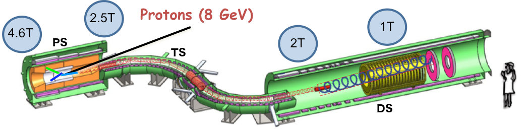
In Fig. 1, the layout of the Mu2e experiment is shown. A large solenoidal system is used to produce and transport a negative muon beam to an aluminum target. A pulsed beam of 8 GeV protons is sent on a tungsten target inside the Production Solenoid (PS) to produce low momentum pions and muons that are then funnelled by the graded field inside the S-shaped Transport Solenoid (TS). Here, the pions decay to muons and a charge selection is performed by means of a middle section collimation system. Finally, a very intense pulsed negative muon beam (sec) enters the Detector Solenoid (DS) and is stopped on an aluminum target. In three years we expect to collect 6 muon stops, sufficient to reach our goal. Decay products are analized by the tracker [5] and calorimeter [6] systems. Cosmic ray muons can produce fake CE candidates when interacting with the detector materials. In order to reduce their contributions the external area of the DS, and a part of the TS, are covered by a Cosmic Ray Veto (CRV) [7] system.
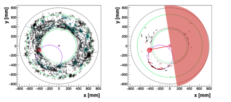
Around 50% of the muon beam is stopped by the target while the rest ends on the beam dump at the end of the cryostat. Muons stopped in the aluminum target are captured in an atomic excited state and promptly cascade to the 1S ground state, with 39% decaying in orbit (DIO) and the remaining 61% captured by the nucleus. Low energy photons, neutrons and protons are emitted in the nuclear capture process. They constitute an irreducible source of accidental activity that is the origin of a large neutron fluence on the detection systems. Together with the flash of particles accompanying the beam, the capture process produces the bulk of the ionising dose observed in the detector system and its electronics. The tracking detector [5], composed of 20000 low mass straw drift tubes, measures the momenta of the charged particles by reconstructing their trajectories with the detected hits. Full simulation shows that a momentum resolution of O(120 keV) is reached, thus allowing separation of the CE line from the falling spectrum of the DIO electrons. The calorimeter plays an important role, complementary to the tracker, by providing particle identification capabilities, a fast online trigger filter and a seed for track reconstruction. In Fig. 2, the large reduction of tracking hits correlated with calorimeter timing is shown. The calorimeter should also be able to maintain functionality in a harsh radiation environment and to work in the presence of 1 T axial magnetic field and in a region evacuated to Torr.
II Calorimeter requirements, technical specifications and calorimeter design
The tasks to be fulfilled by the calorimeter system translate to achieving the following requirements for 105 MeV electrons: (a) a large acceptance; (b) a time resolution better than 0.5 ns; (d) an energy resolution and (d) a position resolution of 1 cm.
II-A Technical choices
In order to satisfy these requirements, we have opted for a high quality crystal calorimeter with Silicon Photomultipliers (SiPMs) readout and with a geometry organised in two annular disks (Fig. 3) to maximise acceptance for spiralling electrons. The crystals should provide a high light yield of at least 40 photo-electrons (p.e.)/MeV. To reconstruct the events with a high pile-up of particles, fast signals are required for the combined choice of crystals and SiPMs, thus reducing the selection of crystals to ones with a decay time () 40 ns. The Front End Electronics (FEE) should provide fast amplified signals to be sampled at 200 Msps (5 ns binning) by the digitisation system. Selected crystals (SiPMs) should also be able to sustain a dose of 450 Gy (200 Gy) and a neutron fluence of of ncm2 while satisfying the calorimeter performance. Moreover, in order to allow operating the detector inside the DS, without interruption for one year, a high redundancy is required on the integrated system. This translates onto having two independent SiPMs, FEE amplifiers and HV regulator chips/crystal as well as having a completely independent digitisation system for the two readout lines. A simulation demonstrated that the typical Mean Time To Failure (MTTF) needed to maintain a fully performing calorimeter along the planned three years of running is of 106 hours/component.
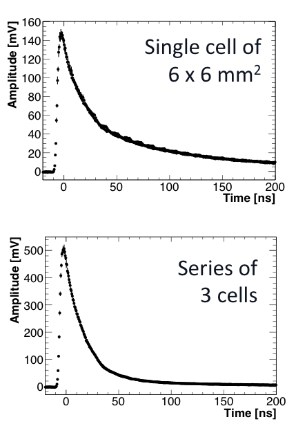
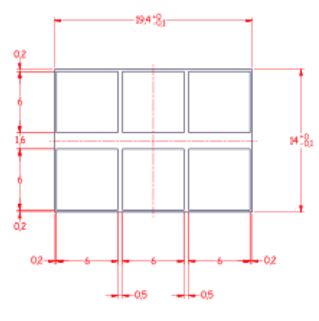
After a long R&D program [8, 9, 10, 11], a final downselect of the scintillating crystal and photosensor has been done. Undoped CsI crystals were chosen as the best compromise between cost, performance and reliability. Indeed these crystals are sufficiently radiation hard for our purposes, have a fast emission time and a large enough light yield. However, the main scintillation component is emitted at a wavelength of 310 nm so that, to well match the SiPM Photon Detection Efficiency (PDE) as a function of wavelength, we have selected the new generation of UV extended SiPMs. In these sensors, the epoxy resin in the front window has been substituted by a silicon resin thus providing PDE from the blue region down to 280 nm. In sect. III.B (Fig. 8), the PDE measured at 310 nm is shown in good agreement with the vendor specifications. Since we operate in vacuum, the coupling between crystals and SiPMs is done without any optical grease (or glue) thus avoiding the related outgassing contribution. This choice decreased the SiPM light collection efficiency of a factor of two. To recover this loss, we opted for a very large area SiPM array. In Fig. 4, the design of the Mu2e custom SiPM configuration is shown, consisting of a 23 array of 66 mm2 SiPMs, i.e. a parallel of 2 series of 3 sensors. This configuration choice has been done to reduce the overall array capacitance and the quenching time of the array while simplifying the FEE design. This is shown in Fig. 5, where the quenching time for the series of 3 cells is compared with the one of a single cell. As expected the SiPM signal of the series configuration is much narrower than that of a single cell.
II-B Calorimeter design
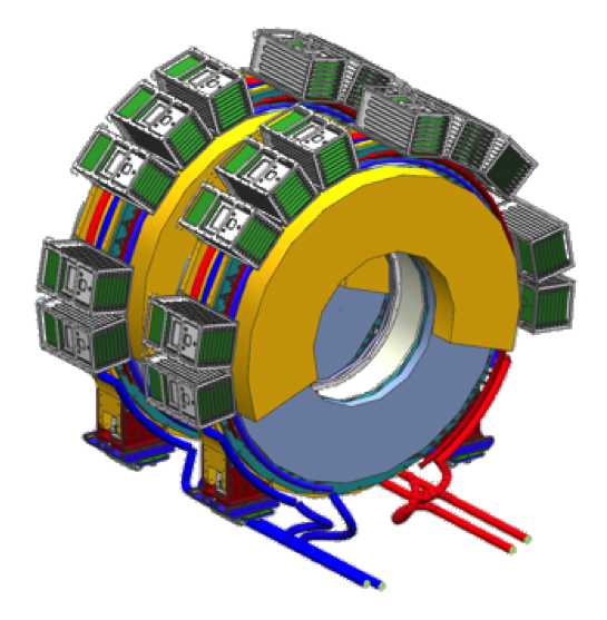
A CAD of the calorimeter system is shown in Fig. 3. The calorimeter consists of two annular disks, each one made of 674 un-doped CsI crystals of parallelepiped shape and dimension of 3.4 3.4 20 cm3. The calorimeter crystal stack has an inner (outer) radius of 37.4 (66.0) cm; the central hole allowing the residual muon beam, the beam flash and most of the DIO electrons to pass through it without interacting. The granularity has been selected for optimising readout and the digital data throughput. The length of the crystals is only 10 X0 but is sufficient to contain the 105 MeV electron showers since the electrons impinge on the calorimeter surface with a 50∘ impact angle. Each crystal is read by two Mu2e custom SiPMs. Each photosensor is amplified and regulated in bias voltage by means of a FEE custom chip. The digitisation system at 200 Msps is located in the nearby crates.
The crystal by crystal equalization is obtained by means of a calibration system, formerly devised for the BaBar calorimeter [12], where a 6.13 MeV photon line is obtained from a short-lived 16O transition. The decay chain comes from the FluorinertTM coolant liquid that is activated by fast neutrons. The activated liquid circulates in aluminium tubes positioned in the front calorimeter plate to uniformly illuminate each crystal face. The source system is accompanied by a laser monitoring system that provides a continuous monitoring capability of the sensor gains and timing offsets, while offering a simple method to monitor variations also on the energy and timing resolutions. Usage of cosmic ray and DIO events is foreseen for a continuous in-situ calibration during running.
A full report of the calorimeter design can be found in [13]. In the following we extract the most relevant information for a consistent explanation while reporting the preliminary measurements done with Module-0.
II-C Test of calorimeter performance
Before completing the engineering design and starting production, we have tested the quality of our design by performing a full simulation of the calorimeter response and a test beam on a small size prototype.
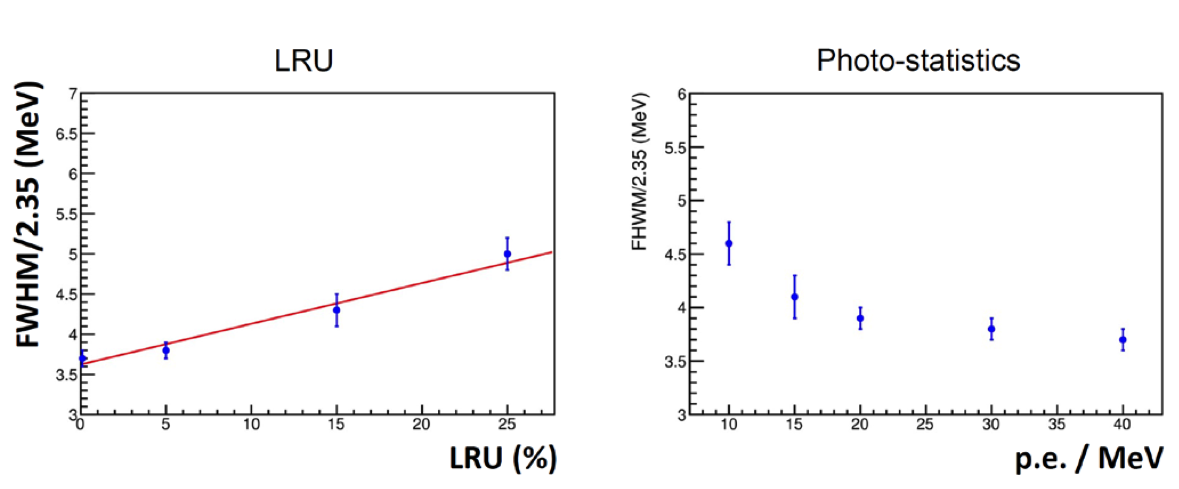
A calorimeter simulation of CE events has been performed with Geant4, in the Mu2e software framework. This simulation includes: (i) the overlap inside the event (pile-up) of the accidental background activity coming from DIO and muon capture events, (ii) a full description of the signal shapes related to the convolution of scintillation, SiPM and FEE response and (iii) a description of the main elements of the mechanical structure. As an example, in Fig. 6, the energy resolution dependence on light yield (LY), expressed as the number of photoelectrons (p.e.)/MeV, and on the longitudinal response uniformity (LRU) are shown. The Mu2e calorimeter design looks robust against variation of the parameters providing resolution better than 5%. However, the optimal working point is observed for LY 20 p.e./MeV for each SiPM and a LRU 5%.
A calorimeter prototype consisting of a matrix of mm2 un-doped CsI crystals wrapped with 150 m Tyvek, each read out by one mm2 SPL TSV Hamamatsu MPPC, has been tested with an electron beam at the Frascati Beam Test Facility (BTF) in April 2015. The final choice of calorimeter wrapping was done after a test of alternatives (Teflon, Tyvek and Aluminum foils) by considering their light yield collection, their radiation hardness and their easiness on the wrapping technique. The best light collection was obtained by means of 8 layers of 20 m Teflon, its difference with 150 m Tyvek (Al) foils was at the level of +10 (25) %. All options were good for radiation resistance. We finally opted for Tyvek for reproducibility in the wrapping method.
The test beam results, described in [10], are consistent with a dedicated Geant-4 simulation and provide:
-
•
a time resolution better than 120 ps for 100 MeV electrons, ranging from about 250 ps at 22 MeV to about 120 ps in the energy range above 50 MeV;
-
•
an energy resolution of for 100 MeV electrons, dominated by shower leakage and beam energy spread.
III Status of preproduction
After freezing the design, in 2016 we have carried out a pre-production of the basic components to control specifications and select vendors for the final production phase. In the following sections, we describe pre-production of crystals, SiPMs and electronics.
III-A Pre-production of crystals
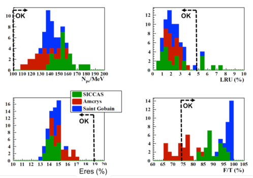
A total of 72 crystals, of final dimension and shape, have been procured from three vendors: St. Gobain (France), SICCAS (China) and Amcrys (Ukraine). All crystals have been exposed to a very accurate Quality Assurance phase. As soon as received at Fermilab, a test of their mechanical precision, both on dimension and shape, has been carried out at the Coordinate Measuring Machine of the SiDET facility. We have then measured (both at Frascati and Caltech) their optical quality by determining, for each crystal, the light yield, the LRU, the energy resolution at 511 keV and the Fast/Total component (i.e., the ratio of the energy seen integrating the signal in 200 ns with respect to the total signal integrated in 3 s). Fig. 7 shows a summary of the crystals’ optical properties. The LY measurement have been carried out with UV extended photomultipliers in order to improve the resolution of the 511 keV peak and to simplify the comparison with the quality control from the producers. A test of the radiation induced noise and of the radiation hardness to dose and neutron fluence has also been carried out. A full report on these measurements can be found in another contribution to these proceedings [14]. At the end of the pre-production phase, we have decided to use both St. Gobain and SICCAS firms for the production crystals, in order to minimise schedule risks.
III-B Pre-production of SiPMs
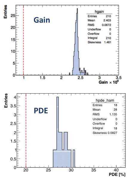
A total of 150 Mu2e SiPMs has been procured from three vendors: Hamamatsu (Japan), SensL (Ireland) and Advansid (Italy). All received SiPMs have been exposed to a very accurate Quality Assurance phase. As soon as received in Pisa, they have been tested in a semi-automated station for their basic properties. These SiPMs have been kept to a constant temperature of 20 ∘C by means of a Peltier cell and a copper line. All measurements were performed for each of the six cells in the array. For each cell, we measured the I-V curve, determined the breakdown voltage, Vbr and derived the operating voltage, Vop, as 3 volts above Vbr. For each SiPM array, the Idark spread at the operating voltage has also been determined. The SiPM gain of each cell was evaluated by means of a photon-counting technique, at the chosen Vop, with a high gain amplifier. Fig. 8.top shows the gain distribution for all pre-production Hamamatsu SiPMs. Finally, the photon detection efficiency (PDE) of each cell was determined by illuminating the sensors with a pulsed LED and extracting the number of events with N and with N 1. The result has been then cross-calibrated with the known PDE of a reference SiPM. The PDE distribution obtained for the Hamamatsu SiPMs is shown in Fig. 8.bottom.
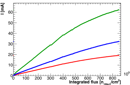
The SiPMs were also tested for their radiation hardness by exposing them both to an ionizing dose and to a neutron fluence. The total irradiation dose (TID) was delivered at the Calliope facility of ENEA Casaccia, Italy. A single sensor was exposed to a high intensity 60Co source integrating a TID of 200 Gy, that is our requirement limit. A small increase in the leakage current has been observed with negligible effect on the SiPM response. The test with neutrons was carried out at the EPOS facility in HZDR, Dresden, Germany. In this facility, a 30 MeV electron beam, of O(100 A) current, interacts with 1 cm thick tungsten target and becomes a good source of photons and neutrons. The target is shielded with lead and borated polyethylene. Above the shielding roof, a clean neutron flux centered at 1 MeV, with negligible photon contamination, is available for testing. One SiPM per vendor has been exposed to a fluence up to 8.5 n(1 MeV)/cm2. A linear increase of the dark current as a function of the fluence is observed, with a different slope between vendors (see Fig. 9.left). In the hottest calorimeter places, we expect to integrate, during the experiment, a fluence of up to 1.21012 n(1 MeV)/cm2 (5 years of running and a simulation safety factor of 3). In the case of the best vendor and after annealing, this irradiation level corresponds to a dark-current of 30 mA, i.e. a power consumption of 4.5 W/SiPM that makes the SiPMs unusable. The solution is to limit the current drawn up to a maximum acceptable value of 2 mA by using two handles: (i) cool down the SiPM at a running temperature of 0 ∘C and (ii) apply a reduction in operating voltages.
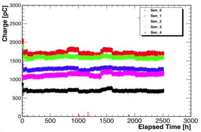
A measurement of the MTTF for the different SiPMs has also been carried out. A group of 5 pieces/vendor has been stressed for 3.5 months by operating them at Vop inside a light tight box kept at a temperature of 50 ∘C. During this stress-test period, the sensors were continuously monitored by: (i) controlling their response to a pulsed LED fired every 2 minutes and (ii) registering the behaviour of the dark current with time. All SiPMs under test were still alive and perfectly working at the end of the stress period. Assuming an acceleration factor of 100 (due to the difference between experiment and stress temperatures) we have estimated an MTTF larger than 6 hours for each vendor. This first determination of MTTF already grants a safe running condition for the first two years of running. A more dedicated measurement will be carried out during the SiPMs production phase.
III-C Preproduction of electronics
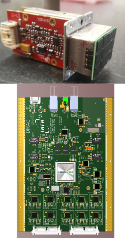
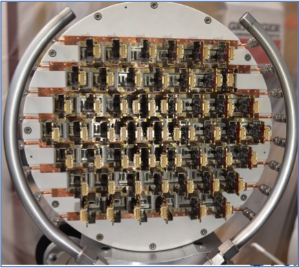
The front-end electronics (FEE) consists of two discrete and independent chips (Amp-HV), for each crystal, directly connected to the back of the SiPM pins. These provide the amplification and shaping stage, a local linear regulation of the bias voltage, monitoring of current and temperature on the sensors and a test pulse. In Fig. 11.top, an example of the left/right FEE chips inserted in the SiPM holder is shown. For equipping the Module-0 (see sub-sec V), a first pre-production of 150 FEE chips has been carried out. A second version will be produced to tune the amplification value and the shaping section, after completing the analysis of the test beam data.
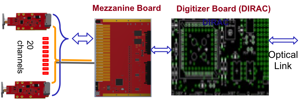
Each disk is subdivided into 34 similar azimuthal sectors of 20 crystals. Groups of 20 Amp-HV chips are controlled by a dedicated mezzanine board (MB), where an ARM controller distributes the LV and the HV reference values, while setting and reading back the locally regulated voltages. Groups of 20 signals are sent differentially to a digitizer module (DIRAC, DIgitizer and ReAdout Controller) where they are sampled (at 200 Msps) and processed before being optically transferred to the T-DAQ system. The Detector Control System (DCS) parameters, read out/set by the MB, are passed via I2C to the DIRAC boards that then communicate them to the Mu2e DCS system through an optical link. In Fig. 11.bottom, a picture of the version-0 of the DIRAC board is shown.
IV Engineering design
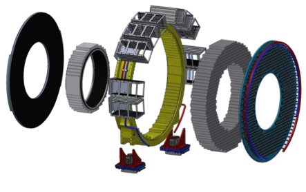
Figure 12 shows an exploded view of a single calorimeter annulus. It consists of an outer monolithic Al cylinder that provides the main support for the crystals and integrates the feet and adjustment mechanism to park the detector on the rails inside the detector solenoid. The inner support is made of a carbon fiber cylinder that maximises , i.e. minimises the passive material. The crystals are then sandwiched between two cover plates. A front plate in carbon fiber intercepts the electrons coming from target. It also integrates the thin wall Al pipes of the source calibration system to flow the FluorinertTM. A back plate, made of PEEK, with apertures in correspondence of each crystal, is used to lodge the FEE and SiPM holders. The back plate houses also the copper pipes where a coolant is flowed to thermalise the photosensors to low temperature and extract the power dissipated by both FEE and sensors. Ten custom-made crates are arranged on top of the outer cylinder and are connected to the cooling circuit to cool the digitizer boards.
A full scale mock-up of the mechanical structure is being built to test the assembly of the crystals, FEE electronics, cooling system and the overall structure robustness. The Al outer ring, the inner Carbon Fiber cylinder, quadrant sections of the front and back plates and one crate have already been manufactured. A whole annulus will be assembled using a mixture of fake iron crystals and a sample of pre-production CsI crystals.
V Design, assembly and test of Module-0
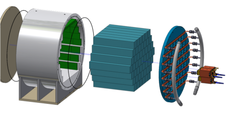
A large size prototype, dubbed Module-0, was built using components of final size and dimensions to resemble a portion of a final disk and to test all final elements for crystals, sensors, mechanics and electronics. Fig. 13 shows an exploded view of the Module-0 CAD drawings to present the various components. This detector is composed by 51 CsI pre-production crystals, each one instrumented with two pre-production Mu2e custom SiPMs. The first version of SiPM copper holders and FEE chips (Fig. 11.top) was used. This allowed to test the gluing procedure of SiPMs on the copper holders, the pre-amplification and HV regulation schemes and the cooling performance. The cooling and FEE support disk was built, as in the final detector, with an insulated support milled to lodge both the copper cooling lines and the SiPM/FEE holders. The only difference with respect to the final version is the insulating material used (Zedex instead of Peek).
The prototype was equipped with two FEE chips/crystal in the central crystal and in the surrounding ring, and with one FEE chip/crystal in all other rings. The readout was organised in five mezzanine boards (16 channels/each), in NIM format, to set and read HV and temperature for all SiPMs. Digitisation was performed with two commercial boards from CAEN, each with 32 channels of 1 GHz digitisers (DRS4).
V-A Test beam results
The Module-0 was exposed to an electron beam with energy between 60 and 120 MeV at the Beam Test Facility (BTF) of Laboratori Nazionali di Frascati of INFN, in the week 8-15 of May 2017. The system integration was really successful. The cooling system was properly working allowing us to keep the sensors’ temperature at (20 1)∘C. We collected few scans in energy and position with beam at normal incidence and some special runs at 50 degrees to simulate the impact angle we will experience in the Mu2e experiment.
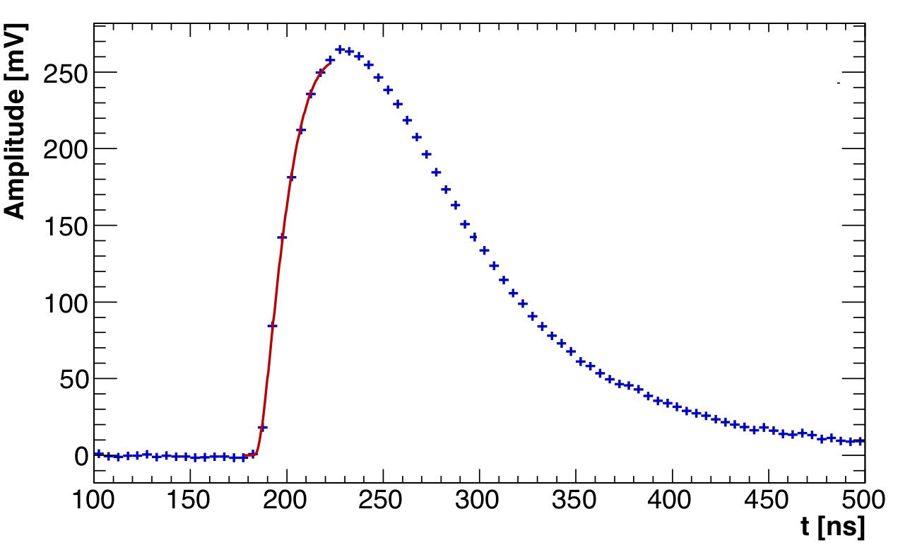
In Fig. 15, the pulse height observed in the central crystal for 100 MeV electrons is shown. The rise-time of the signal is of around 30 ns, while the convoluted decay time of scintillation light, SiPM response and FEE shaping has a of 50 ns, for a total signal width of 350 ns. The charge of each channel is obtained, after subtracting the baseline, with a signal integration time of 250 ns.
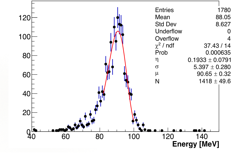
In Fig. 16.a, the energy distribution for 100 MeV electrons at normal incidence is shown. This was obtained summing up the charge of all calorimeter channels with an energy deposition larger than 5 , that represents the noise level determined with a Gaussian fit to the response observed without beam. Channel by channel equalization was done reconstructing the energy deposited by cosmic ray events selected with external scintillation counters. This calibration is in good agreement with an independent determination based on samples of 100 MeV electrons sent in the center of each crystal in the two innermost rings. The energy plot has been fit with a log-normal function as shown by the red curve overimposed. An energy resolution better than 6% is obtained, thus improving the result found with the small size prototype and satisfying the calorimeter requirement.
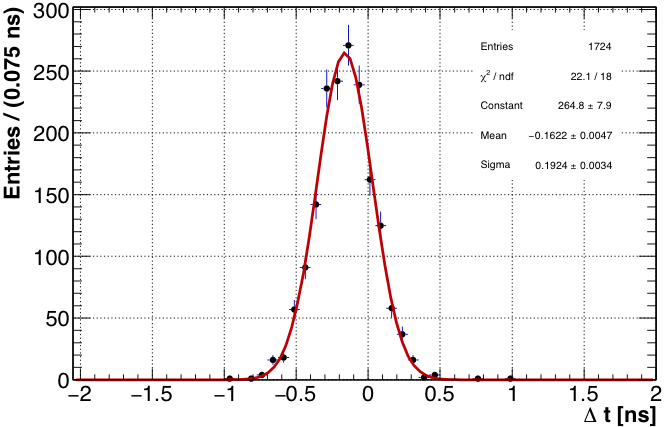
The timing resolution of the calorimeter was also investigated. The rise time of each signal shape was fit to determine the crossing time, as shown in Fig.15. The distribution of the timing difference between two SiPMs of the central crystal is shown in Fig. 16.b for 100 MeV electrons. A timing resolution of 96 ps is estimated when considering the semi-difference of the two times. This estimate takes into account the resolution related to photoelectron statistics and readout electronics but it does not consider the jitter due to shower fluctuation or clock synchronisation. Further measurements are planned to clarify these contributions.
VI Conclusions and perspectives
The Mu2e calorimeter is a state of the art crystal calorimeter with excellent energy (%) and timing ( 500 ps) resolutions, for 100 MeV electrons, and a good pileup discrimination capability. The latter one is obtained thanks to the chosen crystals and sensors assisted by a fast analog electronics and a digitisation at 200 Msps. There are many demanding requests to be satisfied by this detector, such as to keep the required performance in presence of 1 T axial magnetic field, in an evacuated region and in a radiation harsh environment. The CsI crystals will withstand the expected dose and fluence with a small light yield loss. The Mu2e SiPMs will work under neutron irradiation when cooled to 0 ∘C, thus asking for a good engineering design of the calorimeter mechanics and of its cooling system. Pre-production of crystals and SiPMs has been successfully carried out in 2016 demonstrating that the required technical specifications can be met. Final vendors have been selected and the production will start at the end of 2017. Pre-production for the electronics is also under way. The calorimeter Module-0 has been built in April 2017 to exercise the final selected components and the engineering of mechanical and electronic systems. A full size mock-up of the calorimeter disk is underway to test the assembly procedure. The schedule is to start assembly the first disk in winter 2018 and complete the calorimeter construction in 2020.
Acknowledgment
We are grateful for the vital contributions of the Fermilab staff and the technical staff of the participating institutions. This work was supported by the US Department of Energy; the Italian Istituto Nazionale di Fisica Nucleare; the Science and Technology Facilities Council, UK; the Ministry of Education and Science of the Russian Federation; the US National Science Foundation; the Thousand Talents Plan of China; the Helmholtz Association of Germany; and the EU Horizon 2020 Research and Innovation Program under the Marie Sklodowska-Curie Grant Agreement No.690385. Fermilab is operated by Fermi Research Alliance, LLC under Contract No. De-AC02-07CH11359 with the US Department of Energy, Office of Science, Office of High Energy Physics. The United States Government retains and the publisher, by accepting the article for publication, acknowledges that the United States Government retains a non-exclusive, paid-up, irrevocable, world-wide license to publish or reproduce the published form of this manuscript, or allow others to do so, for United States Government purposes.
References
- [1] Mu2e Collaboration, FERMILAB-TM-2594, ArXiv:1501.05241 (2015).
- [2] S.M.Bilenky et al., Phys. Lett. B67, p 309 (1977)
- [3] F.Grancagnolo et al., Nucl.Phys.Proc.Supp. 248-250, p 1-146 (2014).
- [4] The SINDRUM II Collaboration, Eur.Phys.J. C47, p 337-346 (2006)
- [5] MyeongJae Lee (Mu2e collaboration), Nuclear and Particle Physics Proceedings, Vol 273-275, p 2530-2532 (2016).
- [6] N.Atanov et al., Nucl. Instr. and Meth. A 824 p 695-698 (2016).
- [7] A. Artikov et al. (Mu2e CRV group), ArXiv:1511.00374 (2015).
- [8] N. Atanov et al., Nucl. Instr. and Meth. A 812 p 104 (2016).
- [9] N. Atanov et al., Nucl. Instr. and Meth. A 824 p 684 (2016).
- [10] D.Hitlin et al., Nucl. Instr. and Meth. A 824 p 119 (2016).
- [11] O. Atanova et al., JINST 12 (2017) P05007.
- [12] B. Aubert et al., Nucl. Instr. and Meth. A 479 p 1 (2002).
- [13] N, Atanov et al. (Mu2e Calorimeter), Mu2e Docdb N. 8429 , (2016).
- [14] R.Y. Zhu (Mu2e Calorimeter), in these proceedings.