Strain Mapping In Single-Layer 2D Crystals Via Raman Activity
Abstract
By performing density functional theory-based ab-initio calculations, Raman active phonon modes of novel single-layer two-dimensional (2D) materials and the effect of in-plane biaxial strain on the peak frequencies and corresponding activities of the Raman active modes are calculated. Our findings confirm the Raman spectrum of the unstrained 2D crystals and provide expected variations in the Raman active modes of the crystals under in-plane biaxial strain. The results are summarized as follows; (i) frequencies of the phonon modes soften (harden) under applied tensile (compressive) strains, (ii) the response of the Raman activities to applied strain for the in-plane and out-of-plane vibrational modes have opposite trends, thus, the built-in strains in the materials can be monitored by tracking the relative activities of those modes, (iii) in particular, the A-peak in single-layer Si and Ge disappear under a critical tensile strain, (iv) especially in mono and diatomic single-layers, the shift of the peak frequencies is stronger indication of the strain rather than the change in Raman activities, (v) Raman active modes of single-layer ReX2 (X=S, Se) are almost irresponsive to the applied strain. Strain-induced modifications in the Raman spectrum of 2D materials in terms of the peak positions and the relative Raman activities of the modes could be a convenient tool for characterization.
pacs:
31.15.A,36.20.Ng, 63.22.Np, 68.35.GyI Introduction
The successful synthesis of graphene,Novoselov2 opened a new, famous field of research, 2D single-layer materials. 2D materials have attracted great attention due to their extraordinary electronic, optical, and mechanical properties that suit technological applications such as energy conversion, flexible electronics and information technologies.Wang1 ; Bhimanapati ; Akinwande ; Mak Following graphene, new 2D single-layer structures such as transition-metal dichalcogenides (TMDs)Gordon ; Coleman ; Ross ; Sahin2 ; Tongay ; Horzum ; Chen3 ; myk mono-elemental 2D materials such as silicene,Cahangirov ; Kara germanene,Cahangirov and group III-V binary compounds (-BN, -AlN)Sahin3 ; Wang2 ; Kim ; Tsipas ; Bacaksiz were successfully synthesized. In addition to those in-plane isotropic single-layers, 2D materials with in-plane anisotropy such as ReS2Tongay ; Chenet ; Hart ; myk1 , ReSe2Yang1 ; Yang2 , and black phosphorus (bp) were also widely studiedbp1 ; bp2 ; bp3 . The improved production methods, such as chemical vapor deposition and mechanical exfoliation, enable the synthesis of thinner and cleaner structures.
One of the most common technique for the characterization of a material is Raman spectroscopyraman which crops information about the nature of the material medium entities by monitoring the characteristic vibrational energy levels of the structure. It also provides non-destructive analysis and requires minimum sample preparation. In addition, Raman measurements are also able to provide information about the substrate-free layer-number identification of layered materials,ferrari ; qiao ; xzhang the strength of the interlayer coupling in layered materials,phtan and interface coupling in van der Waals heterostructures.jbwu ; jbwu2 Moreover, relative intensities of the Raman peaks lead to the determination of different-phase distributions in a material.colom ; gouadec ; havel ; xzhang2
Strain can alter electronic and vibrational properties of materials.guinea ; khe Raman peak positions and intensities strongly depend on the presence of strainzhni ; huang since it modifies the crystal phonons, with stretching usually resulting in mode softening, and the opposite for compressing. The rate of change is summarized in the Gruneissen parameters which determines the thermomechanical properties. Moreover, strain enhances the Raman spectrum of 2D materials in terms of the Raman intensities. Although, Raman spectroscopy has been widely studied in literature,ferrari2 ; berkdemir ; chenet ; frostig detailed theoretical investigation of the strain effects on Raman peaks for 2D materials is still limited. Here, we theoretically investigate the strain-dependent vibrational properties of several 2D single-layer materials in terms of the peak frequencies and corresponding Raman activities.
The paper is organized as follows: Details of the computational methodology is given in Sec. II. The theory of Raman activity calculations is briefly explained in Sec. III. The evolution of peak frequencies and corresponding Raman activities under in-plane biaxial strain are discussed In Secs. III.1, III.2, and III.3 for monoatomic, diatomic, and isotropic single-layer TMDs, respectively. And those for in-plane anisotropic single-layers of ReX2 and bp are presented in Secs. III.4.1 and III.4.2 Finally, we conclude in Sec. IV.
II Computational Methodology
For structural optimization and vibrational properties of considered materials, first principle calculations were performed in the framework of density functional theory (DFT) as implemented in the Vienna ab-initio Simulation Package (VASP).vasp1 ; vasp2 The Perdew-Burke-Ernzerhof (PBE)perdew form of generalized gradient approximation (GGA) was adopted to describe electron exchange and correlation. The van der Waals (vdW) correction was included by using the DFT-D2 method of Grimme.grimme The charge transfer between individual atoms was determined by the Bader technique.bader
The kinetic energy cut-off for plane-wave expansion was set to 800 eV and the energy was minimized until its variation in the following steps became 10-8 eV. The Gaussian smearing method was employed for the total energy calculations and the width of the smearing was chosen as 0.05 eV. Total Hellmann-Feynman forces in the until was reduced to 10-7 eV/Å for the structural optimization. 18181 centered k-point samplings were used or the primitive unit cells. For 22 reconstructed supercell of ReX2 structures, k-point sampling is reduced to 12121 mesh. To avoid interaction between the adjacent layers, our calculations were implemented with a vacuum space of 25 Å.
The vibrational properties of all single-layer crystals were calculated in terms of the off-resonant Raman activities of phonon modes at the point. For this purpose, first the vibrational phonon modes at the point were calculated using finite-displacement method as implemented in VASP. Each atom in the primitive unit cell was initially distorted 0.01 Å and the corresponding dynamical matrix was constructed. Then, the vibrational modes were determined by a direct diagonalization of the dynamical matrix. The -point set was increased step by step up to 24241 until the convergence for the frequencies of acoustical modes was reached (0.0 cm-1 for each acoustical mode). Once the accurate phonon mode frequencies were obtained, the change of macroscopic dielectric tensor was calculated with respect to each vibrational mode to get the corresponding Raman activities.
In order to investigate the response of the peak frequencies to the applied biaxial strain for Raman active modes, the rate of change of the peak frequency and the corresponding mode Gruneissen parameter were calculated. The mode Gruneissen parameter at any wave vector, , can be calculated by the formula;
| (1) |
where is the relaxed (unstrained) lattice constant, (q) is the unstrained phonon frequency at wave vector , (q) and (q) are the phonon frequencies under tensile and compressive biaxial strain, respectively, and is the difference in the lattice constant when the system is under biaxial strain. In the present study, the phonon frequencies are calculated in the =0 limit, at the .
| Point | of | |||||||||||
|---|---|---|---|---|---|---|---|---|---|---|---|---|
| Structure | Group | Raman Active | Cx | Cy | ||||||||
| (Å) | (Å) | Modes | (eV) | (N/m) | (N/m) | |||||||
| Graphene | PL | 2.47 | 2.47 | D3h | 2 | 23.31 | (2410-6)Gmitra | 330 | 330 | 0.19 | 0.19 | |
| Silicene | LB | 3.85 | 3.85 | D3d | 3 | 8.01 | 0.001-0.01Tabert | 54 | 54 | 0.41 | 0.41 | |
| Germanene | LB | 4.01 | 4.01 | D3d | 3 | 9.04 | 0.02-0.1liu-1 ; liu-2 | 38 | 38 | 0.42 | 0.42 | |
| h-BN | PL | 2.51 | 2.51 | D3h | 2 | 1.5 | 2-4BN | 4.68(d) | 273 | 273 | 0.22 | 0.22 |
| h-AlN | PL | 3.13 | 3.13 | D3h | 2 | 1.46 | 3.61(i) | 112 | 112 | 0.46 | 0.46 | |
| h-GaN | PL | 3.27 | 3.27 | D3h | 2 | 1.71 | 2.37(i) | 109 | 109 | 0.48 | 0.48 | |
| MoS2 | 1H | 3.19 | 3.19 | D3h | 5 | 4.46 | 4.2-7.6Huser | 1.56(d) | 122 | 122 | 0.26 | 0.26 |
| MoSe2 | 1H | 3.32 | 3.32 | D3h | 5 | 5.02 | 4.74Ramasubramaniam | 1.33(d) | 109 | 109 | 0.25 | 0.25 |
| WS2 | 1H | 3.18 | 3.18 | D3h | 5 | 4.12 | 4.13Ramasubramaniam | 1.53(d) | 122 | 122 | 0.21 | 0.21 |
| WSe2 | 1H | 3.33 | 3.33 | D3h | 5 | 4.67 | 4.63Ramasubramaniam | 1.19(d) | 99 | 99 | 0.20 | 0.20 |
| ReS2 | 1T | 6.46 | 6.38 | C1h | 18 | 4.18* | 1.34(d) | 166 | 159 | 0.19 | 0.19 | |
| ReSe2 | 1T | 6.71 | 6.60 | C1h | 18 | 4.71* | 1.27(d) | 138 | 138 | 0.18 | 0.18 | |
| bp | P | 4.57 | 3.31 | D2h | 6 | 4.32* | 0.88(d) | 91 | 29 | 0.65 | 0.21 |
III Strain-dependent raman activity
Basically in the Raman experiment, the sample is exposed to light and instantly scattered photons are collected. The dispersion of the collected photons with respect to shift in frequency gives the Raman spectrum. In the Raman theory, inelastically scattered photon originates from the oscillating dipoles of the crystal correspond to the Raman active vibrational modes of the crystal.
The treatment of Raman intensities is based on Placzek’s classical theory of polarizability. According to the classical Placzek approximation, the activity of a Raman active phonon mode is proportional to where and stand for the polarization vectors of scattered radiation and incident light, respectively. is a 33 second rank tensor called “Raman tensor” whose elements are the derivatives of polarizability of the material with respect to vibrational normal modes,
| (2) |
where the is the normal mode describing the whole motion of individual atoms participating to the vibrational mode and is the polarizability tensor of the material. The term is called the Raman activity which is calculated from the change of polarizability. For a backscattering experimental geometry, if orientational averaging is considered, the Raman activity is represented in terms of Raman invariants given by,
| (3) | ||||
| (4) |
where and represent the isotropic and anisotropic parts of the derivative of polarizability tensor, respectively. The represents the derivative of polarizability with respect to a normal mode. In the representation of the activity in terms of the variables, the activity is invariant under the orientation of sample. Finally, using the forms of isotropic and anisotropic polarizability derivative tensors, the Raman activity, RA, can be written as;
| (5) |
In fact, every Raman active phonon mode has a finite scattering intensity which is measured in experiments. The term Raman activity, RA, is directly related to the intensity through the following formula;
| (6) |
where I0 is the intensity of incoming light, is its wavelength, and RA is the Raman activity. In the rest of the present study, Raman activities are discussed instead of intensities since the Raman activity is independent of the wavelength and the intensity of incoming light and it is given in terms of Raman invariants (see Eq. 5).
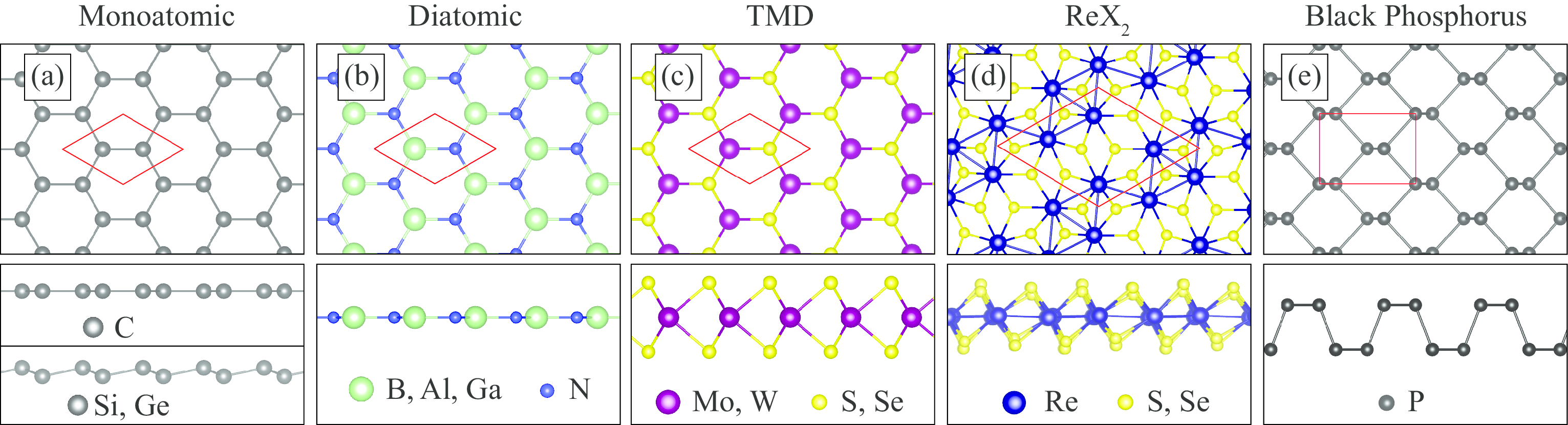
III.1 Mono-Atomic Single-Layer Crystals
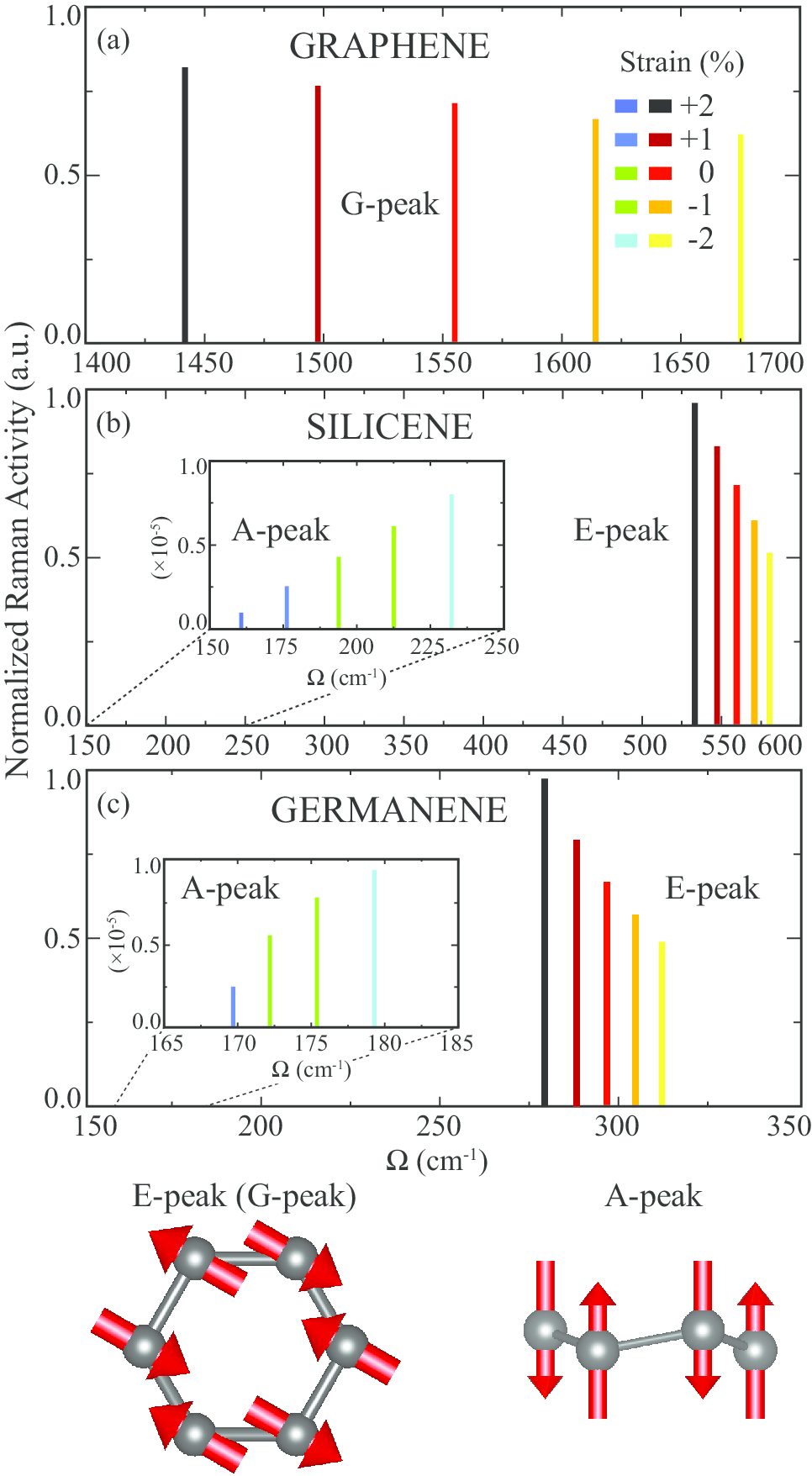
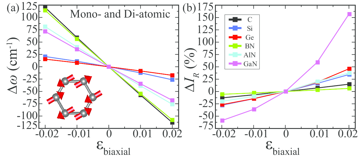
Monoatomic single-layers of graphene, silicene, and germanene have hexagonal crystal structures. Due to sp2 hybridization of C atoms in graphene, its structure is planar and belongs to space group symmetry. On the other hand, sp3 hybridization in silicene and germanene results in a buckled geometry (see Fig. 1(a)). The structure of the two buckled single-layers belong to space group. Graphene, silicene, and germanene are known to exhibit tiny electronic band gap of 2410-3Gmitra , 1.55-7.90 Tabert and 24-93 meVliu-1 ; liu-2 , respectively.
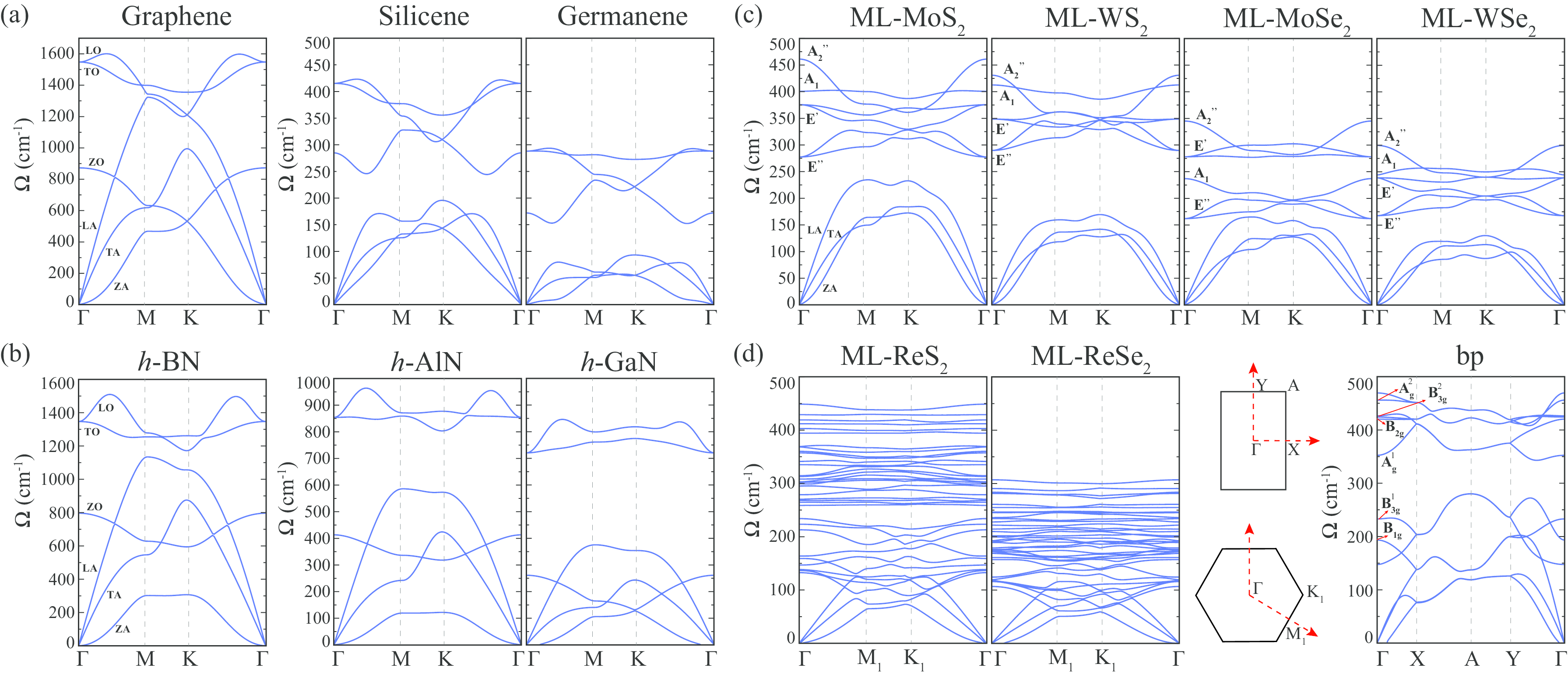
Graphene, silicene, and germanene exhibit 6 phonon branches that consist of 3 acoustical and 3 optical branches (see Fig. 2(a)). One of the optical phonon modes represents out-of-plane vibrational motion of the atoms and named as A-peak phonon mode. The other two optical modes have in-plane vibrational characteristic and known as the G-peak in graphene and E-peak in silicene and germanene. G- and E-peak are doubly degenerate at the due to in-plane isotropy of the crystals.
In the case of graphene, the frequency of A-peak is 872.8 cm-1 and it is Raman inactive due to the planar crystal structure. On the other hand, G-peak is a characteristic Raman active mode in graphene and its frequency is 1555.0 cm-1. When an in-plane biaxial strain is applied to the crystal, a significant phonon softening (hardening) occurs under tensile (compressive) strain cases which is expected due to positive mode Gruneissen parameter (see Table 2). As shown in Fig. 3(a), the frequency of G-peak softens to 1441.8 cm-1 at 2% of tensile strain while it hardens to 1675.1 cm-1 at 2% of compressive strain. The variation of Raman activity of G-peak is also shown in Fig. 3(a). It is seen that as the structure is biaxially stretched, the dipole between oppositely vibrating atoms gets larger, the polarizability increases, and hence the Raman activity increases. Contrarily, when the structure is compressed, the length of the dipole gets smaller and the Raman activity decreases.
The frequency of A-peak is 193.8 cm-1 for silicene and due to the buckled structure A-peak is found to be Raman active. The E-peak frequency is found at 559.6 cm-1 and is known to be another Raman active mode in silicene. Experimentally, E-peak is much more prominent than the A-peak due to its much higher Raman activity. The Raman activity of E-peak is 105 times of that of the A-peak. As shown in Fig. 3(b), when biaxial strain is applied, both peaks soften (harden) under tensile (compressive) strain cases. However, the response of Raman activities of A- and E-peak is opposite. As the structure is stretched, the length of dipole in A-peak gets smaller while it gets larger in E-peak. Thus, the polarizability hence the Raman activity of A-peak decreases while the it increases for E-peak. The situation is reversed in the compressive strain case as shown in Fig. 3(b). The important point is that the Raman activity of A-peak may disappear under high tensile strain values (2%) as the buckling of the structure decreases.
For the germanene, the peak position of A-peak is at 172.2 cm-1. Since germanene is a softer material than silicene, the peak frequency of A-peak is smaller. As in the case of silicene, A-peak is Raman active for germanene due to the sp3 hybridization of Ge atoms. The frequency of E-peak is 296.8 cm-1 which is also much smaller than that of in silicene. Both peaks display the same behavior for peak frequencies and corresponding Raman activities as in the case of silicene. As shown in Fig. 3(c), the E-peak displays a phonon softening to 279.4 cm-1 at 2% of tensile strain while it displays a phonon hardening to 312.2 cm-1 at 2% of compressive strain. In addition, the Raman activity of A-peak decreases and disappears at 2% of tensile strain.
Each monoatomic single-layer displays different responses to applied strain. The difference in the slope of the curves in Fig. 5(a) occurs due to different mode Gruneissen parameter() of G- and E-peak in each material. The values are given in Table 2 and graphene has the largest value which is a result of strong C-C bonds in the crystal. As shown in Fig. 5(b), the amount of change of Raman activities are also different for each single-layer crystal. Stiff materials, with strong interatomic bonds, charges are uniformly distributed between the atoms and they are not localized in any region even at relatively high strains. Therefore, the change of dielectric constant hence the change of Raman activity is linear. However, in the case of silicene and germanene the charge is localized between the atoms and thus, as the strain is increased the Raman activity displays a nonlinear change (see Fig. 5(b)).
III.2 Diatomic Single-Layer Crystals
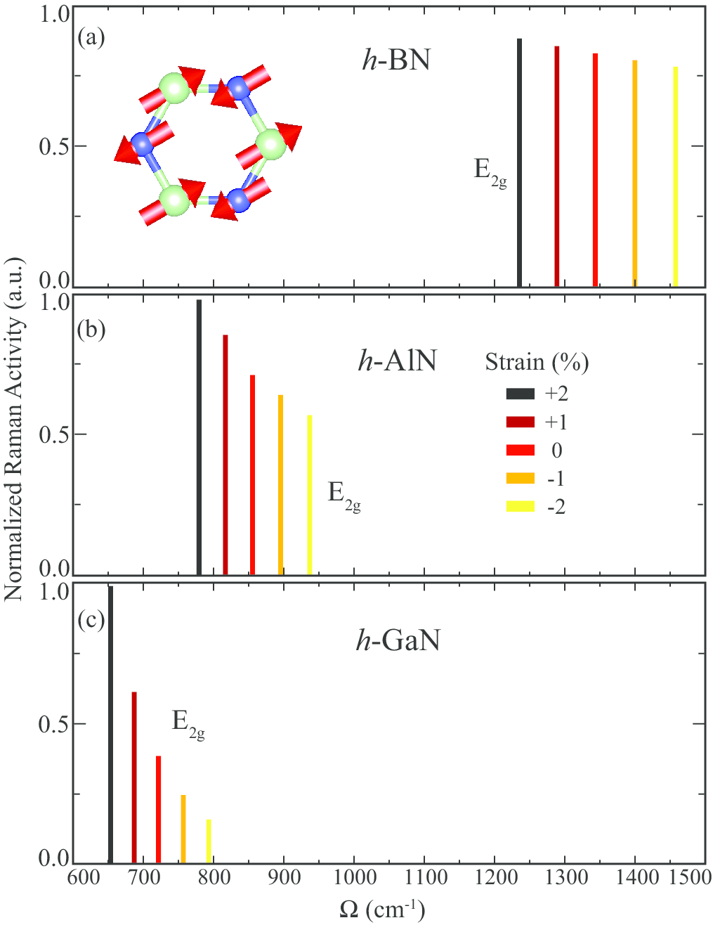
Similar to the crystal structure of graphene, diatomic single-layers of group-III Nitrides (h-BN, h-AlN, and h-GaN) have planar, one-atom-thick structure as shown in Fig. 1(b). The crystal structures belong to space group of P63/mmc. Single-layers of the group-III Nitrides exhibit 6 phonon branches (see Fig. 2(b)). In addition to the A-peak, the doubly degenerate in-plane phonon mode, E2g, are the optical phonon modes of the single-layers. The A-peak is Raman inactive mode for the group-III Nitrides while E2g is the prominent peak.
The frequency of A-peak is 800.9 cm-1 for h-BN while the frequency of E2g is found at 1343.4 cm-1. Due to the occupied in-plane orbitals in the crystal, the frequency of E2g is much greater than that of A-peak. Under biaxial strain, the E2g peak reveals a softening to 1235.5 cm-1 at 2% stretching and displays a hardening to 1457.7 cm-1 at 2% compression. The Raman activity of the E2g peak increases with increasing tensile strain while it decreases with increasing of the compressive strain as shown in Fig. 4(a). As in the case of graphene, the change of Raman activity is also linear for h-BN due to the strong B-N bonds which preserves the charge distribution even at high strains. The response of Raman inactive A-peak to the applied strain is not discussed.
In the case of h-AlN, the frequency of the A-peak softens to 412.5 cm-1 since the stiffness is smaller than that of h-BN. The frequency of E2g is 855.5 cm-1 which is also smaller than that of the h-BN due to the same reason. When the single-layer h-AlN is biaxially stretched, the peak position of E2g softens to 779.4 cm-1 while it hardens to 936.9 cm-1. In addition, the Raman activity displays the same trend as in the case of h-BN but the amount of change is different as shown in Fig. 5(b). The atomic bond length is much larger in h-AlN than that of h-BN thus, increasing strain causes nonlinear change in the Raman activity of h-AlN because of the localized charge densities in the crystal.
The lowest frequencies of both A-peak and the E2g mode are found for single-layer h-GaN since it is the most flexible material through all considered group-III Nitrides. The peak positions of the two modes are 263.6 and 721.6 cm-1 for A-peak and E2g, respectively. The highest rate of change of peak frequency with respect to the unstrained frequency is found for h-GaN as given in Table 2 by the mode Gruneissen parameter.
As shown in Fig. 5(b), the response of Raman activity of each material differs as the applied strain increases. As mentioned in the theory part, the Raman activity is a function of which depends on static dielectric constant, , and the is a function of square of charges on the atoms. Graphene and h-BN display linear response even at 2% strain (see Fig. 5(b)) due to the strong C-C and B-N bonds which preserve charge distribution in the crystal. As the in-plane stiffness decreases, the conservation of charge distribution is not possible with increasing strain value. Thus, silicene and germanene exhibit nonlinear response out of the strain range 1%. Moreover, special to the case of h-GaN, the charges are initially localized on N atoms which indicates relatively weak Ga-N bonding in the crystal. Therefore, even at small strains, the Raman activity of h-GaN displays nonlinear responses.
| (cm-1) | (%) | |||
| Graphene | 1555.0 | 3.75 | 1.87 | 1.85gru2 |
| Silicene | 559.6 | 2.10 | 1.05 | |
| Germanene | 296.8 | 2.78 | 1.39 | |
| h-BN | 1343.4 | 4.13 | 2.07 | 1.70gru3 |
| h-AlN | 855.5 | 4.60 | 2.30 | |
| h-GaN | 721.6 | 4.84 | 2.42 |
| E | E | A1 | ||||||||||
|---|---|---|---|---|---|---|---|---|---|---|---|---|
| (cm-1) | (%) | (cm-1) | (%) | (cm-1) | (%) | |||||||
| MoS2 | 277.8 | 1.04 | 0.52 | 375.8 | 1.36 | 0.68 | 401.0 | 0.46 | 0.23 | |||
| MoSe2 | 162.2 | 0.77 | 0.39 | 278.3 | 1.06 | 0.53 | 237.3 | 0.42 | 0.21 | |||
| WS2 | 289.5 | 0.98 | 0.49 | 348.2 | 1.27 | 0.64 | 412.4 | 0.51 | 0.25 | |||
| WSe2 | 167.9 | 0.77 | 0.39 | 239.0 | 1.08 | 0.54 | 244.4 | 0.44 | 0.22 |
III.3 TMDs Single-Layer Crystals
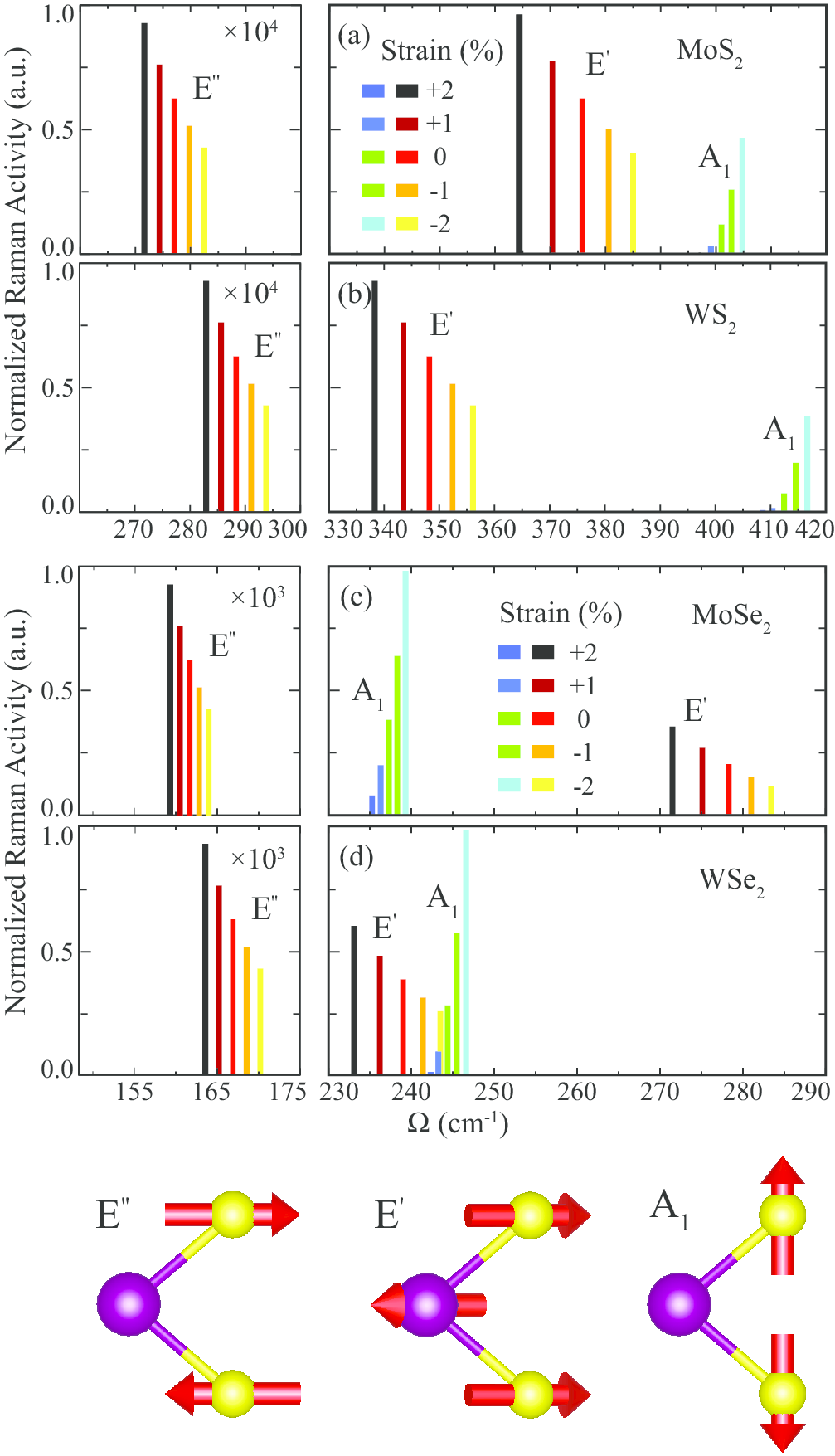
The single-layers of TMDs has a hexagonally packed crystal structure in which the sub-layer of metal (M) atom is sandwiched between two sub-layers of chalcogen (X) atoms (see Fig. 1(d)). Most of the single-layer TMDs crystallize in either 1H or 1T phases. Here, we consider single-layers of Mo- and W-dichalcogenides which have 1H crystal structure. Single-layer crystals of the TMDs exhibit space group symmetry. MX2 (M=Mo or W, X=S or Se) crystals exhibit 9 phonon branches 6 of which are optical phonon branches (see Fig. 2(c)). The group theory analysis indicate that due to the symmetry group there are 5 Raman active modes. The in-plane optical phonon modes are known as the E and E which are both doubly degenerate and Raman active. Additionally, an out-of-plane optical mode, A1, is Raman active (see Fig. 6). Another out-of-plane optical mode, A, is the only Raman inactive mode for the single-layer TMDs.
The E phonon mode is the lowest frequency optical mode which reveals only the vibration of the chalcogen atoms in opposite directions. The frequencies of E are 277.8, 162.5, 289.5, and 167.9 cm-1 for MoS2, MoSe2, WS2, and WSe2, respectively. Since the mass of Se atom is much larger than that of S atom, phonon modes soften in MSe2 crystals. The Raman activity of E mode is much smaller than those of E and A1 modes in each single-layer. In MS2 crystals its Raman activity is in the order of 10-4 while in MSe2 structures the activity is in the order of 10-3. Thus, it is not a prominent Raman peak in the experiments.
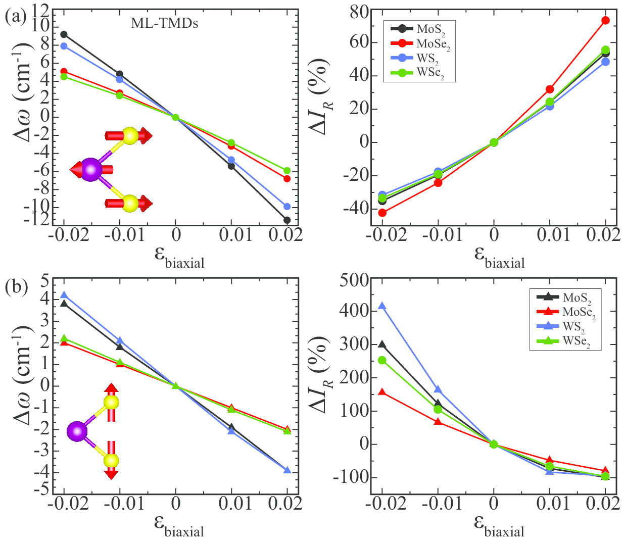
The effect of uniaxial strain on the vibrational spectrum of single-layer MoS2 was investigated by Doratoj et al. and due to the in-plane symmetry breaking in the crystal, the phonon-splitting was showed for the in-plane E mode which is a direct observation of induced strain in the structuredoratoj . In the present study, we try to show to detection of strain under the biaxial case. When the crystals are biaxially stretched, E displays phonon softening and demonstrates a phonon hardening under compressive strains as shown in Fig. 6. The corresponding mode Gruneissen parameters are given in Table 3. Since the Raman activity of E is very small, it is still not prominent even at high tensile strains. Because of the insignificant changes in the Raman activity of E, other two prominent Raman peaks are discussed which may determine the strain in single-layer TMDs.
The E mode demonstrates the vibration of the transition metal atom in opposite direction to the chalcogen atoms. The frequencies of E are 375.8, 278.3, 348.2, and 239.0 cm-1 for MoS2, MoSe2, WS2, and WSe2, respectively. The Raman activity of E indicates that it is a prominent peak clearly observed in experimentsDong . The response of the frequency of E peak to the biaxial strain is discussed through the calculated mode Gruneissen parameter for each single-layer. As given in Table 3, values are 0.68 (0.65)gru1 , 0.53, 0.64, and 0.54 for MoS2, MoSe2, WS2, and WSe2, respectively. The Raman activity of E peak demonstrates a similar response to the biaxial strain with that of in monoatomic and diatomic cases. Due to opposite responses of E and A1 peaks, discussion of their relative Raman activities is more meaningful.
As mentioned above, the A1 phonon mode is the only Raman active out-of-plane optical mode. In all the single-layer TMDs the frequency of A1 mode is higher than that of E except for MoSe2. The frequencies of A1 are 401.0, 237.3, 412.4, and 244.4 cm-1 for single-layer MoS2, MoSe2, WS2, and WSe2, respectively. The higher frequencies in MS2 crystals are due to smaller vertical distance of S-S atoms. In the unstrained single-layer TMDs, the Raman activity of A1 peak is smaller than that of E except for MoSe2. In vdW layered materials, increasing number of layers strongly affects the activity of A1 peak due to additional interlayer interaction. As given in Table 3, values for the A1 peak are smaller than the values for E which means frequency of A1 is less affected by the in-plane strain. This is meaningful since A1 represents the out-of-plane vibration of the atoms. The values for A1 are 0.23 (0.21gru1 ), 0.21, 0.25, and 0.22, respectively. In contrast to response of Raman activity of E to applied strain, the activity of A1 increases when the structure is compressed which is a result of increasing dipole length between vibrating chalcogen atoms when structure is compressed in the in-plane directions.
Although, the Raman activity of both prominent peaks changes under biaxial strain, it is meaningful to discuss their relative ratios to identify the strain in the crystal. The ratios, , in the unstrained structures are 5.35, 0.53, 8.32, and 1.37 for MoS2, MoSe2, WS2, and WSe2, respectively. Since A1 and E demonstrate opposite responses to the biaxial strain, the ratio gets much higher when the structure in stretched. This is an important point for the identification of biaxial strain on the crystal. For the maximum compression (-2%) the ratios are, 0.87, 0.12, 1.11, and 0.26, respectively. Contrary to compressive strain, the values are enhanced under tensile strain case which is a strong indication of the stretched crystal. In the case of MS2 crystals, increases to 574 and 204 for MoS2 and WS2, respectively. High values of the activity ratio can be clearly observed in a Raman experiment in which the samples are under tensile biaxial strain.
III.4 Anisotropic Single-Layer Crystals
III.4.1 Rhenium Dichalcogenides (ReS2 and ReSe2) Single-Layer Crystals
Besides the perfect hexagonal lattice, there are also in-plane anisotropic single-layer crystals such as ReS2, ReSe2 and bp. As shown in Fig. 1(e), single-layers of ReS2 and ReSe2 have distorted 1T (1T′) crystal structure, which belongs to space group of P.tongay Unit cell of 1T′ phase consists of 8 chalcogen atoms coordinated around diamond-like Re4 cluster which is formed by the strong interaction between Re atoms. The angle between the in-plane unit cell vectors is 61.1∘ due to distortion in the crystal structure.
For single-layer ReX2 there are 36 phonon modes as shown in Fig. 2(d). Due to the distorted and anisotropic crystal structure, all of the Raman active phonon modes are non-degenerate. The 18 of the 36 phonon modes for both crystals are known to be Raman active from the group theoryFeng .
The 18 Raman active phonon modes of single-layer ReS2 are classified as Ag-like (representing out-of-plane motion of atoms), Eg-like (representing in-plane motion of atoms), and the coupled vibrations of the atoms in both directions. There are 4 Ag-like modes 2 of which contain the motion of Re atoms while the other 2 contain motion of S atoms. The modes with frequencies of 132.6 and 139.9 cm-1 represent the Ag-like modes of Re atoms while the modes at 429.0 and 402.7 cm-1 represent that of S atoms. The Raman activities of Ag-like modes of Re are smaller than those for the modes of S atoms which is because of the smaller dipole length between Re atoms. The frequencies and the Raman activities of Ag-like modes of both atoms demonstrate similar behavior under applied strain as in other TMDs discussed in Sec. III.3. However, the change of activity of Ag-like modes of Re is much smaller than that of S atoms because at the strength of applied strain the length of Re-Re dipole is still small due to their strong interaction.
The total number of Eg-like modes are 6 and 4 of the modes reveal the in-plane motion of Re atoms while the other 2 demonstrate that of S atoms. The frequencies indicate that the motion of Re atoms occur at lower frequencies than those of S atoms. The frequencies of Eg-like modes of Re atoms are 151.3, 165.0, 218.9, and 239.5 cm-1 and 298.2 and 307.0 cm-1 for those of S atoms. The response of the in-plane modes to the applied strain for both peak positions and Raman activities agree with those for isotropic TMDs (see the dashed green lines in Fig. 8)
The remaining 8 Raman active modes represent the coupled vibration through in-plane and out-of-plane directions. 6 of the modes represent the vibration of only S atoms while in the other 2 modes coupled vibrations of Re and S atoms occur. Since for the responses of Raman activities of Ag-like and Eg-like modes an opposite trend is seen, the changes of the activity of coupled modes is found to be smaller. The change of Raman activity is determined by the prepotency of vibrations of atoms that is for example, if the in-plane motion is dominant to out-of-plane than we see an increase in the activity under stretching of the crystal. The most significant change occurs for the coupled mode with frequency of 412.0 cm-1. In the mode, the out-of-plane vibrational motion is dominant to that of in-plane and thus, the activity decreases under tensile strain at a rate of 36% while it increases at a rate of 47% under compression.
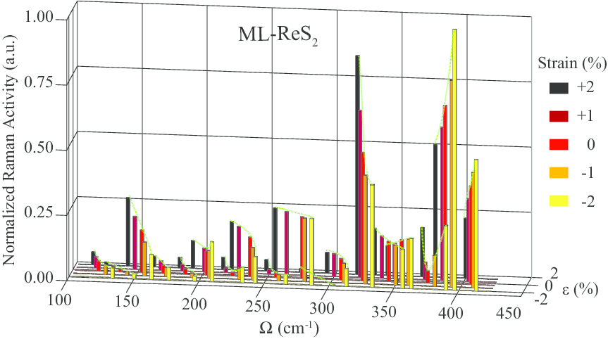
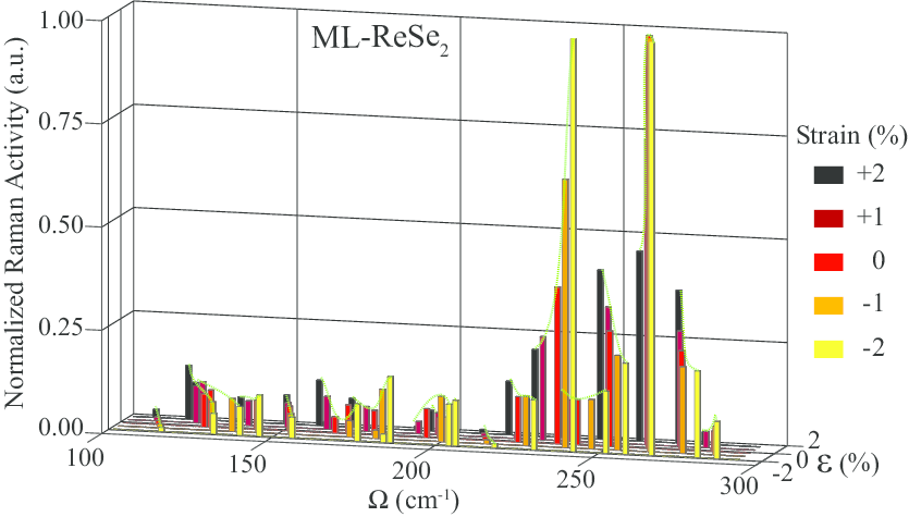
In the case of single-layer ReSe2, the frequencies of the Raman active modes significantly soften when compared with those of ReS2 due to lower in-plane stiffness of the crystal. The highest Raman active mode has a frequency of 290.7 cm-1. The Ag-like phonon modes of Re atoms have the frequencies of 106.5 and 116.0 cm-1 while the frequencies are 157.0 and 176.2 cm-1 for that of Se atoms. The most significant response of the Raman activity is found for the most intense peak at 260.9 cm-1. Under compressive strain, the activity of the coupled mode of Re and Se atoms increases about 50% of its unstrained value while it decreases about 55% under tensile biaxial strain. Although, in some of the Raman active modes display significant changes under strain, due to the rigidity of the ReX2 crystals they are almost irresponsive to the applied strain.
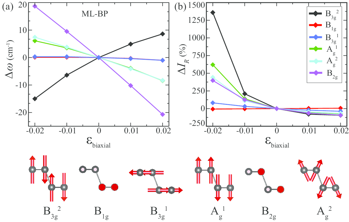
III.4.2 Black Phosphorus Single-Layer Crystal
Single-layer bp is a recently synthesized, in-plane anisotropic member of 2D single-layer family. It is known to posses remarkable in-plane anisotropic electrical, optical and phonon properties3 ; 4 ; 5 . There are 4 P atoms in its rectangular primitive unit cell and its crystal structure belongs to space group.
Phonon-band structure of single-layer bp demonstrates that 12 phonon branches exist (see Fig. 2(d)). According to the group theory analysis, it exhibits 6 Raman active phonon modes known as B1g, B, A, B, B2g, and A. The Raman active modes, B1g, B, and B2g, represent the in-plane vibration of P atoms while B, A, and A represent out-of-plane motion. Experimental measurements revealed that only 3 of the 6 Raman active modes (A, B2g, and A) exhibit prominent Raman intensitybp-1 ; bp-2 . The frequencies of the 3 prominent peaks are 352.1, 424.2, and 455.2 cm-1 for A, B2g, and A, respectively. For the unstrained single-layer bp, Raman activities demonstrate that the A and A have much higher activities than that of B2g which was also observed in the experimentbp-1 ; bp-2 .
| (cm-1) | (%) | |||
|---|---|---|---|---|
| A | 352.1 | 1.05 | 0.53 | |
| B2g | 559.6 | 2.32 | 1.16 | |
| A | 296.8 | 0.87 | 0.44 |
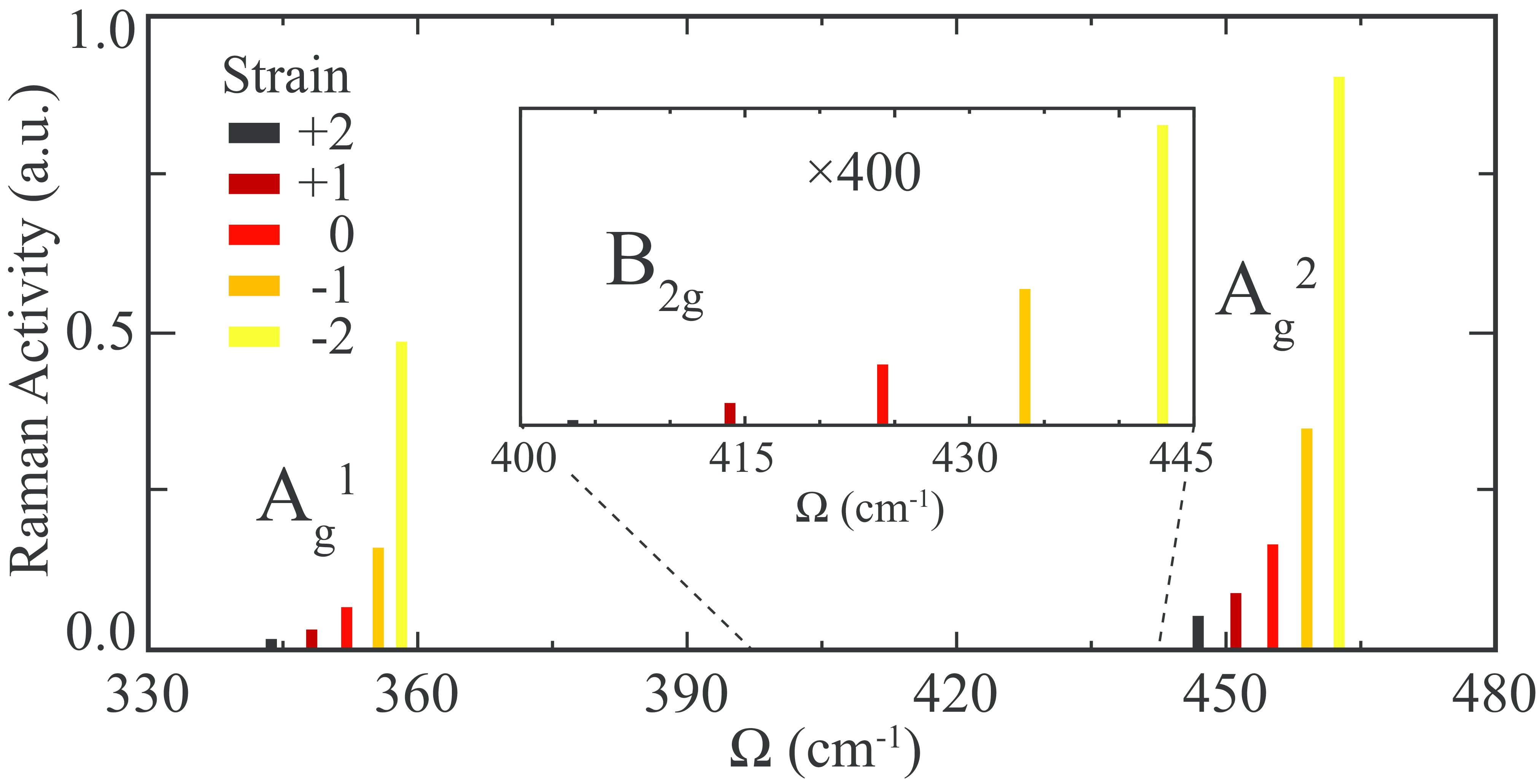
It was shown by Fei et al. that the frequencies of vibrational modes of and their Raman scattering peaks in black phosphorus exhibit substantial and distinct shifts according to the strength of applied uiaxial strainfei-hakem . Here we investigate response of the frequencies and Raman signals to the applied biaxial strain. When single-layer bp is biaxially compressed up to 2%, the frequency of A phonon mode displays a hardening from 455.2 to 462.6 cm-1 while a softening to 446.9 cm-1 is found under 2% tensile biaxial strain. The frequency of B2g phonon mode displays the same trend as the A mode under biaxial strain. A softening to 403.5 cm-1 and a hardening to 442.9 cm-1 are seen for the frequency of B2g phonon mode under tensile and compressive strains, respectively. For the strain range of 2%, the response of frequency of B2g is much larger than that of A mode. Another characteristic Raman active mode of single-layer bp is A which represents the out-of-plane vibrations of the P atoms in upper and lower sublayers in opposite directions. The frequency of the mode softens to 343.7 cm-1 under 2% of tensile strain while it hardens to 358.2 cm-1 under that of compressive strain. The responses of peak frequencies of the 3 prominent modes to the applied in-plane biaxial strain are compared through their mode Gruneissen parameters given in Table 3. The greater is calculated for B2g mode which exactly has the in-plane vibrational characteristic. The values of A and A are smaller than that of B2g since they both demonstrate the out-of-plane vibration of P atoms.
The Raman activity of A phonon mode is highly affected by the applied strain. The Raman activity of A increases up to 5.4 (440%) of its unstrained value under 2% of compressive strain. However, its Raman activity is less sensitive to tensile strain when compared with that of compressive strain. Under 2% of tensile strain, the Raman activity decreases about 68% of its initial value which is much lower than that of compressive value. In addition, the Raman activity of B2g phonon mode is approximately 375 times smaller than that of A mode for the unstrained crystal structure. The Raman activity of B2g displays a symmetric response under compressive and tensile biaxial strains. Due to the out-of-plane nature of the mode, the same trend is also illustrated for B2g mode. The Raman activity of A phonon mode is in the order of that of A mode in unstrained structure. Since the two modes display the same trend under biaxial strain, it is meaningful to compare the Raman activity of A with its unstrained value. When 2% of compressive strain is applied, the Raman activity of A increases about 7 times of its unstrained value.
As mentioned above, totally 6 Raman active modes exist for single-layer bp 3 of which have very low Raman activities (at the order of 10-5 of the value of A mode). The frequencies of B1g and B are 193.8 and 232.8 cm-1, respectively. We find that both the frequencies and the corresponding Raman activities are mostly insensitive to the applied biaxial strain. The reason is the vibrational characteristic of the modes. It is seen that the modes represent in-plane vibration of P atoms. Differing from B2g, in B1g and B P atoms located at the same layer vibrate in the same direction. As the biaxial strain is applied, the thickness of the layer decreases but the out-of-plane symmetry of the vibrating atoms is mostly conserved. Thus, both peak positions and Raman activities mostly remain unaffected by the applied strain.
IV Conclusions
In this study, the first-order off-resonant Raman spectra of 2D single-layers of monoatomic (graphene, Si, and Ge), diatomic (h-BN, h-AlN, and h-GaN), in-plane isotropic TMDs (MoS2, MoSe2, WS2, and WSe2), and in-plane anisotropic crystals (ReS2, ReSe2, and bp) and their strain-dependent behaviors were investigated by performing DFT-based calculations. Our results well fit into the reported experimental results for the first-order off-resonant Raman activities. In addition, the effect of biaxial strain on Raman spectra of the single-layer crystals was analyzed in terms of their peak frequencies and corresponding Raman activities. Our findings can be summarized as follows; (i) strain can be directly observed in Raman scattering experiments by the knowledge of the peak positions of Raman active phonon modes, (ii) the A-peak of the single-layer Si and Ge disappear under sufficient tensile strain, (iii) especially in mono and diatomic single-layers, the shift of the peak frequencies is stronger indication of the strain rather than the change in Raman activities, (iv) in the case of isotropic single-layer TMDs (MoS2, MoSe2, WS2, and WSe2) the activity ratio of E to A1 phonon mode, , is a key for the determination of the induced strain since the ratio significantly increases when a tensile strain is applied while it decreases under compressive strain due to the opposite responses of the phonon modes, and (v) finally, a remarkable point for the anisotropic single-layers of ReX2 is that there is no significant change in Raman activities under biaxial strain.
In general, it was confirmed by the calculations that to extract strain information in novel single-layer 2D crystals, peak positions of lattice vibrational modes and the corresponding Raman activities are useful.
Acknowledgements.
Computational resources were provided by TUBITAK ULAKBIM, High Performance and Grid Computing Center (TR-Grid e-Infrastructure). H.S. acknowledges financial support from the Scientific and Technological Research Council of Turkey (TUBITAK) under the project number 116C073.References
- (1) K. S. Novoselov, A. K. Geim, S. V. Morozov, D. Jiang, Y. Zhang, S. V. Dubonos, I. V. Grigorieva, and A. A. Firsov, Science 306, 666 (2004).
- (2) Q. H. Wang, K. Kalantar-Zadeh, A. Kis, J. N. Coleman, and M. S. Strano, Nature Nanotech. 7, 699 (2012).
- (3) G. R. Bhimanapati , Z. Lin , V. Meunier , Y. Jung , J. Cha , S. Das , D. Xiao , Y. Son , M. S. Strano , V. R. Cooper , L. Liang , S. G. Louie , E. Ringe , W. Zhou , S. S. Kim , R. R. Naik , B. G. Sumpter , H. Terrones , F. Xia , Y. Wang , J. Zhu , D. Akinwande , N. Alem , J. A. Schuller , R. E. Schaak , M. Terrones, and J. A. Robinson , ACS Nano. 9 (12), 11509 (2015).
- (4) D. Akinwande , N. Petrone, and J. Hone, Nat. Commun. 5, 5678 (2014).
- (5) K. F. Mak, C. Lee, J. Hone, J. Shan, and T. F. Heinz, Phys. Rev. Lett. 105, 136805 (2010).
- (6) R. A. Gordon, D. Yang, E. D. Crozier, D. T. Jiang, and R. F. Frindt, Phys. Rev. B 65, 125407 (2002).
- (7) J. N. Coleman, M. Lotya, A. O’Neill, S. D. Bergin, P. J. King, U. Khan, K. Young, A. Gaucher, S. De, R. J. Smith, I. V. Shvets, S. K. Arora, G. Stanton, H. Y. Kim, K. Lee, G. T. Kim, G. S. Duesberg, T. Hallam, J. J. Boland, J. J. Wang, J. F. Donegan, J. C. Grunlan, G. Moriarty, A. Shmeliov, R. J. Nicholls, J. M. Perkins, E. M. Grieveson, K. Theuwissen, D. W. McComb, P. D. Nellist, and V. Nicolosi, Science 331, 568 (2011).
- (8) J. S. Ross, P. Klement, A. M. Jones, N. J. Ghimire, J. Yan, D. G. Mandrus, T. Taniguchi, K. Watanabe, K. Kitamura, W. Yao, D. H. Cobden, and X. Xu, Nature Nanotech. 9, 268 (2014).
- (9) H. Sahin, S. Tongay, S. Horzum, W. Fan, J. Zhou, J. Li, J. Wu, and F. M. Peeters, Phys. Rev. B 87, 165409 (2013).
- (10) S. Tongay, H. Sahin, C. Ko, A. Luce, W. Fan, K. Liu, J. Zhou, Y.S. Huang, C.H. Ho, J. Yan, D. F. Ogletree, S. Aloni, J. Ji, S. Li, J. Li, F. M. Peeters, and J. Wu, Nat. Comm. 5, 3252 (2014).
- (11) S. Horzum, D. Cakir, J. Suh, S. Tongay, Y.S. Huang, C.H. Ho, J. Wu, H. Sahin, and F. M. Peeters, Phys. Rev. B 89, 155433 (2014).
- (12) B. Chen, H. Sahin, A. Suslu, L. Ding, M. I. Bertoni, F. M. Peeters, and S. Tongay, ACS Nano 9(5), 5326 (2015).
- (13) M. Yagmurcukardes, E. Torun, R. T. Senger, F. M. Peeters, and H. Sahin Phys. Rev. B 94, 195403 (2016).
- (14) A. Kara, H. Enriquez, A. P. Seitsonen, L. C. L. Y. Voon, S. Vizzini, B. Aufray, and Hamid Oughaddou, Surf. Science Report. 67, 1 (2012).
- (15) S. Cahangirov, M. Topsakal, E. Akturk, H. Sahin, and S. Ciraci, Phys. Rev. Lett. 102, 236804 (2009).
- (16) H. Sahin, S. Cahangirov, M. Topsakal, E. Bekaroglu, E. Akturk, R. T. Senger, and S. Ciraci, Phys. Rev. B 80, 155453 (2009).
- (17) Q. Wang, Q. Sun, P. Jena, and Y. Kawazoe, ACS Nano 3, 621 (2009).
- (18) K. K Kim, A. Hsu, X. Jia, S. M. Kim, Y. Shi, M. Hofmann, D. Nezich, J. F. Rodriguez-Nieva, M. Dresselhaus, T. Palacios, and J. Kong, Nano Lett. 12 (1), 161 (2012).
- (19) P. Tsipas, S. Kassavetis, D. Tsoutsou, E. Xenogiannopoulou, E. Golias, S. A. Giamini, C. Grazianetti, D. Chiappe, A. Molle, M. Fanciulli, and A. Dimoulas, Appl. Phys. Lett. 103, 251605 (2013).
- (20) C. Bacaksiz, H. Sahin, H. D. Ozaydin, S. Horzum, R. T. Senger, and F. M. Peeters, Phys. Rev. B 91, 085430 (2015).
- (21) D. Chenet, B. Aslan, P. Huang, C. Fan, A. van der Zande, T. Heinz, and J. Hone, Nano Lett. 15, 5667 (2015).
- (22) L. Hart, S. Dale, S. Hoye, J. Webb, and D. Wolverson, Nano Lett. 16, 1381 (2016).
- (23) M. Yagmurcukardes, C. Bacaksiz, R. T. Senger, and H. Sahin, 2D Materials 4, 035013 (2017).
- (24) S. Yang, S. Tongay, Y. Li, Q. Yue, J.-B. Xia, S.-S. Li, J. Li, and S.-H. Wei, Nanoscale 6, 7226 (2014).
- (25) S. Yang, S. Tongay, Q. Yue, Y. Li, B. Li, and F. Lu, Sci. Rep. 4, 5442 (2014).
- (26) J. Qiao, X. Kong, Z. X. Hu, F. Yang, and W. Ji, Nat. Commun. 5, 4475 (2014).
- (27) F. Xia, H. Wang, and Y. Jia, Nat. Commun. 5, 4458 (2014).
- (28) R. Fei and L. Yang, Nano Lett. 14, 2884 (2014).
- (29) C. V. Raman, Indian J. Phys. 2, 387 (1928).
- (30) A. C. Ferrari, J. C. Meyer, V. Scardaci, C. Casiraghi, M. Lazzeri, F. Mauri, S. Piscanec, D. Jiang, K. S. Novoselov, S. Roth, A. K. Geim, Phys. Rev. Lett. 97, 187401 (2006).
- (31) X.-F. Qiao, X.-L. Li, X. Zhang, W. Shi, J.-B. Wu, T. Chen and P.-H. Tan, Appl. Phys. Lett. 106, 223102 (2015).
- (32) X. Zhang, W. P. Han, J. B. Wu, S. Milana, Y. Lu, Q. Q. Li, A. C. Ferrari, P. H. Tan, Phys. Rev. B 87, 115413 (2013).
- (33) P. H. Tan, W. P. Han, W. J. Zhao, Z. H. Wu, K. Chang, H. Wang, Y. F. Wang, N. Bonini, N. Marzari, N. Pugno, G. Savini, A. Lombardo, A. C. Ferrari, Nat. Mater. 11, 294 (2012).
- (34) J.-B. Wu, X. Zhang, M. Ijas, W.-P. Han, X.-F. Qiao, X.-L. Li, D.-S. Jiang, A. C. Ferrari, P.-H. Tan, Nat Comm. 5, 5309 (2014).
- (35) J.-B. Wu, Z.-X. Hu, X. Zhang, W.-P. Han, Y. Lu, W. Shi, X.-F. Qiao, M. Ijias, S. Milana, W. Ji, A. C. Ferrari, P.-H. Tan, ACS Nano 9, 7440 (2015).
- (36) Ph. Colomban, Spectroscopy Europe 15, 8 (2003).
- (37) G. Gouadec, Ph. Colomban, Prog. Cryst. Growth Charact. Mater. 53, 1 (2007).
- (38) M. Havel, D. Baron, Ph. Colomban, J. Mater. Sci. 39, 6183 (2004).
- (39) X. Zhang, X.-F. Qiao, W. Shi, J.-B. Wu, D.-S. Jiang, and P.-H. Tan, Chem. Soc. Rev. 44, 2757 (2015).
- (40) F. Guinea, M. I. Katsnelson, and A. K. Geim, Nat. Phys. 6, 30 (2009).
- (41) K. He, C. Poole, K. F. Mak, J. Shan, Nano Letters 13, 2931 (2013).
- (42) Z. H. Ni, T. Yu, Y. H. Lu, Y. Y. Wang, Y. P. Feng and Z. X. Shen, ACS Nano 2, 2301 (2008).
- (43) M. Huang, H. Yan, T. F. Heinz, and J. Hone, Nano Lett. 10, 4074 (2010).
- (44) A. C. Ferrari, and D. M. Basko, Nat. Nanotech. 8, 235 (2013).
- (45) A. Berkdemir, H. R. Gutiérrez, A. R. Botello-Méndez, N.Perea-López, A. L. Elíías, C.-I. Chia, B. Wang, V. H. Crespi, F. López-Urías, J.-C. Charlier, H. Terrones, and Mauricio Terronesa, Sci. Rep. 3, 1755 (2013).
- (46) D. A. Chenet, O. B. Aslan, P. Y. Huang, C. Fan, A. M. van der Zande, Tony F. Heinz, and J. C. Hone, Nano Lett. 15, 5667 (2015).
- (47) H. Frostig, T. Bayer, N. Dudovich, Y. C. Eldar, Y. Silberberg, Nat. Photon. 9, 339 (2015).
- (48) G. Kresse and J. Hafner, Phys.Rev.B 47, 558 (1993).
- (49) G. Kresse and J. Furthmuller, Phys.Rev.B 54, 11169 (1996).
- (50) J. P. Perdew, K. Burke, and M. Ernzerhof, Phys. Rev. Lett. 77, 3865 (1996).
- (51) S. J. Grimme, J. Comput. Chem. 27, 1787 (2006).
- (52) G. Henkelmana, A. Arnaldssonb, H. Jónsson, Comput. Mater. Sci. 36, 354 (2006).
- (53) J. P. Perdew and A. Zunger, Phys. Rev. B 23 (10), 5048 (1981).
- (54) D. M. Ceperley and B. J. Alder, Phys. Rev. Lett. 45, 566 (1980).
- (55) Z. Y. Al Balushi, K. Wang, R. K. Ghosh, R. A. Vilá, S. M. Eichfeld, J. D. Caldwell, X. Qin, Y.-C. Lin, P. A. DeSario, G. Stone, S. Subramanian, D. F. Paul, R. M. Wallace, S. Datta, J. M. Redwing, and J. A. Robinson, Nat. Mater. 15, 1166 (2016).
- (56) S. Tongay, H. Sahin, C. Ko, A. Luce, W. Fan, K. Liu, J. Zhou, Y. S. Huang, C. H. Ho, J. Y. Yan, D. F. Ogletree, S. Aloni, J. Ji, S. S. Li, J. B. Li, F. M. Peeters, and J. Q. Wu, Nat. Commun. 5, 3252 (2014).
- (57) Y. Feng, W. Zhou, Y. Wang, J. Zhou, E. Liu, Y. Fu, Z. Ni, X. Wu, H. Yuan, F. Miao, B. Wang, X. Wan, D. Xing, Phys. Rev. B 92, 054110 (2015).
- (58) L. Li, Y. Yu, G. J. Ye, Q. Ge, X. Ou, H. Wu, D. Feng, X. H. Chen, and Y. Zhang, Nat. Nanotech. 9, 372 (2014).
- (59) F. Xia, H. Wang, and Y. Jia, Nat. Commun. 5, 4458 (2014).
- (60) H. O. H. Churchill, and P. J.-Herrero, Nat. Nanotech. 9, 330 (2014).
- (61) X. Wang, A. M. Jones, K. L. Seyler, V. Tran, Y. Jia, H. Zhao, H. Wang, L. Yang, X. Xu, and F. Xia, Nat. Nanotech. 10, 517 (2015).
- (62) A. Favron, E. Gaufres, F. Fossard, A.-L. P.-L’Heureux, N. Y-W. Tang, P. L. Levesque, A. Loiseau, R. Leonelli, S. Francoeur, and R. Martel, Nat. Mater. 14, 826 (2015).
- (63) R. Fei and L. Yang, Appl. Phys. Lett. 105, 083120 (2014).
- (64) M. Gmitra, S. Konschuh, C. Ertler, C. Ambrosch-Draxl, and J. Fabian, Phys. Rev. B 80, 235431 (2009).
- (65) C. J. Tabert and E. J. Nicol, Phys. Rev. B 87, 235426 (2013).
- (66) C.-C. Liu, W. Feng, and Y. Yao, Phys.Rev.Lett. 107, 076802 (2011).
- (67) C.-C. Liu, H. Jiang, and Y. Yao, Phys. Rev. B 84, 195430 (2011).
- (68) R. D’Souza and S. Mukherjee Phys. Rev. B 95, 085435 (2017).
- (69) G. Kern, G. Kresse, and J. Hafner Phys. Rev. B 59, 8551 (1999).
- (70) D. Doratotaj, J. R. Simpson, and J.-A. Yan Phys. Rev. B 93, 075401 (2016).
- (71) C. Rice, R. J. Young, R. Zan, U. Bangert, D. Wolverson, T. Georgiou, R. Jalil, and K. S. Novoselov, Phys. Rev. B 87, 081307 (2013).
- (72) K. K. Kim, A. Hsu, X. Jia, S. M. Kim, Y. Shi, M. Dresselhaus, T. Palacios, and J. Kong, ACS Nano 6, 8583 (2012).
- (73) F. Huser, T. Olsen, and K. S. Thygesen, Phys. Rev. B 88, 245309 (2013).
- (74) A. Ramasubramaniam, Phys. Rev. B 86, 115409 (2012).
- (75) N. Dong, Y. Li, Y. Feng, S. Zhang, X. Zhang, C. Chang, J. Fan, L. Zhang, and J. Wang, Sci. Rep. 5, 14646 (2015).