Point-projection microscopy of nano-localized photoemission currents at sub-40 femtosecond time scales
Abstract
Femtosecond point-projection microscopy (fs-PPM) is an electron microscopy technique that possesses a combination of high spatio-temporal resolution and sensitivity to local electric fields. This allows it to visualize ultrafast charge carrier dynamics in complex nanomaterials. We benchmark the capability of the fs-PPM technique by imaging the ultrafast dynamics of charge carriers produced by multiphoton ionization of silver nanowires. The space-charge driven motion of photoelectrons is followed on sub-100 nm length scales, while the dynamics are captured on 30–100 fs time scales. The build-up of electron holes in the silver nanowires following photoelectron ejection, i.e. positive charging, has also been observed. The fastest observed photoelectron temporal response is 33 fs (FWHM), which represents an upper estimate of the instrument response function and is consistent with an expected electron wavepacket duration of 13 fs based on simulations.
The functionality of a nanomaterial is inherently linked to the composition and structure of its nanoscale building blocks, e.g. quantum dots Nozik et al. (2010), nanowires Hu et al. (1999) and/or 2D materials Geim and Grigorieva (2013). The interplay between structure and charge transport at the nanoscale in these complex systems often plays a crucial role in the development of new technological devices and applications. Directly visualizing charge carrier motion in these systems requires a technique that ideally possesses femtosecond temporal resolution, nanometer spatial resolution, and a high sensitivity to excited charge carrier populations. Over the past few decades powerful ultrafast microscopy techniques have been developed that have, to varying extents, realized this combination of extreme requirements.
Optical pump-probe microscopy and spectroscopy Grumstrup et al. (2015) have, for example, been extensively used to study charge carrier generation and propagation in many diverse and technologically relevant systems Gundlach and Piotrowiak (2009); Grumstrup et al. (2014); Seo et al. (2016); Grancini et al. (2012); Guo et al. (2017). The temporal resolution of ultrafast optical microscopy is fundamentally only limited by the optical probe pulse duration, which can be well below 10 fs. However, the attainable spatial resolution is limited by the wavelength of light and is, consequently, on the order of a few hundred nanometer. Using near-field confinement Kravtsov et al. (2016), or decreasing the wavelength of the light into the XUV Zhang et al. (2015); Tadesse et al. (2016) or soft X-ray spectral range Fischer et al. (2006), it is possible to improve the spatial resolution of optical pump-probe imaging techniques down to 10 nm.
A fundamentally different approach is taken by ultrafast microscopy techniques that employ electrons as probes. The inherently small de Broglie wavelength of electrons in principle enables achieving a spatial resolution well beyond that of optical microscopy techniques. For example, time-resolved photoelectron emission microscopy has achieved spatial resolutions on the order of few tens of nm and a temporal resolution equivalent to that of optical microscopy techniques Kubo et al. (2005); Meyer zu Heringdorf et al. (2007); Man et al. (2016); Da̧browski et al. (2016). Techniques that seek to expand conventional scanning and transmission electron microscopy to the femtosecond regime and are capable of visualizing nanoscale carrier motion have also been demonstrated Zewail (2010); Barwick et al. (2009); Najafi et al. (2015); Feist et al. (2017); Liao et al. (2017); da Silva et al. (2017). A major challenge for the latter approach has been the dispersive and space-charge induced electron pulse spreading during propagation through the electron optical column of the microscope. This currently limits the achievable temporal resolution to the few hundred femtosecond range, though techniques based on coherent electron-light interactions have been demonstrated that could enable electron microscopy with attosecond temporal resolution in the future Priebe et al. (2017); Morimoto and Baum (2017).
An attractive alternative for achieving nanometer spatial and femtosecond temporal resolution using electrons as probes is femtosecond point-projection microscopy (fs-PPM) Quinonez et al. (2013); Müller et al. (2014); Bainbridge et al. (2016). The combination of a nanotip electron source and lens-less imaging allows for a temporal resolution comparable to ultrafast optical microscopy and a spatial resolution that can, in principle, reach the single nm level Longchamp et al. (2017); Paarmann et al. (2012); Vogelsang et al. (2015); Müller et al. (2016). Due to the use of low-energy, i.e. sub-1 kV, electrons, fs-PPM is highly sensitive to local electric fields Beyer and Gölzhäuser (2010), which makes it especially well suited to visualizing charge carrier separation and dynamics Müller et al. (2014). The first experimental studies with fs-PPM were applied to imaging surface photovoltage dynamics in semiconductor nanowires Müller et al. (2014) and photoelectron generation from nanotips Bainbridge et al. (2016). These initial experiments established the capability of the fs-PPM technique to reach sub-100 nm spatial resolution, while imaging charge carrier dynamics on a 100 fs timescale. However, though simulations have indicated a temporal resolution comparable to the optical excitation pulse duration, so far the experiments employing fs-PPM have not demonstrated experimentally the capability of the technique to image sub-100 fs dynamics and were either limited by the slow sample system dynamics Müller et al. (2014), or by the large tip-sample distance Bainbridge et al. (2016) and the resulting long electron pulse durations.
In this paper, we report a benchmark experiment that visualizes dynamics that are considerably faster than what has been shown so far with this technique, illustrating the potential of fs-PPM in combining nanoscale spatial and femtosecond temporal resolution in imaging charge carrier dynamics. The multiphoton ionization and subsequent space-charge driven dynamics of photoelectrons emitted from silver nanowires is captured on timescales as low as 33 fs. It is also shown that the dynamics are highly dependent on the sample structure and that they vary on a sub-100 nm scale, demonstrating the advantage of combining nanometer spatial and femtosecond temporal resolution.
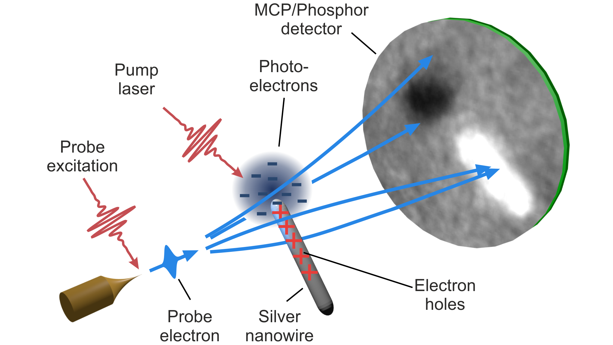
A schematic illustration of the experimental setup is shown in Fig. 1. In PPM a nanotip that acts as a point-like source of electrons is brought close to the sample such that the diverging electron beam projects a magnified image of the sample onto the detector Morton and Ramberg (1939); Spence et al. (1993). In fs-PPM the imaging electrons are generated by focusing an ultrashort laser pulse on the apex of a metallic nanotip, which leads to non-linear photoemission of an ultrashort electron pulse. The combination of a nanotip source and lens-less imaging allows for an ultra-compact microscope column, where the distance from the electron source to the sample is on the micrometer scale. This minimizes the effect of dispersive broadening and allows for an electron pulse duration comparable to that of the optical excitation pulse Paarmann et al. (2012). It is important to note that the projection image produced by the electron beam is not merely a geometric projection of the sample, but contains information on electric fields at the sample through lensing effects Beyer and Gölzhäuser (2010); Lai et al. (1999). Local fields cause the imaging (probe) electrons to be deflected while passing by the sample and result in the appearance of bright or dark features in the projected image, depending on whether the electrons are attracted or repelled by those fields (see Fig. 1).
The experiment was performed using a pump-probe scheme, in which an ultrashort laser pulse excites the sample, photoionizing the silver nanowires, and a time-delayed electron pulse records an ultrafast image of the nanoscale system. Laser pulses of 8 fs duration at 800 nm and a repetition rate of 1 MHz were used for the experiment, with pump and probe excitation pulse energies of and , respectively. Both laser pulses were focused onto the sample and tip apex by silver parabolic mirrors, reaching estimated fluences of and , respectively. In order to facilitate optical access of the probe excitation laser pulse to the nanotip the sample was inclined with respect to the nanotip by . The imaging electrons were accelerated by a tip voltage of -207 V, while the sample was kept at ground potential. The tip-sample distance was , resulting in a geometric magnification factor of 5000, and was chosen such that there was no observable photoelectron generation from the nanotip by the pump pulse, while at the same time minimizing the propagation distance for the electron pulse. Silver nanowires (Sigma-Aldrich) with a nominal diameter of and a length of were deposited from a colloidal solution onto a lacey carbon transmission electron microscopy grid by dropcasting.
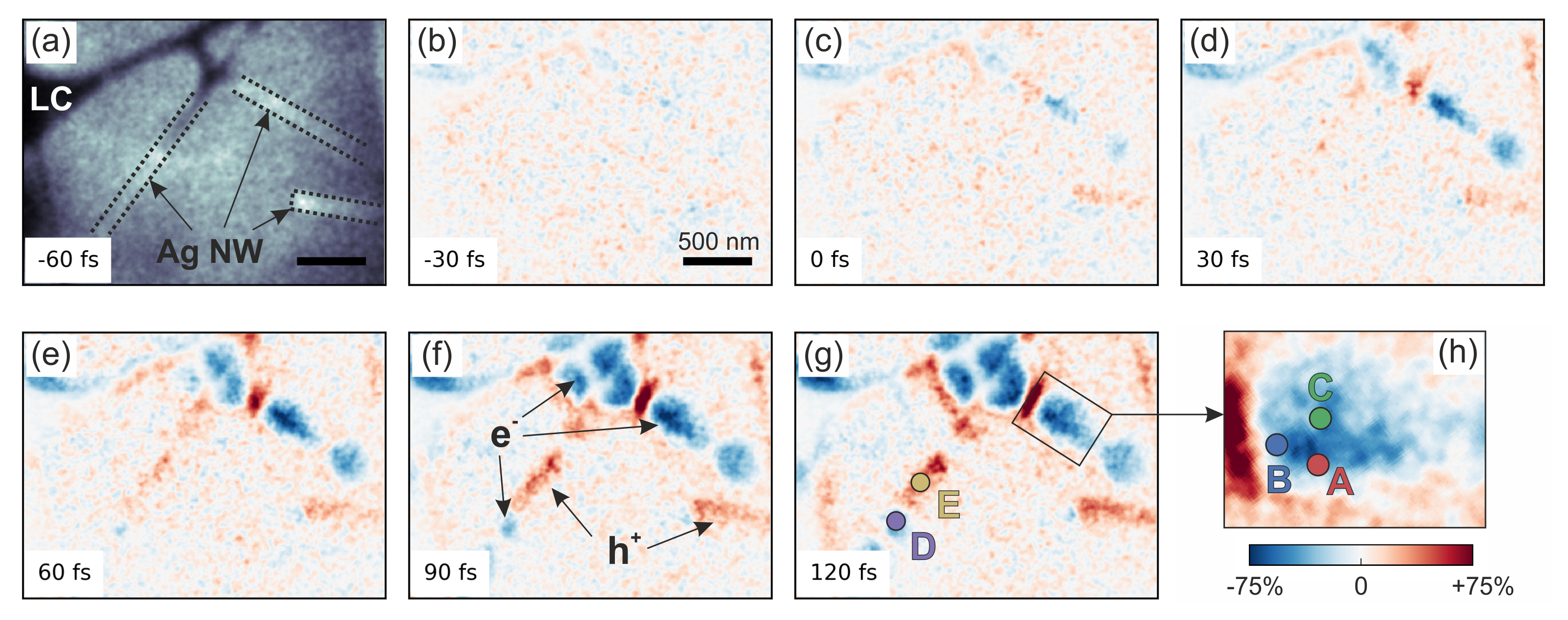
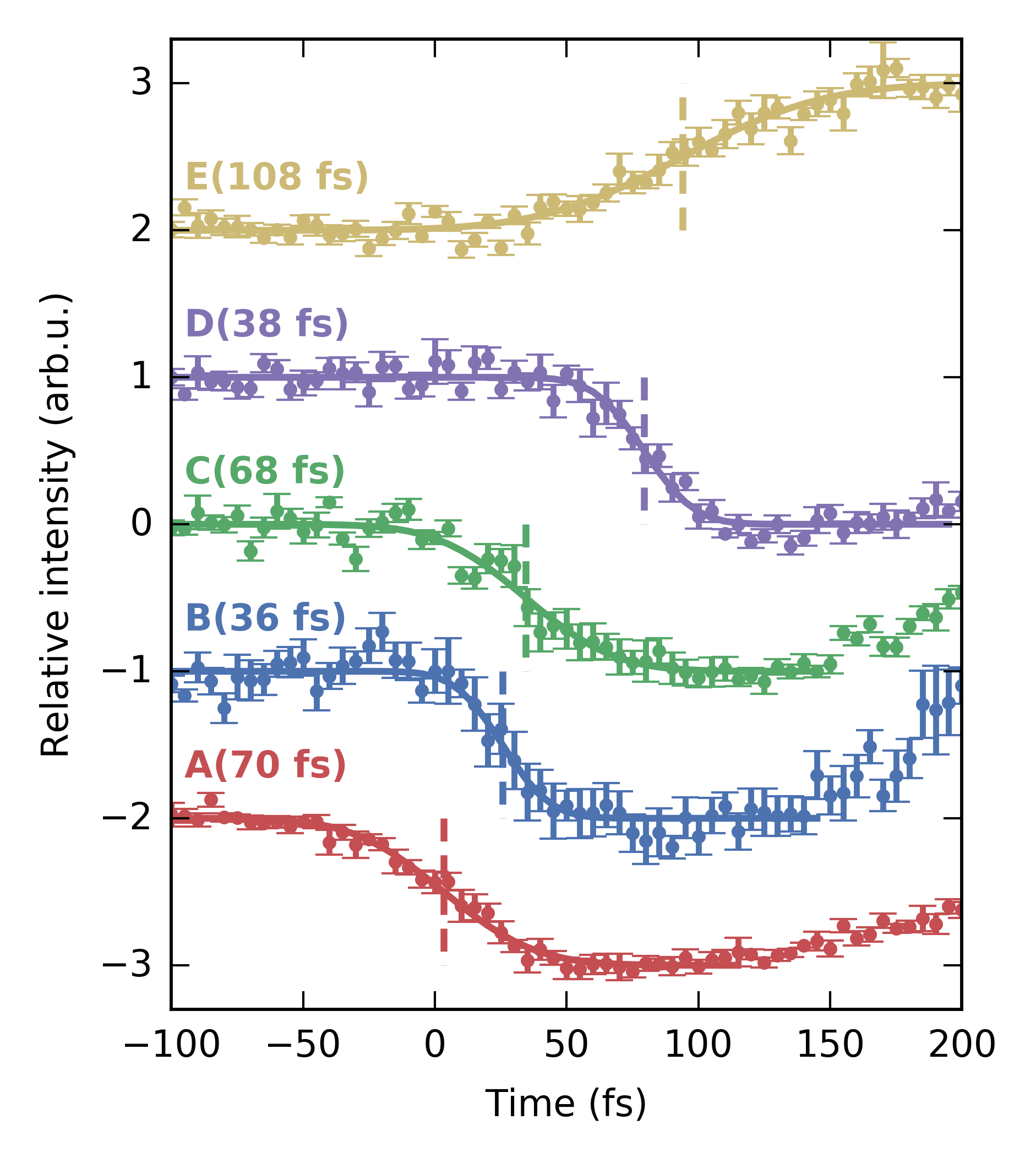
Figure 2 shows an experimental pump-probe time-sequence, where frames (b)–(g) show difference images with respect to the reference image (a) of the sample before photoexcitation. The silver nanowires are visible in the reference image as bright stripes, due to the presence of static electric fields that lead to the formation of an electron biprism lens Beyer and Gölzhäuser (2010); Lai et al. (1999). After photoexcitation, locations with strong photoelectron emission are clearly visible in the difference images as regions with transiently reduced transmission, e.g. blue color regions annotated with e- in Fig. 2(f). In this case the presence of the photoelectrons leads to a locally repelling electric field on the imaging electrons that acts as a negative lens and causes a reduction of up to 75% of the intensity in the projected image. Besides the strong transient suppression of the signal in regions where photoelectrons are emitted, the positive charging of the nanowires themselves can be observed as well, e.g. red color regions indicated by h+ in Fig. 2(f). The positive charging of the nanowires upon emission of photoelectrons leads to an enhancement of the electron biprism effect and therefore to an increase in their apparent brightness in the projection images. Finally, we point out that in the difference image time-sequence the dynamics in the top right corner of the images appears to start sooner than in the lower left corner. In Fig. 2(c) clear photoelectron emission signatures can be seen in the top right corner, whereas the first onset of photoelectron emission in the lower left corner only becomes visible in frame (e), after a 60 fs delay. This effect can be attributed to propagation path length differences that result from the inclination of the sample with respect to the probing electron beam, and the geometric curvature of the electron probe pulses produced by the the point-like electron source Paarmann et al. (2012). Due to the low velocity of the probe electrons there can be a considerable time delay in the arrival of the probe pulse across the sample, which causes an effective shift of the time zero across the field-of-view.
We now investigate the dynamic behavior at a few exemplary positions in more detail, labeled as points A–E in Fig. 2(g) and (h). The time response at these points is shown in Fig. 3, together with fitted error-function curves (solid lines) of the form . For each curve the full width at half maximum (FWHM) time of the Gaussian distribution corresponding to the fitted standard deviation is indicated in brackets, while the fitted time zero is marked by a vertical dashed line. First, we observe that the time constants show a rather large spread in values: at points B and D we find fs, whereas at points A, C and E it varies between fs. In particular, we observe that the positively charging nanowires (point E) have a dynamic response that is much slower than that of the photoelectrons. This is because the former involves hole propagation within the nanowire, whereas the latter is due to the propagation of photoelectrons driven by strong space-charge forces resulting from the high photoemission densities under the current experimental conditions. Second, we see a clear shift in the fitted time zero at each position. These time zero shifts can be attributed to two distinct effects: (1) probe electron path length differences, which were pointed out previously, and (2) charge carrier propagation effects. The 80 fs time zero shift between points A and D, which are apart in the sample plane, can largely be explained by the first effect. However, points A, B and C are separated by 100 nm from each other, such that probe path length difference effects can only account for a time zero difference of less than 4 fs. The time zero shifts between curves A, B and C, which are on the order of few tens of fs, can therefore be attributed to photoelectron propagation effects.
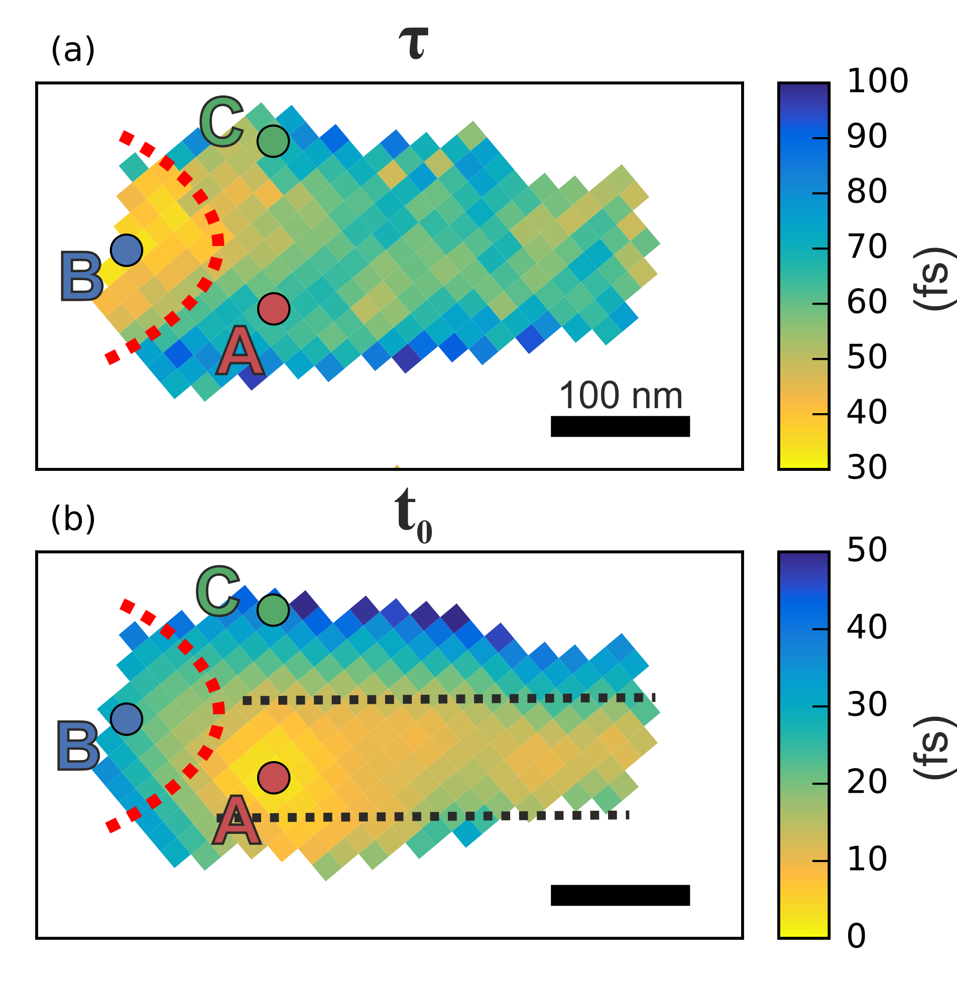
In order to study photoelectron emission and propagation dynamics in the immediate vicinity of the nanowires we show in Fig. 4 a map of the time constants () and time zeros () for the entire region indicated in Fig. 2(h). The fitting constants are obtained from error-function fits, such as those shown in Fig. 3, at a regular grid within in the region of interest. In the time constant map in Fig. 4(a) we indeed see that the speed of the photoelectron dynamics is spatially inhomogeneous; the time constants of the dynamics in the small 100 nm region to the left of the dashed red line are 30–40 fs, while in the region to the right they are in the range of 40–100 fs. Furthermore, the expansion and propagation of the photoelectron charge distribution can be observed directly in the time zero map in Fig. 4(b). The position of the nanowire itself is visible as a rather uniform region with very low time zero values of 0–15 fs located between the black dashed lines. Outside of this region there is a clear gradient in the extracted time zero values, with values of 15–50 fs, that is attributed to the space-charge induced propagation of the photoelectrons away from the emission point at the nanowire. This highly inhomogeneous nature of photoelectron dynamics taking place on sub-100 nm length and sub-40 fs time scales clearly illustrates the usefulness of the combination of high temporal and spatial resolution realized with the fs-PPM technique.
Finally, we address the relation between the temporal resolution and the observed photoelectron dynamics in the current experiment. Space-charge effects are frequently used as a cross-correlation tool for evaluating the temporal resolution of femtosecond electron diffraction and microscopy techniques Dolocan et al. (2006); Dwyer et al. (2006); Hebeisen et al. (2008); Centurion et al. (2008); Bainbridge et al. (2016). Disregarding intrinsic photoelectron emission dynamics, the lowest time constants observed in the current experiment provide us with an upper limit on the instrument response function of 33 fs (FWHM). In the single electron per pulse regime the fs-PPM setup was operated for this experiment, the probe electron pulse duration at the sample is determined by dispersive pulse broadening only. An estimate of the dispersive pulse broadening for current experimental conditions was obtained using a particle tracing model that simulates the spread in arrival times of on-axis probe electrons with different initial energies Müller et al. (2016); Paarmann et al. (2012). Assuming an initial energy spread of 0.75 eV Quinonez et al. (2013); Yanagisawa et al. (2011) we obtain a pulse duration at the sample of 13 fs (FWHM). Another important factor that affects the effective time resolution of the fs-PPM setup is the traversal time of the low energy probe electrons through the interaction volume in the sample plane. Two factors that influence this are the sample system extent in the electron beam propagation direction (60 nm) and mechanical vibrations between the tip and sample (100 nm), which contribute an estimated additional 12 fs to the effective temporal resolution. Increasing the mechanical stability of the setup is therefore expected to improve both the temporal and spatial resolution.
In conclusion, the results presented here demonstrate the potential of the fs-PPM technique to image ultrafast charge carrier dynamics in a nanoscale system down to 30 fs time and sub-100 nm length scales. We expect that improving the mechanical stability of the experimental setup and using surface plasmon polariton based electron sources Vogelsang et al. (2015); Müller et al. (2016) will lead to the realization of femtosecond low-energy electron holography (fs-LEEH) with few nm and sub-10 fs spatio-temporal resolution. Static low-energy electron holography has recently been shown to be extremely sensitive to local electric fields and is capable of imaging a single elementary charge adsorbed on graphene Latychevskaia et al. (2016). With fs-LEEH more detailed studies of the effects that influence photoelectron dynamics following photoemission, such as e.g. electron re-scattering Yanagisawa et al. (2016), will become possible. Moreover, combining the high spatio-temporal resolution of fs-LEEH with holographic phase information may also allow for studying coherent plasmonic effects and electron-light interactions in near fields Barwick et al. (2009). More generally, we expect fs-LEEH to be especially suitable for the study of photoinduced charge carrier separation and motion in complex nano-structured materials and systems, such as quantum dots Zhang et al. (2015) nanowires Kinzel et al. (2016), and 2D materials Prechtel et al. (2011); Hong et al. (2014).
Acknowledgements.
This project was funded by the Max Planck Society and by the European Research Council under the EU Horizon 2020 research and innovation program (Grant Agreement No. ERC-2015-CoG-682843).References
- Nozik et al. (2010) A. J. Nozik, M. C. Beard, J. M. Luther, M. Law, R. J. Ellingson, and J. C. Johnson, Chem. Rev. 110, 6873 (2010).
- Hu et al. (1999) J. Hu, T. W. Odom, and C. M. Lieber, Acc. Chem. Res. 32, 435 (1999).
- Geim and Grigorieva (2013) A. K. Geim and I. V. Grigorieva, Nature 499, 419 (2013).
- Grumstrup et al. (2015) E. M. Grumstrup, M. M. Gabriel, E. E. Cating, E. M. Van Goethem, and J. M. Papanikolas, Chem. Phys. 458, 30 (2015).
- Gundlach and Piotrowiak (2009) L. Gundlach and P. Piotrowiak, J. Phys. Chem. C 113, 12162 (2009).
- Grumstrup et al. (2014) E. M. Grumstrup, M. M. Gabriel, C. W. Pinion, J. K. Parker, J. F. Cahoon, and J. M. Papanikolas, Nano Lett. 14, 6287 (2014).
- Seo et al. (2016) M. Seo, H. Yamaguchi, A. D. Mohite, S. Boubanga-Tombet, J.-C. Blancon, S. Najmaei, P. M. Ajayan, J. Lou, A. J. Taylor, and R. P. Prasankumar, Sci. Rep. 6, 21601 (2016).
- Grancini et al. (2012) G. Grancini, M. Biasiucci, R. Mastria, F. Scotognella, F. Tassone, D. Polli, G. Gigli, and G. Lanzani, J. Phys. Chem. Lett. 3, 517 (2012).
- Guo et al. (2017) Z. Guo, Y. Wan, M. Yang, J. Snaider, K. Zhu, and L. Huang, Science 356, 59 (2017).
- Kravtsov et al. (2016) V. Kravtsov, R. Ulbricht, J. M. Atkin, and M. B. Raschke, Nat. Nanotechnol. 11, 459 (2016).
- Zhang et al. (2015) J. Zhang, B. D. Chernomordik, R. W. Crisp, D. M. Kroupa, J. M. Luther, E. M. Miller, J. Gao, and M. C. Beard, ACS Nano 9, 7151 (2015).
- Tadesse et al. (2016) G. K. Tadesse, R. Klas, S. Demmler, S. Hädrich, I. Wahyutama, M. Steinert, C. Spielmann, M. Zürch, T. Pertsch, A. Tünnermann, J. Limpert, and J. Rothhardt, Opt. Lett. 41, 5170 (2016).
- Fischer et al. (2006) P. Fischer, D.-H. Kim, W. Chao, J. A. Liddle, E. H. Anderson, and D. T. Attwood, Mater. Today 9, 26 (2006).
- Kubo et al. (2005) A. Kubo, K. Onda, H. Petek, Z. Sun, Y. S. Jung, and H. K. Kim, Nano Lett. 5, 1123 (2005).
- Meyer zu Heringdorf et al. (2007) F.-J. Meyer zu Heringdorf, L. Chelaru, S. Möllenbeck, D. Thien, and M. Horn-von Hoegen, Surf. Sci. 601, 4700 (2007).
- Man et al. (2016) M. K. L. Man, A. Margiolakis, S. Deckoff-Jones, T. Harada, E. L. Wong, M. B. M. Krishna, J. Madéo, A. Winchester, S. Lei, R. Vajtai, P. M. Ajayan, and K. M. Dani, Nat. Nanotechnol. 12, 36 (2016).
- Da̧browski et al. (2016) M. Da̧browski, Y. Dai, A. Argondizzo, Q. Zou, X. Cui, and H. Petek, ACS Photonics 3, 1704 (2016).
- Zewail (2010) A. H. Zewail, Science 328, 187 (2010).
- Barwick et al. (2009) B. Barwick, D. J. Flannigan, and A. H. Zewail, Nature 462, 902 (2009).
- Najafi et al. (2015) E. Najafi, T. D. Scarborough, J. Tang, and A. Zewail, Science 347, 164 (2015).
- Feist et al. (2017) A. Feist, N. Bach, N. Rubiano da Silva, T. Danz, M. Möller, K. E. Priebe, T. Domröse, J. G. Gatzmann, S. Rost, J. Schauss, S. Strauch, R. Bormann, M. Sivis, S. Schäfer, and C. Ropers, Ultramicroscopy 176, 63 (2017), 1611.05022 .
- Liao et al. (2017) B. Liao, H. Zhao, E. Najafi, X. Yan, H. Tian, J. Tice, A. J. Minnich, H. Wang, and A. H. Zewail, Nano Lett. 17, 3675 (2017).
- da Silva et al. (2017) N. R. da Silva, M. Möller, A. Feist, H. Ulrichs, C. Ropers, and S. Schäfer, (2017), arXiv:1710.03307 .
- Priebe et al. (2017) K. E. Priebe, C. Rathje, S. V. Yalunin, T. Hohage, A. Feist, S. Schäfer, and C. Ropers, Nat. Photonics 11, 793 (2017).
- Morimoto and Baum (2017) Y. Morimoto and P. Baum, Nat. Phys. (2017).
- Quinonez et al. (2013) E. Quinonez, J. Handali, and B. Barwick, Rev. Sci. Instrum. 84, 103710 (2013).
- Müller et al. (2014) M. Müller, A. Paarmann, and R. Ernstorfer, Nat. Commun. 5, 5292 (2014).
- Bainbridge et al. (2016) A. R. Bainbridge, C. W. Barlow Myers, and W. A. Bryan, Struct. Dyn. 3, 023612 (2016).
- Longchamp et al. (2017) J.-N. Longchamp, S. Rauschenbach, S. Abb, C. Escher, T. Latychevskaia, K. Kern, and H.-W. Fink, Proc. Natl. Acad. Sci. 114, 1474 (2017), 1512.08958 .
- Paarmann et al. (2012) A. Paarmann, M. Gulde, M. Müller, S. Schäfer, S. Schweda, M. Maiti, C. Xu, T. Hohage, F. Schenk, C. Ropers, and R. Ernstorfer, J. Appl. Phys. 112, 113109 (2012).
- Vogelsang et al. (2015) J. Vogelsang, J. Robin, B. J. Nagy, P. Dombi, D. Rosenkranz, M. Schiek, P. Groß, and C. Lienau, Nano Lett. 15, 4685 (2015).
- Müller et al. (2016) M. Müller, V. Kravtsov, A. Paarmann, M. B. Raschke, and R. Ernstorfer, ACS Photonics 3, 611 (2016).
- Beyer and Gölzhäuser (2010) A. Beyer and A. Gölzhäuser, J. Phys. Condens. Matter 22, 343001 (2010).
- Morton and Ramberg (1939) G. A. Morton and E. G. Ramberg, Phys. Rev. 56, 705 (1939).
- Spence et al. (1993) J. Spence, W. Qian, and A. Melmed, Ultramicroscopy 52, 473 (1993).
- Lai et al. (1999) W. Lai, A. Degiovanni, and R. Morin, Appl. Phys. Lett. 74, 618 (1999).
- Dolocan et al. (2006) A. Dolocan, M. Hengsberger, H. J. Neff, M. Barry, C. Cirelli, T. Greber, and J. Osterwalder, Japanese Journal of Applied Physics 45, 285 (2006).
- Dwyer et al. (2006) J. R. Dwyer, C. T. Hebeisen, R. Ernstorfer, M. Harb, V. B.Deyirmenjian, R. E. Jordan, and R. J. D. Miller, Phil. trans. R. Soc. A 364, 741 (2006).
- Hebeisen et al. (2008) C. T. Hebeisen, G. Sciaini, M. Harb, R. Ernstorfer, S. G. Kruglik, and R. J. D. Miller, Phys. Rev. B 78, 081403 (2008).
- Centurion et al. (2008) M. Centurion, P. Reckenthaeler, S. A. Trushin, F. Krausz, and E. E. Fill, Nat. Photonics 2, 315 (2008).
- Yanagisawa et al. (2011) H. Yanagisawa, M. Hengsberger, D. Leuenberger, M. Klöckner, C. Hafner, T. Greber, and J. Osterwalder, Phys. Rev. Lett. 107, 087601 (2011).
- Latychevskaia et al. (2016) T. Latychevskaia, F. Wicki, J.-N. Longchamp, C. Escher, and H.-W. Fink, Nano Lett. 16, 5469 (2016).
- Yanagisawa et al. (2016) H. Yanagisawa, S. Schnepp, C. Hafner, M. Hengsberger, D. E. Kim, M. F. Kling, A. Landsman, L. Gallmann, and J. Osterwalder, Scientific Reports 6, 35877 (2016).
- Kinzel et al. (2016) J. B. Kinzel, F. J. R. Schülein, M. Weiß, L. Janker, D. D. Bühler, M. Heigl, D. Rudolph, S. Morkötter, M. Döblinger, M. Bichler, G. Abstreiter, J. J. Finley, A. Wixforth, G. Koblmüller, and H. J. Krenner, ACS Nano 10, 4942 (2016).
- Prechtel et al. (2011) L. Prechtel, L. Song, S. Manus, D. Schuh, W. Wegscheider, and A. W. Holleitner, Nano Lett. 11, 269 (2011).
- Hong et al. (2014) X. Hong, J. Kim, S.-F. Shi, Y. Zhang, C. Jin, Y. Sun, S. Tongay, J. Wu, Y. Zhang, and F. Wang, Nature Nanotechnology 9, 682 (2014).