Beam test measurements of Low Gain Avalanche Detector single pads and arrays for the ATLAS High Granularity Timing Detector
Abstract
For the high luminosity upgrade of the LHC at CERN, ATLAS is considering the addition of a High Granularity Timing Detector (HGTD) in front of the end cap and forward calorimeters at m and covering the region to help reducing the effect of pile-up. The chosen sensors are arrays of 50 thin Low Gain Avalanche Detectors (LGAD). This paper presents results on single LGAD sensors with a surface area of 1.31.3 mm2 and arrays with 22 pads with a surface area of 22 mm2 or 33 mm2 each and different implant doses of the p+ multiplication layer. They are obtained from data collected during a beam test campaign in autumn 2016 with a pion beam of 120 GeV energy at the CERN SPS. In addition to several quantities measured inclusively for each pad, the gain, efficiency and time resolution have been estimated as a function of the position of the incident particle inside the pad by using a beam telescope with a position resolution of few m. Different methods to measure the time resolution are compared, yielding consistent results. The sensors with a surface area of 1.31.3 mm2 have a time resolution of about 40 ps for a gain of 20 and of about 27 ps for a gain of 50 and fulfil the HGTD requirements. Larger sensors have, as expected, a degraded time resolution. All sensors show very good efficiency and time resolution uniformity.
1 Introduction
The correct assignment of the particles originating from the hard-scattering process and the suppression of detector signals produced by a nominal average of 200 additional low-energy collisions (pile-up) are among the most difficult challenges at the high luminosity upgrade of the Large Hadron Collider (HL-LHC) at CERN. A High Granularity Timing Detector (HGTD) in the end-cap/forward region of the ATLAS detector [1], covering , adds capabilities with respect to the foreseen new inner tracker to mitigate these effects on physics final states containing forward jets. Due to the high radiation levels expected in this region for an integrated luminosity of fb-1, the detector sensors and front-end electronics must sustain a 1 MeV neutron equivalent fluence of up to 3.71015 neutrons/cm2 and 4.5 MGy total ionising dose (at R=120 mm, including a safety factor of 1.5 and assuming one replacement of the inner part after half of the lifetime), while providing the challenging time resolution requirements of approximately 30 ps per minimum ionising particle (MIP). The sensor choice for the HGTD, given the need for accurate time measurement, are Low Gain Avalanche Detector (LGAD) pads with a thickness of about 50 and a pad area of 1.31.3 mm2.
In autumn 2016 single pads and arrays of LGADs mounted on custom electronic boards providing amplification were tested with a high-energy pion beam at the H6B line at the CERN SPS. The obtained results are reported in this paper. Previous results for single sensors before and after irradiation can be found in Refs. [2, 3, 4, 5, 6, 7]. In this paper, the previous results have been confirmed and extended to results of LGAD arrays, including uniformity scans of the pad surface.
The time resolution of the detector is given by the quadratic sum of the dispersion due to non-uniform energy deposition along the sensor causing fluctuations in the Landau distribution () and of the electronic noise (), which is dominated by two effects: jitter () and time walk (). While the Landau term can be reduced by using thin sensors, both terms of the electronic noise depend inversely on the signal slope /:
| (1.1) |
In Equation 1.1, is the electronic noise, the rise time for the signal, the signal amplitude and the voltage used as threshold to determine the time of arrival. An additional term in the time resolution of the final detector depends on the size of the time-to-digital converter (TDC) bin, but this is not considered for the present results, since instead of a TDC an oscilloscope with a very high sampling rate was used. Similarly, the precision of the clock distribution is relevant for the time resolution of the final detector, but not for the results of this paper.
This paper is organised as follows: In Section 2 the devices under test as well as the read-out electronics are described, while the beam test setup and the data acquisition system are presented in Section 3. The data reconstruction and analysis methods are detailed in Section 4, followed by the presentation and discussion of the results in Section 5.
2 Sensors and electronics
In this Section, the main features of the devices under test as well as results from laboratory studies are presented. A summary of the tested sensors and used read-out boards with the naming conventions used throughout this paper can be found in Table 1 at the end of the Section.
2.1 LGAD Sensors
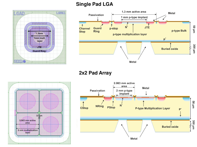
The sensors are thin pixelated n-on-p silicon sensors whose geometry has been optimized for precision time measurements. They are based on the LGAD design [8, 9] developed by the Centro Nacional de Microelectronica (CNM) Barcelona within a RD50 Common Project222http://rd50.web.cern.ch/rd50/ (Run 9088). LGADs are based on implanting a few micrometer thick highly doped p-type layer between the high resistivity p-type bulk and the n+ implant, which acts as a high-field charge multiplication layer providing moderate gain of about 5–70. The devices studied here are produced on 4" silicon-on-insulator (SOI) wafers with nominally 50 thickness and 12 kcm resistivity on a 300 thick support wafer and 1 buried oxide. Boron is used as dopant for the p-type multiplication layer. Due to the diffusion of the highly doped n+ and p+ implants at the front and back side, respectively, the active thickness is reduced to about 45 , which is consistent with capacitance measurements. The back-side contact is done through wet-etched deep access holes through the insulator. The wafers contain a variety of pad structures, such as single-pad diodes and segmented arrays of pad diodes with various dimensions. This test uses single pads of overall active area of 1.31.3 mm2 (called LGA) and 22 arrays of pads with 2.0632.063 mm2 or 3.0633.063 mm2 active area each. It should be noted that the region with charge multiplication is slightly less, namely 1.01.0 mm2 for the LGA single pads and 2.0002.000 mm2 or 3.0003.000 mm2 for each pad of the 22 arrays. That means there is an expected region of 63 in between the multiplication layers of adjacent pads in the arrays. Figure 1 shows a top and a side view sketch of an LGA and a 22 mm2 array. The single pads contain a circular opening in the top metallisation for light injection tests, whereas the array pads are fully metallised. The single pad devices are surrounded by a deep n+-implant ("NRing" or Junction Termination Extension, JTE) that protects all sides of the pad from too high fields and hence early breakdown, whereas for the arrays it surrounds only the whole structure, not each pad. Three sets of wafers were produced, identical in the mask design but with a different multiplication layer implantation dose to optimize the gain: cm-2 (low), cm-2 (medium) and cm-2 (high).
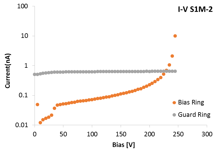
Capacitance-voltage (C-V) and current-voltage (I-V) measurements were performed in the laboratory. The C-V measurements were done with a grounded guard ring and resulted in a depletion voltage below 50 V. The detector capacitance was measured to be C = 3.9 pF for the LGA devices, from which the active thickness of the LGAD, , was derived to be using the relationship , where is the vacuum absolute permittivity, the silicon relative permittivity, and is the active area. The I-V measurements of the LGAD revealed a bulk leakage current of the order of 0.1 nA with a constant guard ring current of about 1 nA before the breakdown voltage (see Fig. 2). The breakdown voltage increases with decreasing multiplication layer dose. For LGA single pad diodes about 80, 250 and 300 V were found for high, medium and low dose, respectively. The breakdown voltage for arrays was found to be reduced (about 200 V for medium dose) due to the absence of a JTE around each pad as explained above.
2.2 Read-out boards
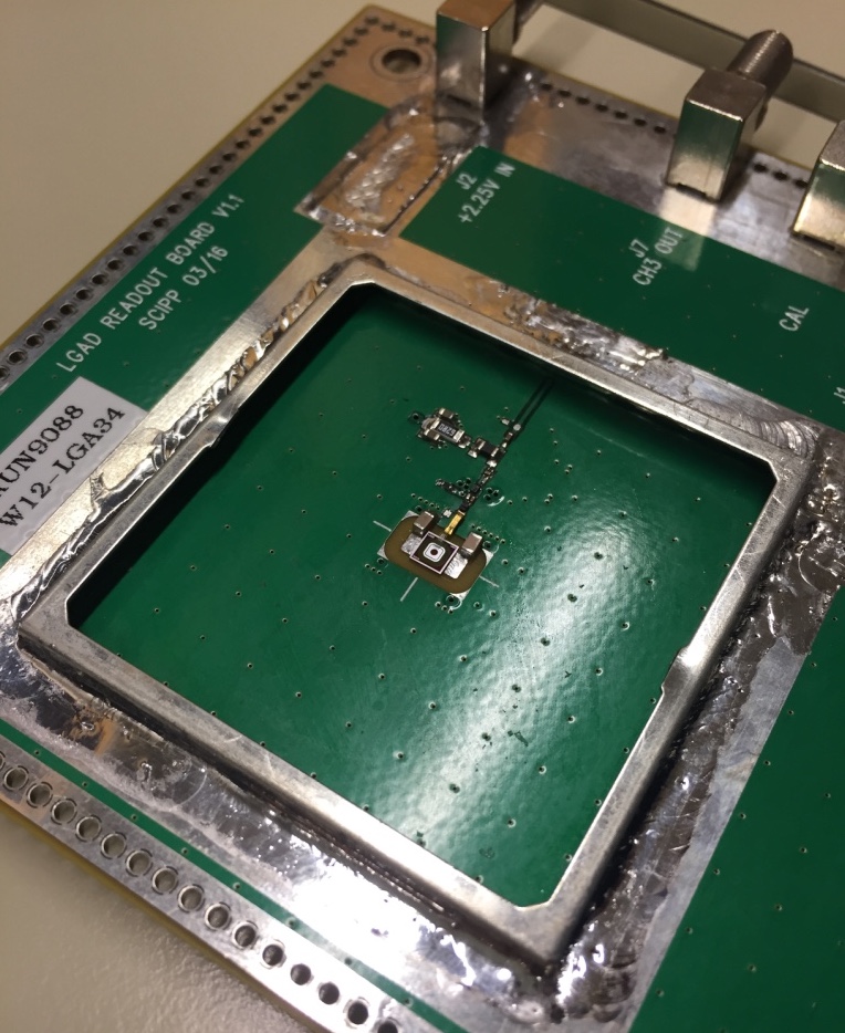
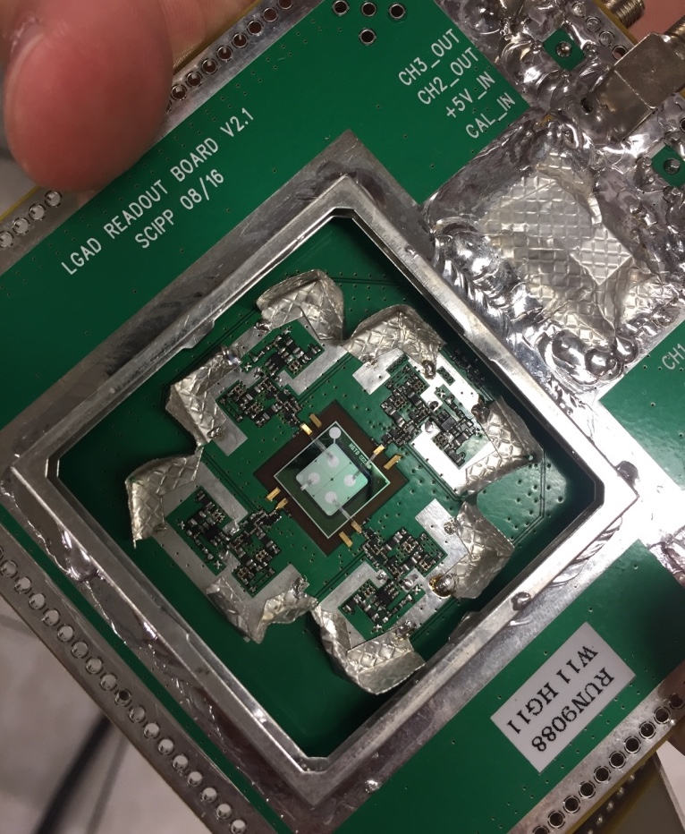
For charge collection studies in the laboratory and the beam test measurements, the LGADs are mounted on 1010 cm2 read-out boards. Three different versions were used: one for single pads (#1), and two different versions of 4-channel boards for the 22 arrays (#2 and #3). They are displayed in Figure 3.
Read-out board versions #1 and #2 were developed at the University of California Santa Cruz (UCSC) [3]. Sensors are attached to the boards using double sided conductive tape while the amplifier input is coupled to the front side metallization layer via multiple wire bonds to minimize inductance. A 1 M resistor attached between input and ground serves for detector biasing, followed by a pair of low forward-resistance silicon pin diodes. The latter, with a 50 V breakdown at 5 , functions as a protection for the amplifier input. The two board versions differ in the number of implemented amplification stages. In version #1, the on-board amplifier includes only the single stage, whose design is described hereafter, followed by a commercial external voltage amplifier333https://ww2.minicircuits.com/pdfs/GALI-52+.pdf with a gain of about 10 and a bandwidth of 2 GHz. Board version #2 incorporates three discrete amplification stages with a voltage divider between the second and the third, resulting in a total gain of about 200 at a bandwidth of 1.6 GHz. The first stage, common to both board versions, is based on a single transistor common emitter design and acts as an inverting trans-impedance amplifier. Simplified schematics are shown in Figure 4(a). Amplification is performed by an AC coupled silicon-germanium bipolar transistor with a bandwidth of 75 GHz. At a bandwidth of 1.9 GHz a gain of 29 dB is expected, with an integrated output noise of 260 . The feedback loop is designed for timing with small capacitance sensors inducing typical rise times of the order of 800 ps, with a feedback resistor of 470 . The overall trans-impedance of the two board designs within a 1.6 GHz bandwidth and terminated into 50 is listed in Table 1. These values include, in the case of board version #1, also the external amplifier and are affected by an overall scale uncertainty of 10%. Care is taken to provide complete hermetic shielding on both sides of the board up to a bandwidth of 3 GHz, with RC filtering in both the high and low voltage input lines. The PCB design has been optimized to minimize parasitics and reduce inductance on the signal return path using at least 6 decoupling high voltage capacitors, 0201 size surface mount components and ground buried signal and power lines.
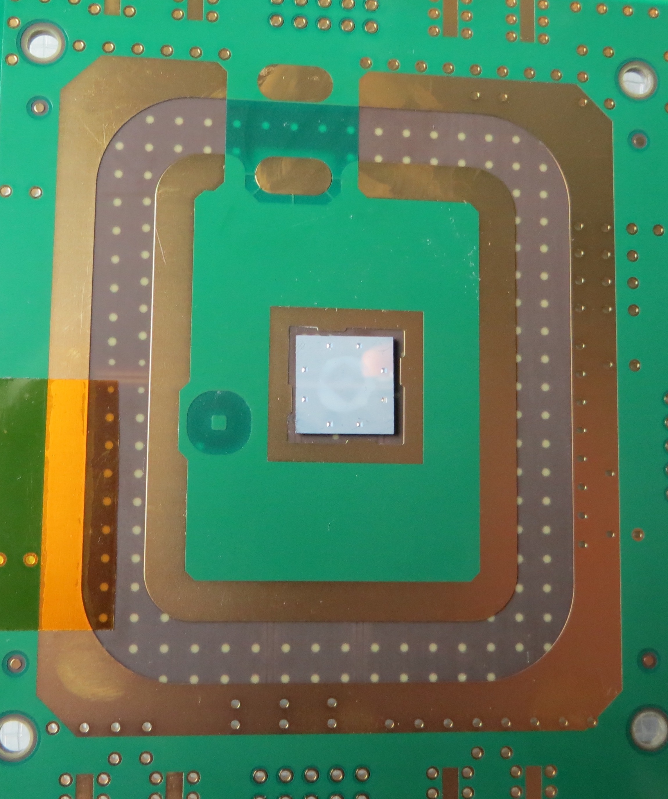
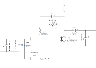
Read-out board version #3 for 33 mm2 sensor arrays was developed by LAL/IN2P3. Simplified schematics of its amplifier are shown in Figure 4(b). The amplifier consists of a regulated cascode trans-impedance amplifier (Q2, Q3), an emitter follower (Q1) and a voltage post-amplifier (THS4303 operational amplifier with a fixed gain of 10, 1.8 GHz bandwidth). The front-end is realized with discrete components. The regulated cascode configuration is expected to achieve higher bandwidth with a relatively high-capacity detector (tens of pF) than would otherwise be possible with a larger input-impedance trans-impedance amplifier. The trans-impedance gain of the first stage is determined by RG=3 k. The overall trans-impedance gain of the full amplifier, properly terminated into 50 , is expected to be about 12.5 k, within a 1 GHz bandwidth. The circuit in its four-channel version was realized on a standard PCB (glass epoxy laminate) with the additional complication of providing adequate clearance for high voltage biasing of the LGAD sensor. Precautions are taken to minimize parasitics: ground plane openings below the sensitive nodes; 0.4 mm wide, short traces; usage of 0201-size based series resistors (to minimize inductance). However the initial version, with a higher Q3 bias current, was prone to oscillation at around 4 GHz at the inner Q2-Q3 loop. The gain of the inner loop was therefore decreased; the actual biasing resistor values are those shown in the present schematics. A more detailed analysis indicates the instability is likely caused by parasitic inductance in that loop (especially in the Q2 base connection). The LGAD sensor is connected to the PCB using a conductive glue: a technique developed by the CALICE collaboration444https://twiki.cern.ch/twiki/bin/view/CALICE/WebHome and only applicable to large pads ( 33 mm2). A robot deposits some dots of glue near the centre of each pad with an optical position control. The amount of glue (150 thickness) is calibrated to ensure a low-resistivity contact between the sensor pads and the PCB pads while avoiding any leakage to neighbouring pads. The positioning and alignment of the sensors is crucial; the sensors should be placed within 100 of the lateral dimension of the PCB pads. Figure 3(c) shows the PCB board with the glued sensor at the center.

2.3 Cherenkov counters
Fast Cherenkov counters with time resolutions similar to or better than the sensors [10, 11] are used as timing references. They consist of Cherenkov-light emitting quartz bars of 10 mm length along the beam, coupled to Silicon Photomultipliers (SiPM) of matching area. Details are given in Ref. [3]. To match the active area of the tested LGAD, one counter, referred to in the following as SiPM1, has an area of 33 mm2 transverse to the beam, and the other, referred to in the following as SiPM2, has an area of 66 mm2 transverse to the beam.
2.4 Devices under test
A complete list of the devices studied in this beam test is presented in Table 1, including the sensor name, information on the pad multiplicity (single pads or arrays), size and pad capacitance, as well as on the implant dose of the p+ multiplication layer and the total trans-impedance of the read-out board and external amplifier combination. Also the maximum voltage applied to each device is included, which was determined by a leakage current level of about 5 , beyond which operation was not considered safe anymore due to reaching the breakdown regime.
| Device | Sensor | Pad | Pad Size | C | p+ Dose | Read-out | Trans- | Max. |
|---|---|---|---|---|---|---|---|---|
| Name | Mult. | [mm2] | [pF] | [ cm-2] | board v. | Imped. [] | V [V] | |
| S1M-1 | W5 LGA31 | 1 | 1.31.3 | 3.9 | 1.9 | #1 | 17540 | 240 |
| S1M-2 | W5 LGA33 | 1 | 1.31.3 | 3.9 | 1.9 | #1 | 4700 | 240 |
| S1H | W12 LGA34 | 1 | 1.31.3 | 3.9 | 2.0 | #1 | 4700 | 85 |
| A2M | W7 HG22 | 22 | 22 | 11 | 1.9 | #2 | 10700 | 180 |
| A3M | W8 HG11 | 22 | 33 | 22 | 1.9 | #3 | 12500 | 200 |
| Nomenclature for Device Name and Read-out Board #: | |||
| Board | Pad size [mm] | p+ Dose | # |
| “S” = single | “1” = 1.3 | “L” = low | for identical |
| “A” = 2x2 array | “2” = 2 | “M” = medium | boards |
| “3” = 3 | “H” = high | ||
3 Beam test setup
The results presented in the following are obtained from data collected in 2016 during a two-week beam test in October/November, at the H6B beam line of the CERN-SPS North Area with 120 GeV pions. Two data-taking modes can be distinguished: stand-alone and integrated into a beam telescope.
In stand-alone mode the pulses of up to 3 LGAD sensors were read out simultaneously by an Agilent Infiniium DSA91204A oscilloscope with 40 GSample/s sampling rate and a bandwidth of 12 GHz. Apart from single test runs, the bandwidth was mostly reduced to 2 GHz for data taking, in order to reduce high frequency noise contributions. The vertical scale of the oscilloscope was adjusted for each run to only saturate the pulse height in a few percent of the events, while minimizing the quantification noise contribution from the oscilloscope. The Cherenkov counter (see Section 2.3) with a time resolution expected to be significantly lower than that of the sensors under test was also included in the data taking, connected to the fourth and last available channel of the oscilloscope. Since the quartz bar had a much larger surface than the LGAD sensors, its use as a trigger would have made the geometrical efficiency very low. Therefore one of the sensors was used as a trigger, while voltage scans were performed on a different one. A custom-made support structure provided mechanical stability and the correct alignment of the sensors and SiPMs. The setup was mounted on a base plate connected to remotely controllable stage motors moving in the horizontal and vertical directions perpendicular to the beam direction with micrometer precision. This allowed for a precise positioning of the sensor at the centre of the beam. To provide light-tightness for the operation of the SiPM, the base plate was covered with a styrofoam box.
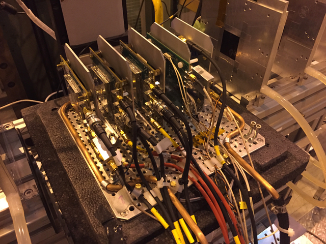
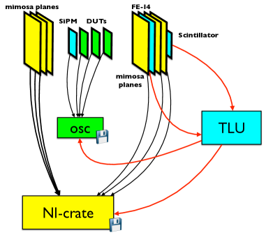
At a later stage a EUDET-type beam telescope based on MIMOSA pixel planes with a track position precision of few micrometers [12] was also included in the data taking, allowing for a position-dependent measurement. A picture and a schematic drawing of the setup are shown in Figure 5(b). The pulses of up to 8 sensors were read out by one or two oscilloscopes with 10 or 40 GSample/s and 2 or 3 GHz bandwidth. In the configurations with more than 4 channels, additionally to the same oscilloscope used in stand-alone mode, an Agilent Infiniium DSO9254A oscilloscope with a sampling rate of 20 GSample/s for up to 2 channels (10 GSample/s otherwise) and a bandwidth of 2.5 GHz was used. Both oscilloscopes were set to use the same bandwidth and sampling rate. Whenever the beam telescope was included in the data acquisition, the trigger was provided by the coincidence of signals on a scintillator and a special 3D FE-I4 plane. This plane, consisting of a 3D CNM Silicon sensor connected to the FE-I4 read-out chip as also used in the ATLAS IBL [13], is a pixel detector with pixel size of 50 and 250 in the (horizontal) and (vertical) direction, respectively, and 25 ns clock. It served two purposes. Firstly, it provided a so-called hitOr trigger that fires when at least one of the pixels selected in a user-defined mask has a hit. Hence, it was used as a region-of-interest (ROI) trigger to only accept tracks traversing the small area of the LGAD sensors. Secondly, with its 25 ns time binning of the hits it has a very short integration time, compared to the telescope planes that integrate hits over 112.5 and hence usually provide multiple tracks within this period at the typical SPS particle rates. Hence, by matching the mostly unique signal of the FE-I4 plane to one of the several tracks provided by the telescope, the track that fired the trigger can be selected. The trigger signals were combined in the Trigger Logic Unit (TLU) [12], whose output was used by the telescope and connected to the oscilloscope, thus ensuring a perfect correspondence between the events recorded by the oscilloscope(s) and by the telescope. The two data acquisition chains were separate and the information from both systems were combined offline. The data from the LGAD sensors and Cherenkov counter were collected by the oscilloscope(s) described above, while the beam telescope and FE-I4 data were saved in a National Instrument (NI) PXIe crate [12]. The synchronicity of the two data streams was constantly monitored and never failed as long as the SPS provided a regular spill structure. Either the same support used for stand-alone data-taking or single metal frames (see Fig. 5(a)) were used to position the sensors perpendicular to the beam. The movable table, on which the sensors and SiPMs were positioned, was used to align the setup with the beam telescope and FE-I4 plane, while the whole system was aligned to the centre of the beam with another set of remotely controllable stage motors. The styrofoam box covering the devices under test was used both for light-tightness and to keep a stable temperature of about 25∘C with a water cooling system. A nitrogen outlet available in the area was inserted in the box to avoid humidity condensation that would damage the sensors.
4 Data reconstruction and analysis methods
4.1 Oscilloscope data reconstruction
For each event and for each channel, at least 2000 samples were registered spaced every 25 ps. The first step in the oscilloscope data reconstruction is to measure the pedestal and the noise computed as the mean and standard deviation of the measured voltage, respectively, using the first 240 samples where no signal contribution is expected. The pedestal varies from 1 to 5 mV depending on the run conditions and oscilloscope settings and is subtracted from the measured pulses event-by-event. The noise was found to be independent of the bias voltage, as expected, since the leakage current of the sensor is negligible with respect to the electronic noise. The run-by-run variations (up to 20%) are attributed to different settings of the oscilloscope. Table 2 shows the average noise measured for each sensor. For arrays the noise correlation between pads was also measured and found to be negligible for A2M and of the order of 30% for A3M, due to the different read-out board versions.
| Sensor | Noise (mV) | |||
|---|---|---|---|---|
| Single pad sensors | ||||
| S1M-1 | 2.6 | |||
| S1M-2 | 2.2 | |||
| S1H | 2.2 | |||
| Arrays - pad number | ||||
| 1 | 2 | 3 | 4 | |
| A2M | 4.6 | 5.4 | 4.9 | 4.7 |
| A3M | 2.3 | 2.4 | 2.7 | 2.3 |
The maximum of the pulse amplitude is estimated after pedestal subtraction with a second-degree polynomial fit around the sample with the highest amplitude in a 400 ps window. The collected charge is defined as the integral of the signal voltage after pedestal subtraction divided by the trans-impedance (see Table 1). The integral is computed numerically in a window centered around the time where the pulse is maximal and wide enough to fully contain the pulse. The gain is then obtained by dividing the collected charge by the expected charge from a MIP in a silicon sensor without gain (). For a 45 thick sensor, the value of is 0.46 fC [14]. The gain has an estimated systematic error of 20% due to the uncertainty on the trans-impedance.
Selections on the maximum amplitude are applied to reject noisy events (lower cut) and to reject saturated pulses that might be caused by the oscilloscope or the read-out electronics (upper cut). These selections are derived separately for each channel and each run.
The optimal time resolution is expected to be reached with sophisticated time reconstruction techniques using the full information of the pulse shape (e.g. digital filtering). However, since these techniques require a too large data bandwidth and cannot be used for the HGTD read-out, only three time reconstruction algorithms using discriminators are investigated in this paper. The first and simplest one is the Constant Threshold Discriminator (CTD) method where the time of arrival is defined as the time where the signal crosses a constant threshold. In order to be above the noise level, a value of 20 mV has been chosen. The time of arrival is determined from a linear interpolation between the samples just above and below the threshold. The drawback of the CTD method is that it suffers from time walk effects, which can be corrected if the signal amplitude is known. Quite often the amplitude is not directly measured and the Time-Over-Threshold (TOT) information, correlated with the amplitude, is provided by the discriminator output. The Constant Fraction Discriminator (CFD) method minimises the time walk effect by defining the time of arrival as the time where the signal crosses a constant fraction () of the maximum amplitude. However, since the threshold is crossed before the maximum amplitude is reached, this method cannot be implemented in the read-out electronics. A third method reconstructs a time of arrival that is independent of the amplitude of the signal: the Zero-Crossing Discriminator (ZCD). A copy of the signal is delayed by and attenuated by a factor . The zero-crossing time of the difference of the original signal and the attenuated copy is by construction independent of the signal amplitude under the assumption that the pulse shape remains identical. The CTD method with TOT-based time walk correction and the ZCD555One significant difference between the ZCD method implemented in this paper and the one under investigation for the HGTD front-end electronics is the use of an additional arming discriminator necessary to gate the zero-crossing discriminator output and avoid triggers induced by the noise which is not mandatory for an offline analysis. methods are the two methods under investigation for the HGTD front-end electronics.
The time of the SiPM is always reconstructed using the CFD method with . The optimization of the CFD and ZCD algorithms for LGADs is presented in Section 5.4.1. The default time reconstruction algorithm for LGAD sensors used in the following is the ZCD method.
The time resolution can be extracted from the width of the time differences computed from the LGADs and the SiPMs. Assuming that N devices with time resolutions are used, there are N(N-1)/2 possible combinations. Assuming that the time resolutions of the devices are independent, for each combination, one has:
| (4.1) |
where is the width of the time difference distribution between device and and it is estimated as the width of a Gaussian function fitted iteratively on a range [-3,3]. Therefore, one has N unknowns and N(N-1)/2 constraints. For N2, the system is under-constrained and no solution can be found without further assumptions. For N3, the number of constraints equals the number of unknowns. In this case, the system of equations is linear considering the square of the time resolution as the unknown and it can be solved analytically. For N3, the system is over-constrained and in order to fully use the available information, the time resolution can be extracted using a minimization technique:
| (4.2) |
where is the uncertainty on . The time resolutions are extracted using the method for runs where 4 measurements are available (3 LGADs and 1 SiPM). The time resolutions of SiPM1 and SiPM2 are found to be (10.90.8) ps and (35.31.9) ps, respectively, with up to 10% variation due to varying running conditions (e.g. bias voltage settings). The time resolution measurements of the LGADs are presented in Section 5.4.4.
4.2 Telescope data reconstruction and performance
The beam telescope consists of 6 MIMOSA planes. Planes 0, 1 and 2 are located upstream of the DUTs and planes 3, 4 and 5 are located downstream of the DUTs. The FE-I4 plane used for triggering is located between the MIMOSA planes 3 and 4. The setup is shown in Figure 5(b). The positions of the telescope, FE-I4 and DUT planes are known with a precision of 1 mm in the direction along the beam line. The dimension of the MIMOSA planes is 10.621.2 mm2 in the and directions with a pixel size of 18.518.5 2. In order to reconstruct the hit position on each DUT plane, tracks are reconstructed using the information from all the 6 planes (or only 4 of them in a small part of the dataset where 2 of the planes had readout problems).
The first step in the reconstruction of tracks is the removal of the “hot” pixels from the MIMOSA planes. Clusters are then built from the remaining hits in each plane. Only clusters with a maximum of 6 hits are used for tracking. In the FE-I4 plane, a cluster has a maximum of 2 neighbouring hits. The cluster coordinates are the mean values of the hit coordinates in and . In order to select events with only one particle traversing the DUTs, only events with exactly 1 such cluster in the FE-I4 plane are considered (about 94 % of the total number of events).
The MIMOSA planes are aligned by iteratively shifting the planes coordinates in and with respect to a reference plane, in order to minimize the difference between the reconstructed track position at the MIMOSA plane and the measured hit position in the same plane.
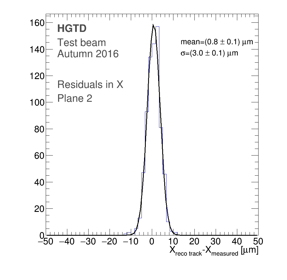
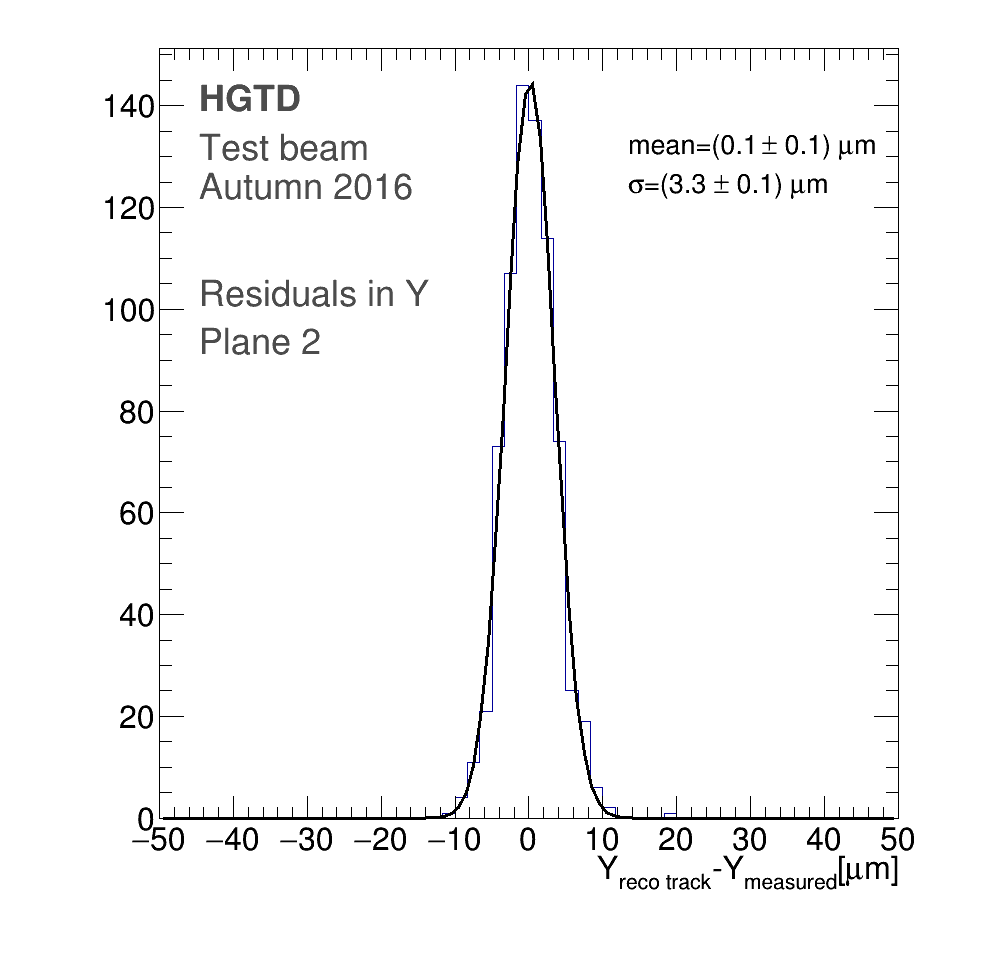
Once the planes are aligned, the track fitting procedure is applied: knowing the -position of the MIMOSA planes along the beam axis and the (,) positions of the hits in these planes, 3D-tracks are built from the six planes of the telescope starting with the planes closest to the FE-I4. The reconstructed tracks must coincide with a hit in the FE-I4 plane and only events with a single reconstructed track through the six MIMOSA planes are considered. The residuals, defined as the difference between the track position in a MIMOSA plane and the hit used to build the track, are shown in Figure 6 for plane 2 (the closest to the DUT’s). The precision on the position of the extrapolated reconstructed track in the DUT planes is about 3 in the and directions.
The tracking efficiency, defined as the number of events with one reconstructed track divided by the total number of events with one cluster in the FE-I4 is about 77% mostly due to the exclusion of inefficient and noisy regions in the MIMOSA planes. Furthermore only straight tracks were considered in order to have a precise interpolation to the DUT.
5 Results
5.1 Pulse properties
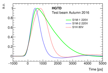
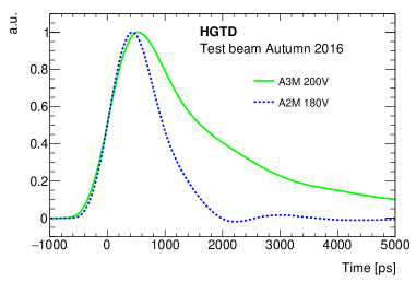
The performance of a LGAD sensor depends strongly on the characteristics of its pulse shape (e.g. charge and rise time). Figure 7 shows the averaged pulse shapes for single pads and arrays normalized to the maximum pulse amplitude. The averaging was performed after synchronising the signals. The pulse shapes are given by the convolution of the intrinsic LGAD waveform with the electronics response functions, therefore they are different for the identical sensors, S1M-1 and S1M-2, read out by boards with different trans-impedance amplifier characteristics. The pulse shapes of S1M-2 at 220 V and S1H at 80 V, differ slightly, in spite of the sensors being connected to the same amplifier type, due to the significantly lower bias voltage and hence drift velocity for S1H, which leads to longer rise time and larger pulse width.
5.1.1 Amplitude and charge
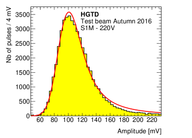
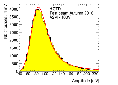
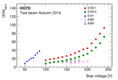
Examples of the maximum pulse amplitude distributions are shown in Figure 8. In order to estimate the most probable value, the distributions are fitted with a Landau function convoluted with a Gaussian function. These most probable values are used to compute the signal-to-noise ratio (S/N), that is shown in Figure 9(a) as a function of the bias voltage. As expected, S/N increases with increasing bias voltage. Due to their larger capacitance, arrays have lower signal-to-noise ratios compared to single pads. Larger signal-to-noise ratio is measured for S1M-1 compared to S1M-2 due to the larger trans-impedance of its read-out board. The best signal-to-noise ratio is reached for S1M-1 at 240V with a value of 94.
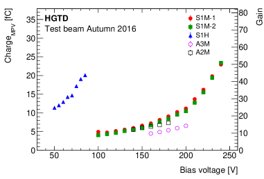
The charge distributions are fitted with the same function used for the amplitude in order to extract the most probable value. Figure 9(b) shows the most probable value of the charge and the gain as a function of the bias voltage. Sensors with medium doping need higher bias voltage to reach the same gain as sensors with high doping. For instance, a gain of 30 is reached at 210 V for sensors with medium doping compared to 65 V for sensors with high doping. As expected, the gain is similar for S1M-1 and S1M-2 and the highest gain (50) is obtained for the largest bias voltage. The gain is found to be smaller for the arrays with medium doping and the highest value (16) is obtained for A2M. Sensors of the same thickness and with the same doping are expected, within uncertainties, to have the same gain for a given bias voltage. However, the sensor A3M equipped with a quite different preamplifier shows a smaller gain than expected. The most probable cause is the trans-impedance being incorrectly determined for the used bandwidth.
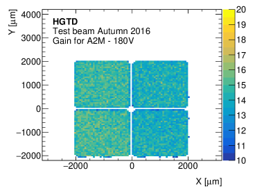
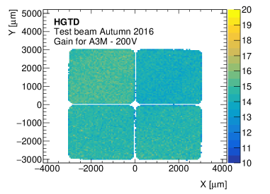
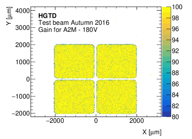
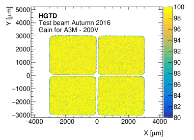
The gain is not only measured inclusively, but also as a function of the position in the pads by combining the beam telescope track position at the DUT coordinate with the signal on the LGAD detector (see Figures 10, 11). The gain is derived for each DUT position from the charge distribution with the same procedure used for the inclusive measurement. The circular structure in the central part of the S1M-1 sensor has a slightly lower gain than the external part of the DUT. This shape corresponds to the opening in the metal layer used for laser testing, where a small potential drop is expected.

5.1.2 Rise time and noise jitter
The rise time, computed as the elapsed time from 10% to 90% of the pulse amplitude, is a critical parameter of a timing device. For a given signal-to-noise ratio, the faster the rise time is, the better the time resolution is. The measured pulse rise times as a function of the gain are shown in Figure 12(a) for single pads and arrays. The rise time decreases when the bias voltage is increased, due to the faster drift mobility. Sensors with higher doping have larger rise time for a given gain due to the lower operating bias voltage. For the sensors with medium doping, a larger rise time is measured for S1M-1 compared to S1M-2. The fastest rise time measured with S1M-2 at large gain is 420 ps.
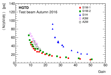
One of the contributions to the LGAD time resolution is the electronic jitter defined as where is the electronic noise and is the derivative of the pulse when the signal crosses the threshold. The measured jitter values as a function of the gain are shown in Figure 12(b). As expected, the jitter decreases with increasing gain. The high doping sensors exhibit a larger jitter for the same gain value mostly correlated to the larger rise time. The smallest jitter (8 ps) is obtained for single pads with medium doping at the largest gain. At a gain of 14 (the largest value obtainable for A3M), the jitter decreases from 45 ps at large capacitance value (22 pF for A3M) to 26 ps for the smaller ones (3.9 pF for S1).
It should be noted that the jitter depends on the time reconstruction method. For the ZCD method, 666For the ZCD pulse, the noise is given by where is the noise autocorrelation function. For all sensors, is smaller than 0.1 except for S1M-1 which has . and should be computed for the ZCD pulse, i.e. the difference of the original pulse and the delayed and attenuated copy. The jitter computed for the ZCD method is found to agree within a few percent with the jitter computed for the CFD method with few exceptions. For S1M-2, the ZCD jitter is found to be about 20% larger than the CFD jitter at high gain and for A2M the ZCD jitter is found to be about 7% smaller than the CFD jitter.
5.2 Efficiency
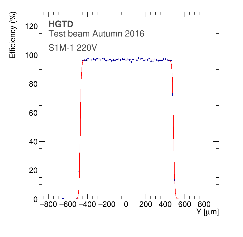
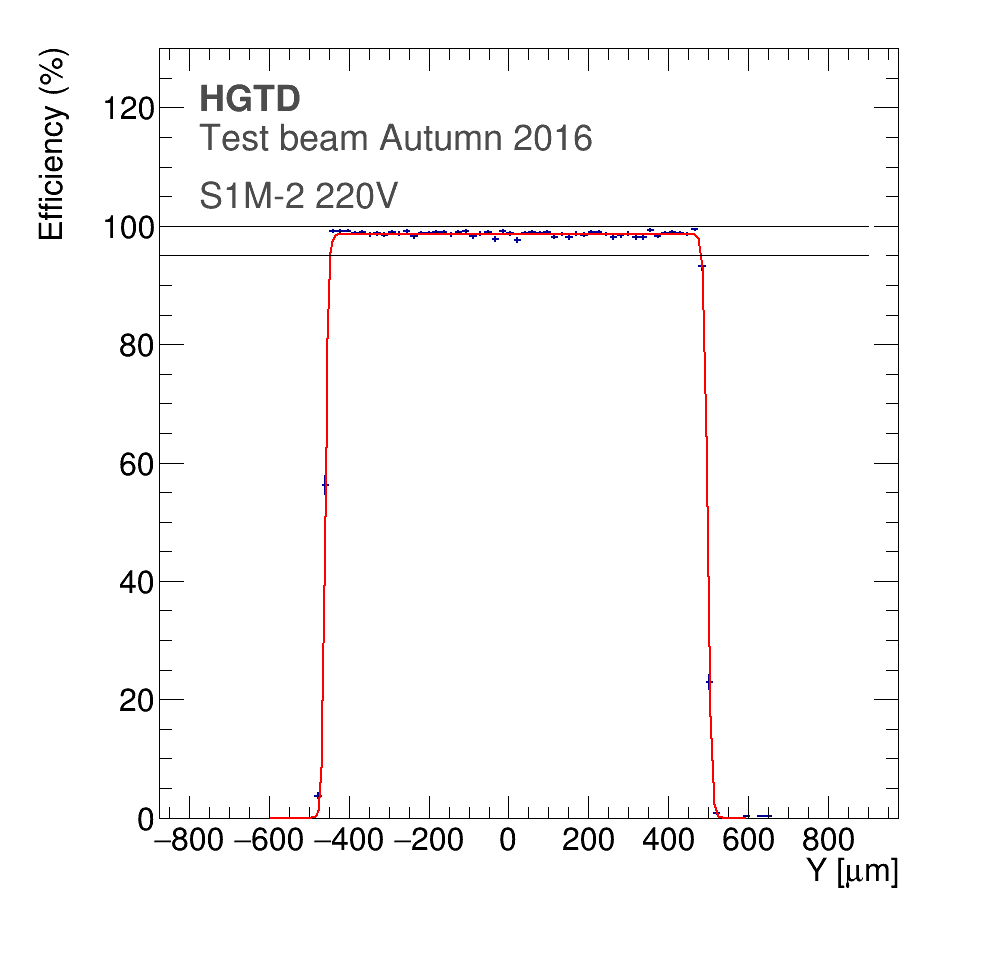
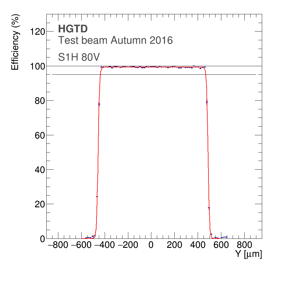
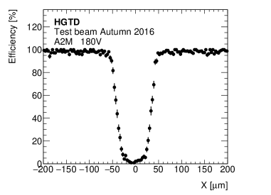
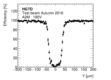
The efficiency at a given position in the pad is defined as the number of hits that induce a sensor response (with amplitude above threshold) divided by the total number of reconstructed tracks crossing the DUT at that position. The amplitude threshold, given in Table 3, is different for each sensor and lies around the minimum between the noise and the signal peaks. The bin size is chosen in order to have a statistical uncertainty in each bin of about 2%. The measured 2D distribution for one single-pad sensor as well as the projections in the direction are shown in Figure 13. These projections are fitted with sigmoid functions. Figure 14 shows the corresponding 2D efficiency distribution for the arrays, while in Figure 15 an example of projections along the and axes can be seen. In the central region of the sensors, the mean values of the plateau efficiency and its dispersions (defined as the RMS of the efficiency distribution on the plateau) are summarised in Table 3. The same table shows also the size of regions where the efficiency is larger than 99.9% or 50% of the plateau efficiency. For the arrays, the width of the inter-pad region for each sensor, defined as the region with efficiency below 50%, is estimated to be (765) , slightly larger than the expected width of 63 . The width estimate is performed by parametrising the edges with Gaussian functions and determining the 50% efficiency point based on the fit parameters and their uncertainties.
| Sensor | Threshold amplitude | Efficiency | Dispersion | Size of the plateau () | |
|---|---|---|---|---|---|
| for the signal | on the plateau | at 99.9% | at 50% | ||
| S1M-1 | 60 mV | % | 0.7% | 876 | 960 |
| S1M-2 | 40 mV | % | 0.4% | 898 | 958 |
| S1H | 30 mV | % | 0.2% | 859 | 945 |
| A2M | 40 mV | % | 1.1% | 1920 | 1995 |
| A3M | 25 mV | % | 1.0% | 2930 | 3006 |

5.3 Crosstalk hit probability
Events with signal above a certain threshold on more than one pad were studied independently to estimate detector induced crosstalk hit probability in arrays. The corresponding rate was defined as the ratio of coincidences between two neighbouring pads over the sum of events in each individual pad, reduced by the number of coincidences. The final number is estimated according to Eq. 5.1:
| (5.1) |
where the indices and denote the corresponding pads. In this section a hit is defined as any event with a signal amplitude over 30 mV in any of the examined pads. The crosstalk ratio is estimated to be and for the A2M and A3M DUTs, respectively. The common threshold was set at 30 mV threshold to be well within the gap between the noise and the signal amplitude peaks in each pad of both DUTs.
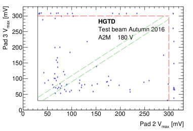
Considering the amplitudes and time differences of the signals, three regions can be identified originating from different sources. All events are required to be in-time, i.e. their maximum amplitude must lie within ns. Double hits can show saturation in either or both pads (“saturation events”), similar amplitudes in both pads (“correlated crosstalk”) due to a particle hitting the interpad region, or different amplitudes (“uncorrelated crosstalk”) . Figure 16(a) shows the amplitudes in the two hit pads with > 30 mV and ns.
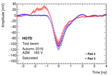
- Saturation events
-
This region refers to events with amplitude close to the highest possible value that can be recorded by the oscilloscope at the chosen settings in one channel, accompanied by a secondary hit in a neighbouring channel with lower amplitude. The channel where the highest amplitude is reached, referred to as the primary channel, results in an increased charge injection within the bulk that distorts the electrical field. This field distortion may propagate to the closest neighbour inducing a secondary signal that will typically be of smaller amplitude but within the same time window as the primary event. Double hit events are considered to belong to this category if the signals have an amplitude of at least 300 mV in at least one of the channels while being within a 2 ns time window of each other. They represent 0.1% and 0.2% of the total number of hits for the A2M and A3M DUTs, respectively, and in the time of arrival vs. amplitude plane, they are mainly positioned around the ns line, while amplitudes of the secondary hit are spread from the lower to the higher extremities of the distribution. The average signal shape in the non-saturated pad of A2M in this kind of events is shown in Figure 16(b).
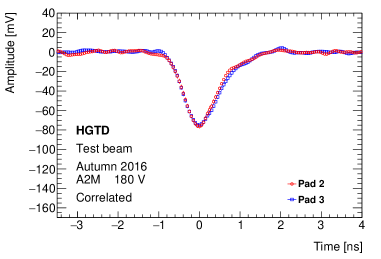
- Correlated crosstalk
-
In the case of an event occurring in the space between pads, a signal is induced in both pads with a ratio of amplitudes directly related to the distance of the hit to each pad border. This type of events is easily identifiable in the special case where the original hit occurred close to the middle of the inter-pad region. Recorded signals will be on time with one another and of similar amplitudes, thus mainly concentrated on the diagonal of the amplitude correlation plot between different channels. As expected, these events represent a very low fraction of the total recorded hits, corresponding to 0.05% and 0.1% for the A2M and A3M DUTs, respectively. For A2M, their amplitude lies mostly around 75 mV as shown by the average pulse in Figure 16(c).
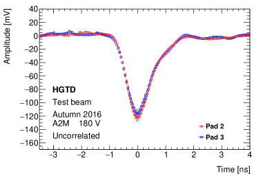
- Uncorrelated crosstalk
-
The case of inter-pad coincidences where signals do not present any clear correlation is included in this category. The timing requirement of ns is still applied, while to exclude correlated coincidences, the amplitudes of the two signals are required to differ by at least 10 mV. Given the relatively large induced signal amplitudes, these events are not expected to originate from any non-gain region of the DUT, such as the periphery or the space between neighbouring pads. They represent approximately half of the observed crosstalk in both the A2M and A3M DUTs, corresponding to a probability of 0.15% and 0.3%, respectively. Figure 16(d) shows their average pulse with an amplitude similar to the saturated events, but with a much smaller spread.
A summary of all calculated crosstalk hit probabilities for the A2M and A3M DUTs is presented in Table 4. The twice as high level of crosstalk in A3M than in A2M is assumed to originate from the different read-out boards.
| Crosstalk hit probability | ||
|---|---|---|
| Category | A2M | A3M |
| Saturated | 0.10% | 0.2% |
| Correlated | 0.05% | 0.1% |
| Uncorrelated | 0.15% | 0.3% |
| Total | 0.30% | 0.6% |
5.4 Time resolution
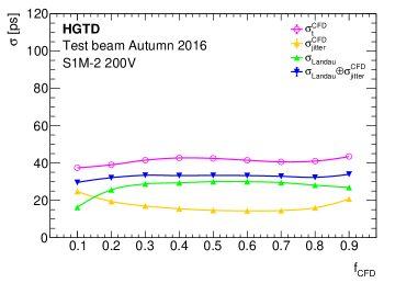
5.4.1 Optimization
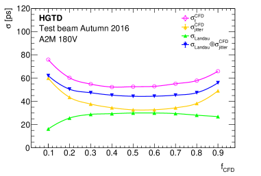
The parameters of the CFD and ZCD algorithms have been chosen in order to optimise time resolution. The constant fraction was scanned in 10% steps from 10% to 90% of the amplitude and the delay was scanned in 200 ps steps from 400 to 2000 ps. Figure 17 shows two examples of two-dimensional resolution map for the ZCD method. For S1M-2 at 200 V, the optimal value of is close to 1 ns, while a slightly lower value is found for A2M at 180 V. Similar results were obtained for other sensors and at different bias voltages. For simplicity, the same value =1 ns is used everywhere, leading to slightly non-optimal time resolution at the level of 5%. For S1M-2 at 200 V, the optimal value of is close to 0.2 while larger values, close to 0.5, are preferred for A2M. The conclusion is similar for the CFD method and the result agrees with the expectation obtained from the quadratic sum of the jitter and the Landau contributions, as shown in Figure 18. The time resolution for single pads at high bias voltage is dominated by the Landau term that prefers low values of the constant fraction [15]. For arrays, the jitter contribution is dominant and this term prefers a larger constant fraction that maximizes . While for arrays the optimal value was found to be close to 0.5 at all bias voltages, for single pads and at high bias voltage (above 150 V for LGADs with medium doping and above 60 V for LGAD with high doping), the optimal value was found to be around 0.2. For lower bias voltage, slightly larger values (0.3) are preferred because the contribution of the jitter increases. While the predictions qualitatively explain the preferred values of the constant fraction, some differences are observed between the measured time resolution and the prediction. The largest difference is observed for A3M with a measured time resolution 40% higher than the prediction.


5.4.2 Method comparison
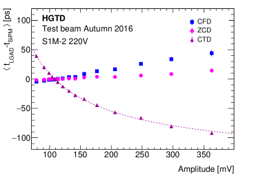
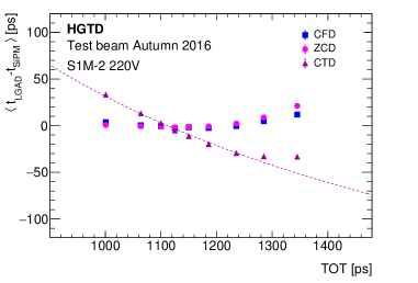
The performance of the different time reconstruction algorithms has been compared for single pads and arrays with medium doping at high bias voltage. The stability of the reconstructed time as a function of the amplitude has been investigated for the various methods. Figure 19(a) shows the mean value of the reconstructed time for S1M-2 at 220 V measured relatively to the SiPM time as a function of the reconstructed amplitude. As expected, a larger time walk is observed for the CTD method with a threshold of 20 mV, with a 50 ps variation in amplitude between 100 and 200 mV (most probable value is 100 mV per MIP as shown in Figure 8). While better behaving, the ZCD and CFD methods still exhibit an increasing time of arrival as a function of the amplitude.
The time resolution has been measured for the three methods. With the CFD method, the resolution is (32.80.1) ps where the uncertainty is only statistical. A better resolution is measured with the ZCD method, (29.30.1) ps, while a significantly larger resolution is measured for CTD (400.1) ps due to the time walk effect. This bias can be minimized by correcting the CTD time as a function of the amplitude. Using the fitted function shown in Figure 19(a), the time resolution has been reduced by about 20% leading to a resolution of (29.90.1) ps. Similar corrections have been tested for the two other methods, leading to improvements smaller than 5%, as expected. If the full pulse shape is not available, the TOT can be used as an estimate of the amplitude. Here a fixed threshold of 20 mV is used to compute this quantity. For S1M-2, and more generally for single pads close to breakdown voltage, distorted pulses are observed leading to high TOT values uncorrelated with the amplitudes. This is due to cases in which the holes in the amplification region start to show multiplication too. Distorted pulses close to the breakdown voltage are rejected using an upper cut on the TOT. This requirement rejects up to 5% of the events at the highest bias voltage. Figure 19(b) shows the mean value of the reconstructed time for S1M-2 as a function of the TOT. A smaller dependence is observed because the correlation factor between the TOT and the amplitude is only 0.60. The time resolution with TOT correction is (31.30.1) ps which is 5% worse than the time resolution with the amplitude correction. Similar analyses were performed for other sensors and at different bias voltages. The results are summarized in Table 5. The best performance is obtained with the ZDC algorithm, chosen as the default algorithm in this paper, but difficult to implement in an ASIC. Currently the CTD method is used in the ASIC with offline correction of the timewalk with the TOT information. For single pad sensors at all bias voltages the time resolution measured with the CTD method with TOT correction is less than 7% worse than with the ZCD method, in some cases even slightly better.
| Time resolution [ps] | ||||||
| CTD | ||||||
| Sensor | voltage | CFD | ZCD | no | amplitude | TOT |
| (V) | correction | correction | correction | |||
| 200 | 38.6 0.1 | 36.9 0.1 | 49.4 0.1 | 34.8 0.1 | 39.3 0.1 | |
| S1M-1 | 220 | 34.2 0.1 | 33.1 0.1 | 38.3 0.1 | 29.4 0.1 | 33.0 0.1 |
| 240 | 27.1 0.1 | 27.4 0.1 | 30.8 0.1 | 25.4 0.1 | 27.9 0.1 | |
| 200 | 38.3 0.1 | 34.7 0.1 | 55.1 0.2 | 36.8 0.2 | 37.0 0.2 | |
| S1M-2 | 220 | 32.8 0.1 | 29.3 0.1 | 40.0 0.1 | 29.9 0.1 | 31.3 0.1 |
| 240 | 27.9 0.1 | 27.8 0.1 | 31.6 0.1 | 25.5 0.1 | 27.5 0.1 | |
| A2M | 140 | 73.9 0.5 | 63.4 0.5 | 102.0 0.7 | 69.5 0.7 | 64.3 0.7 |
| 180 | 51.1 0.3 | 47.0 0.3 | 74.1 0.5 | 51.8 0.5 | 54.4 0.5 | |
5.4.3 Gain dependence
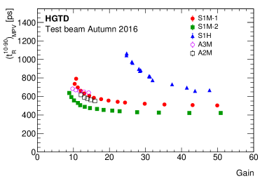
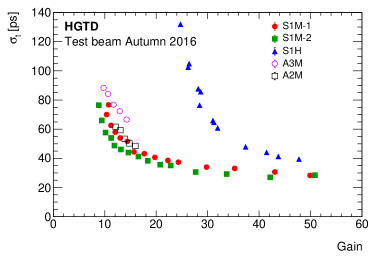
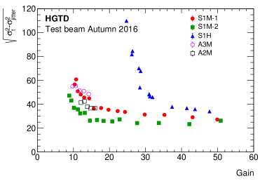
Figure 20(a) shows the time resolution for the ZCD method () as a function of the gain for single pads and arrays. Two approximately universal behaviours are observed for sensors with medium and high doping and, at a given gain, the best performance is obtained for sensors with medium doping. For a gain around 14, the best time resolution is (44.00.5) ps for S1M-2, while a worse resolution is obtained for sensors with larger pad size as expected from Figure 12(b): (53.40.6) ps for A2M and (66.60.4) ps for A3M. In addition to the larger noise, the performance of the arrays is limited by the lowest achievable gain due to the reduced breakdown voltage. The best time resolution (27 ps) is obtained at the largest gain reached by single pad sensors.
The quadratic difference between the measured time resolution and the electronic jitter () is shown in Figure 20(b). Assuming that the time resolution has only two contributions, the Landau fluctuation () and the electronic jitter, this difference should be equal to . As expected from the simulation [16, 17], a plateau is reached at the higher gain where the Landau fluctuations is the dominant contribution to the time resolution. For small gain values the difference is not constant anymore: it increases, showing that additional contributions are present, whose origin has not yet been identified.
5.4.4 Uniformity
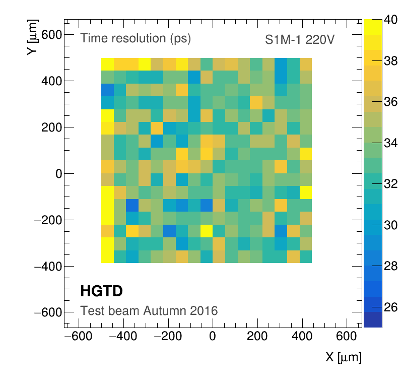
For single pads, the time resolution is calculated by measuring the width of the time difference between a given sensor and the fast SiPM for which the time resolution was measured with the test beam data to be 10.9 ps. The distribution of the time resolution as a function of the position on the pad is shown as a two-dimensional map in Figure 21 for S1M-1 at 220 V. The bin size is (55.5 )2 and only bins with at least 100 events are considered. The uncertainty is below 2 ps in each bin and the time resolution is uniform within a few picoseconds over the DUT777For this voltage the time resolution variation as a function of the gain is small, explaining why the circular shape is not observed.
A position dependent measurement of the time resolution was not possible for arrays due to the poor alignment of the sensors that only allowed for a small overlap region that could be traversed by the same particles.
6 Conclusion
Several measurements on single LGAD sensors with a surface of 1.31.3 mm2 and arrays with 22 pads with a surface of 22 mm2 or 33 mm2 each have been obtained from data collected during a beam test campaign in autumn 2016 with a pion beam of 120 GeV energy at the CERN SPS. All sensors had the same thickness of 50 , but different implantation doses in the multiplication layer. Gain, efficiency and time resolution have been measured inclusively and as a function of the position of the particle inside the sensor by using a beam telescope with a position resolution of few micrometers. The efficiency is uniform within 1% over the surface of each pad and the time resolution within 2 ps. Furthermore, the fraction of events with hits above threshold in two neighbouring pads of the arrays was found to be well below 1%. Based on the efficiency measurement, the size of the active area was estimated and found to be compatible with the expectation from the sensor production. The sensors with a medium doping dose show better performance than the ones with a high dose and the sensors with a small surface have, as expected, a better time resolution than the larger ones. The tested non-irradiated sensors with a surface of 1.31.3 mm2 fulfil the requirements of a time resolution of about 30 ps for a gain of 35 (down to 27 ps at a gain of 50) and are considered good candidates to be used for the ATLAS High Granularity Timing Detector. The time resolution was measured with different algorithms yielding consistent results. In particular, the suitable ones for implementation in the read-out electronics have similar performance as the optimal one that can only be used offline.
Acknowledgements
The authors gratefully acknowledge CERN and the SPS staff for successfully operating the North Experimental Area and for continuous supports to the users. We acknowledge the expert contributions of the SCIPP technical staff. Part of this work has been performed within the framework of the CERN RD50 Collaboration.
The work was supported by: the United States Department of Energy, grant DE-FG02-04ER41286; the MINECO, Spanish Government, under grants FPA2013-48308-C2-1-P, FPA2014-55295-C3-2-R, FPA2015-69260-C3-2-R, FPA2015-69260-C3-3-R (co-financed with the European Union’s FEDER funds) and SEV-2012-0234 (Severo Ochoa excellence programme), as well as under the Juan de la Cierva programme; the Spanish ICTS Network MICRONANOFABS partially supported by MINECO; the Catalan Government (AGAUR): Grups de Recerca Consolidats (SGR 2014 1177); the European Union’s Horizon 2020 Research and Innovation programme under Grant Agreement no. 654168 (AIDA-2020); the Cluster of Excellence Precision Physics, Fundamental Interactions and Structure of Matter (PRISMA – EXC 1098) of the German Research Foundation.
References
- [1] ATLAS Collaboration, The ATLAS Experiment at the CERN Large Hadron Collider, JINST 3 (2008) S08003.
- [2] H. F. W. Sadrozinski et al., Ultra-fast silicon detectors (UFSD), Nucl. Instrum. Meth. A831 (2016) 18–23.
- [3] N. Cartiglia et al., Beam test results of a 16 ps timing system based on ultra-fast silicon detectors, Nucl. Instrum. Meth. A850 (2017) 83–88, [1608.08681].
- [4] J. Lange et al., Gain and time resolution of 45 m thin Low Gain Avalanche Detectors before and after irradiation up to a fluence of neq/cm2, JINST 12 (2017) P05003, [1703.09004].
- [5] Z. Galloway et al., Properties of HPK UFSD after neutron irradiation up to 6e15 n/cm2, 1707.04961.
- [6] G. Kramberger et al., Radiation Hardness of Thin Low Gain Avalanche Detectors, 1711.06003.
- [7] Y. Zhao et al., Comparison of 35 and 50 m thin HPK UFSD after neutron irradiation up to , 1803.02690.
- [8] G. Pellegrini et al., Technology developments and first measurements of Low Gain Avalanche Detectors (LGAD) for high energy physics applications, Nucl. Instrum. Meth. A765 (2014) 12 – 16.
- [9] M. Carulla et al., First 50 m thick LGAD fabrication at CNM, in 28th RD50 Workshop, Torino, Italy, 2016.
- [10] A. Ronzhin et al., Development of Picoseconds Time of Flight Systems in Meson Test Beam Facility at Fermilab, Nucl. Instrum. Meth. A623 (2010) 931–941.
- [11] J. Lange et al., Beam tests of an integrated prototype of the ATLAS Forward Proton detector, JINST 11 (2016) P09005, [1608.01485].
- [12] H. Jansen et al., Performance of the EUDET-type beam telescopes, EPJ Techniques and Instrumentation 3 (2016) 7, [1603.09669].
- [13] ATLAS IBL collaboration, J. Albert et al., Prototype ATLAS IBL Modules using the FE-I4A Front-End Readout Chip, JINST 7 (2012) P11010, [1209.1906].
- [14] S. Meroli, D. Passeri and L. Servoli, Energy loss measurement for charged particles in very thin silicon layers, JINST 6 (2011) P06013.
- [15] N. Cartiglia et al., Tracking in 4 dimensions, Nucl. Instrum. Meth. A845 (2017) 47–51.
- [16] F. Cenna et al., Weightfield2: A fast simulator for silicon and diamond solid state detector, Nucl. Instrum. Meth. A796 (2015) 149–153.
- [17] N. Cartiglia, Properties of LGAD, in 12th Trento Workshop, Trento, Italy, 2016.