Hybrid Plasmonic Bullseye Antennas for Efficient Photon Collection
Abstract
We propose highly efficient hybrid plasmonic bullseye antennas for collecting photon emission from nm-sized quantum emitters. In our approach, the emitter radiation is coupled to surface plasmon polaritons that are consequently converted into highly directional out-of-plane emission. The proposed configuration consists of a high-index titania bullseye grating separated from a planar silver film by a thin low-index silica spacer layer. Such hybrid systems are theoretically capable of directing 85% of the dipole emission into a 0.9 NA objective, while featuring a spectrally narrow-band tunable decay rate enhancement of close to 20 at the design wavelength. Hybrid antenna structures were fabricated by standard electron-beam lithography without the use of lossy adhesion layers that might be detrimental to antenna performance. The fabricated antennas remained undamaged at saturation laser powers exhibiting stable operation. For experimental characterization of the antenna properties, a fluorescent nanodiamond containing multiple nitrogen vacancy centers (NV-center) was deterministically placed in the bullseye center, using an atomic force microscope. Probing the NV-center fluorescence we demonstrate resonantly enhanced, highly directional emission at the design wavelength of 670 nm, whose characteristics are in excellent agreement with our numerical simulations.
keywords:
Plasmonics, Collection efficiency, Nitrogen-vacancy center, Quantum emitter, FluorescenceSDU University] Center for Nano Optics, University of Southern Denmark, DK-5230 Odense M, Denmark Birck Nanotech] School of Electrical and Computer Engineering, Purdue Quantum Center, Purdue University, West Lafayette, Indiana 47907, USA Birck Nanotech] School of Electrical and Computer Engineering, Purdue Quantum Center, Purdue University, West Lafayette, Indiana 47907, USA Birck Nanotech] School of Electrical and Computer Engineering, Purdue Quantum Center, Purdue University, West Lafayette, Indiana 47907, USA Birck Nanotech] School of Electrical and Computer Engineering, Purdue Quantum Center, Purdue University, West Lafayette, Indiana 47907, USA Birck Nanotech] School of Electrical and Computer Engineering, Purdue Quantum Center, Purdue University, West Lafayette, Indiana 47907, USA SDU University] Center for Nano Optics, University of Southern Denmark, DK-5230 Odense M, Denmark Birck Nanotech] School of Electrical and Computer Engineering, Purdue Quantum Center, Purdue University, West Lafayette, Indiana 47907, USA \abbreviationsQE: Quantum Emitter; TiO2: Titania; SiO2: Silica; SI: Supporting Infomation ; NV-center: Nitrogen vacancy center ; ND: Nanodiamond ; BFP: Back focal plane; AFM: Atomic force microscope ; ZPL: Zero phonon line, SPP: Surface plasmon polariton
1 Introduction
Efficient collection of photons from single quantum emitters (QE) is a key requirement for many quantum technological applications1, utilizing on-demand photon generation, optical spin read-out2, 3 or coalescence of indistinguishable photons4, 5. The efficiency by which photons can be collected is, however, often compromised by the non-unity quantum yield and relatively omnidirectional emission pattern of typical QEs, whether it is a molecule, quantum dot or solid state defect6. Fortunately, both aspects can be improved upon by engineering the photonic enviroment. Quantum yield may be increased by accelerating the radiative spontaneous decay rate, relative to intrinsic nonradiative decay, via the Purcell effect7. Directional emission is typically achieved by two approaches8; either a geometrical- or a mode-coupling approach. The geometrical approach relies on redirecting far-field emission by reflection or refraction on appropriately shaped surfaces, such as a parabolic mirror9 or solid immersion lens10. Alternatively, the mode-coupling approach is based on near-field coupling QE emission to an antenna or waveguide mode. The emission pattern then conforms to that of the antenna11, while for detection with an objective, plane film waveguide modes may be redirected to free space by leakage into high index substrates12 or scattering on periodic gratings13, 14. For highly directional emission, the circular symmetric bullseye grating is particularly attractive as tight beaming of photons is achievable by appropriate grating design. Bullseye gratings have been utilized for photon collection from QEs in dielectric membranes13, 14 or situated near a grating imprinted in a metal film. Here we consider the metallic counterpart. Metallic bullseye designs currently fall in two categories. The first category consists of an aperture in a metal film, encircled by a bullseye grating15, 16, 17. This so-called bullseye aperture configuration features both large decay rate enhancement and highly directional emission from QEs situated in the aperture, however the antenna efficiency suffers from large ohmic losses. Single photon emission from such a configuration was demonstrated by Choy et. al., considering a nitrogen-vacancy center (NV-center) in a diamond/silver aperture17. The design theoretically allowed for a decay rate enhancement of 25 (relative to bulk diamond) and collection of 17 of dipole emission with a 0.6 NA objective. Photon collection being compromised by reflections from the diamond/air interface appearing before the objective, and high losses of plasmon modes supported by diamond/silver interface. More recently, a second design, consisting of a quantum dot situated in a dielectric film above a silver film bullseye grating, has been explored by Livneh et. al., as a way to circumvent metal losses 18, 19. Exceptionally directional beaming of single photons has been demonstrated by this design, allowing for 37 of dipole emission to be collected with a 0.65 NA objective, while no decay rate enhancement is observed. The combination of appreciable decay rate enhancement and low-loss directive photon generation thus appears elusive from previous metal bullseye designs, while both are desirable to boost quantum yield and collection efficiency respectively. Further, a common characteristic of these previous bullseye designs is the corrugation of the metal film. However, recently such structuring of silver films has been observed to be problematic for single photon applications, as corrugating silver films, either by focused ion beam milling or standard electron beam lithography, result in a significant background, detrimental for single photon applications20, 18. Antenna designs compatible with fabrication techniques which yield low background emission levels are therefore highly desirable for quantum photonics. Antenna designs based on planar silver films seem to be a potential approach, as background is significantly reduced compared to a corrugated surface 18, while planar film designs are also compatible with high-quality monocrystalline fabrication techniques21. While a variety of plasmonic antenna designs based on patterned metal films and/or metal nanoparticles has been realized, the planar silver film antenna employing a dielectric bullseye grating has not been explored.
In this study, we propose a hybrid plasmonic bullseye antenna design based on a planar silver film, employing a high-index, 100 nm-thick, dielectric, titania (TiO2) bullseye grating, situated on a low-index, 15 nm-thin spacer layer, made of silica (SiO2). The configuration combines low antenna loss and highly directional emission with a moderate decay rate enhancement. Theoretically, 85 of the QE emission may be collected by a 0.9 NA objective lens, while the photon emission rate is accelerated by a decay rate enhancement of 18 (relative to vaccum), at the design wavelength of 670 nm. The design inherently ensures environmental protection of silver, by consequence of the protective silica layer, while the particular choice of materials allows for fabrication without compromising antenna performance by the use of lossy adhesion layers and stable operation at a laser power of 2.5 mW corresponding to saturation of NV-center fluorescence. For experimental demonstration of the design, a nanodiamond (ND) containing a large number of NV-centers was deterministically placed in the center of the bullseye, using an atomic force microscope. Spectrally resolving NV-center emission, a resonant enhancement peak (quality factor 18) is observed at the design wavelength. The on-resonance emission is selected with a band-pass filter and confirmed to be highly directional by back-focal plane imaging, with the overall emission pattern closely following numerical predictions. Specifically, emission takes the form of a radially polarized, donut-shaped beam, imposed by the rotational symmetry of the antenna, with peak emission radiated at an angle of FWHM with respect to the plane normal.
2 Results and discussion
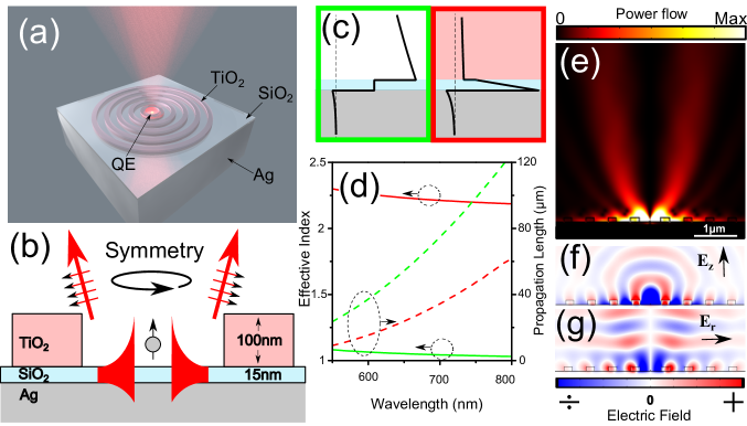
The general operation of our device is conceptually illustrated in figure 1(a,b). A QE, centered in the bullseye antenna in close proximity to the silver film, spontaneously decays by excitation of surface plasmon polaritons (SPP) propagating along the dielectric-metal interface. The SPP subsequently scatter directionally on the periodically spaced TiO2 ridges, resulting in highly directional emission.
The emission of a QE or electric dipole, situated in close proximity to a silver film, has been thoroughly studied22 and analytically described 23, 24. It is thus well known that dipole emission is accelerated when the dipole is oriented normal to the metal plane, as emission is efficiently coupled into SPP. On the other hand, when the dipole is oriented along the plane, emission is suppressed, as the dipole induces a mirrored anti-phase charge distribution in the silver film (see Support Information (SI)). In the present study we thus neglect the weak in-plane dipole emission, and model QE emission solely in terms of the dominating vertical dipole (figure 1b). Placing the dipole along the symmetry z-axis, our system reduces to a cylindrical symmetric system, for which we assume a constant azimuthal phase, as no particular phase preference can be expected. In other words, the emission field is assumed to be unchanged upon rotation about the z-axis. Clearly, in this case the radial electric field component is singular on the symmetry axis, and must therefore be zero (figure 1g). The condition prohibits emission along the symmetry axis, as the transverse field of a plane wave, propagating along the symmetry axis, must be zero. The rotational symmetry of dipole source and antenna is thus expected to result in a radially polarized emission field, for which emission normal to the silver film is prohibited, regardless of emission wavelength.
With the symmetry constraints in place, we now seek to maximize dipole emission into the 0.9 NA objective, at the target wavelength of 670 nm, by introducing a dielectric grating for scattering of SPP coupled emission. In order to maximize antenna efficiency, we seek to minimize SPP propagation loss by employing a high-index TiO2 grating (n=2.2 index, measured with ellipsometry see SI), separated from the silver film by a thin low-index SiO2 spacer layer (n=1.45 index). The SPP mode of the high index-low index spacer - on conductor configuration25 is recieving increasing interest as a possible approach for low-loss plasmonics26, 27. Analytical solutions for the SPP mode supported by the 3-layer structure (figure 1 c,d) reveal large modulation of the effective index from 1.05 (Air-SiO2-Ag) to 2.25 (TiO2-SiO2-Ag), with propagation lengths of respectively L=63 and L=28 far exceeding lateral antenna dimensions. SPP coupled emission is thus prone to either scatter on the TiO2 grating or reflect back to the emitter, while propagation losses are minimal. For fabrication purposes, we set titania and silica film thicknesses to 100 nm and 15 nm respectively, and numerically optimize in-plane grating parameters for collecting the maximal amount of dipole power with a 0.9 NA objective (see SI for optimization procedure). The inner TiO2 ridge (inner radius 250 nm, TiO2 width 212 nm) in this case forms a standing wave cavity (figure 1f), accelerating dipole emission by a decay rate enhancement of 18 (relative to vacuum). Simultaneously, the periodic TiO2 grating (period 520 nm, duty cycle 0.36), directionally scatters SPP coupled emission, such that 85 of the power emitted by the dipole is collected by the objective. While on-resonance SPP emission is scattered at an angle near normal to silver plane (figure 1 e,g), the scattering angle generally seems to follow the grating equation (see SI for comparison). The geometrical optimization of TiO2 height is a trade-off between decay rate enhancement and collection efficiency. Collection efficiency defined as the fraction of the total dipole power, collected by the objective, while decay rate enhancement is the factor by which the total dipole emission power increases in the bullseye environment, relative to vaccum.
Indeed, a significant increase in decay rate enhancement is possible by increasing the TiO2 thickness (see SI for modelling) at the cost of collection efficiency, as the SPP perform an increasing number of lossy round trips in the cavity before scattering to free space. For practical fabrication purposes, the low aspect ratio design of 100 nm TiO2 was preferred, while the 15 nm SiO2 film thickness was set to ensure a homogenous coverage of the silver film, for environmental protection of the silver.
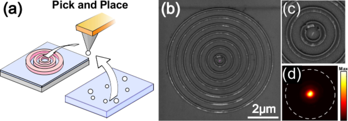
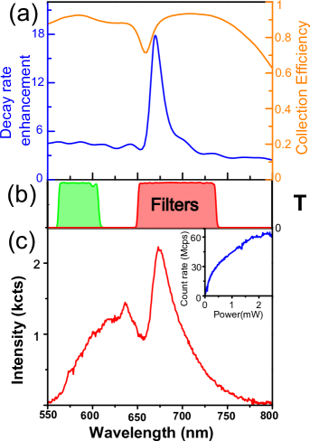
The bullseye antenna sample was fabricated on a Si substrate by e-beam evaporation of 10 nm Ti, 3 nm Ge followed by a 200 nm Ag film and topped by a 15 nm SiO2 layer, without breaking the vacuum. The 100 nm TiO2 bullseye grating was subsequently formed by standard electron beam lithography and e-beam evaporation (figure 2b). Importantly, device performance was not degraded by the use of any lossy adhesion layers at the Ag-SiO2-TiO2 interfaces, while remaining mechanically robust to sonication, applied during lift-off. A ND (length 140 nm , height 35 nm) containing a large number of NV-centers was subsequently picked up from a coverslip and placed in the center of the bullseye antenna, using an atomic force microscope (AFM) (figure 2a). The AFM "pick and place" technique28 allows for precise centering of the ND, as confirmed by electron microscopy (figure 2d). Pumping the ND with a 532 nm continuous-wave laser, we image the NV-center fluorescence onto a CCD camera, using a 0.9 NA x100 objective and fluorescence filtering from a dichroic mirror (cut-off 550 nm) and long pass filter (cut-off 550 nm) (see SI for schematic of setup). The NV-center emission is observed as a spot, tightly confined to the center of bullseye antenna, indicating efficient scattering of SPP-coupled emission on the TiO2 ridges (figure 2c). Correspondingly, antennas without a ND appear dark, when mapping fluorescence by laser-scanning confocal microscopy (see SI for comparison). In order to observe the wavelength dependent decay rate enhancement, expected from numerical modelling (figure 3a), the NV-center emission was spectrally resolved on a grating spectrometer (Figure 3c). The zero phonon lines (ZPL) for the neutral- (575 nm) and negative (637 nm) charge states confirm the NV-center as the origin of fluorescence, while the overall spectrum is dominated by a resonant enhancement peak at 675 nm, in reasonable agreement with the modelled decay rate enhancement. The experimental quality factor of 18 (estimated from spectrum) is broader than the modelled resonance 41 (estimated from decay rate enhancement curve), presumably due to fabrication imperfections. Collection efficiency is not expected to significantly affect the spectrum, as modelling finds overall high broadband collections efficiency (figure 3a), stemming from emission into SPP and grating scattering of SPP into objective both being broadband effects.
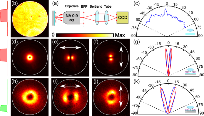
For efficient photon generation, it is typically desired to maximize photon rate from the QE, by pumping the QE to saturation. We confirmed that our device is stable under such conditions by increasing laser power to the 2.5 mW limit of our equipment. Simultaneously monitoring the photon rate detected by a avalanche photo diode, we smoothly transition to stable operation at saturation (figure 3c inset). Subsequently reducing laser power, we retrace the saturation curve, thereby confirming no antenna alterations. The planar film bullseye antenna is generally expected to exhibit a higher laser damage threshold, than structured film configurations, as nanostructuring of metals suffer from melting point depression29. Having confirmed stable operation at saturation laser power and the presence of resonantly enhanced emission, we proceed by examining the off- and on-resonance emission pattern, selected with bandpass filter in the wavelength range 560-610 nm and 650-740 nm (figure 3b). Introducing a bertrand lens in infinity space, we resolve the emission pattern by imaging the back-focal plane(BFP) of the objective onto the CCD camera (figure 4a). This lens configuration is particularly well suited for fourier microscopy30. Filtering for resonant emission reveals a highly directional radiation pattern in the characteristic donut-shaped pattern, imposed by the antenna symmetry (figure 4d). Introducing an analyzer in the optical path, the radiation is confirmed to be radially polarized (figure 4 e,f). This is apparent as emission is spatially extinquished along the axis normal to the analyzer axis for a random analyzer orientation. For a comparison with the numerical design, we extracted the angular radiation pattern from a single pixel slice of the BFP-image, finding the experiment generally replicates numerical expectations. On resonance, the peak emission is detected at an angle of 5 FWHM wrt. the plane normal, in good agreement with the designed emission angle of 6 FWHM, modelled for the resonance wavelength of 670 nm (figure 4g). Probing off-resonant emission, we find the peak emission increasing to an angle of 14 FWHM (figure 4k), while the symmetry conditioned, radially polarized donut shaped beam pattern is conserved (figure 4h-j). Off-resonance emission is in line with the modelled emission for a wavelength of 610 nm having peak emission at an angle of 16. Off-resonance emission is modelled at the wavelength of 610 nm, as experimentally, the maximum spectral power transmitted by the band-pass filter is found at this wavelength (figure 3c).
The directional emission is in stark contrast to the omni-directional emission of the same type of ND, when situated on a coverslip (figure 4b,c).
The relatively narrowband decay rate enhancement and directive emission, demonstrated for this design, may be of interest for indistinguisable photon experiments, as the selective enhancement and efficient collection of ZPL photons from solid state emitters is desirable. The simple fabrication allows for easy tuning of the antenna resonance to the ZPL of new promising QEs such as the silicon- or germanium vacancy centers 31, 32. However, for scalable single photon source fabrication, large-scale QE positioning techniques need to be explored. Potential approaches may be lithographic patterning33 or electro-static pad positioning34. Further, the highly directional emission pattern should lend itself to optical fiber coupling. Theoretically, 23 and 74 of dipole emission (wavelength 670 nm) fall within the numerical aperture of respectively a single- (NA 0.12) or multi-mode fiber (NA 0.4). It is in this context worth noting that the radially polarized emission pattern, inherent to the bullseye antenna, may be converted to the fundamental mode of an optical fiber with high fidelity35. Directive emission is further advantageous for NV ensemble-based sensing applications, relying on optical read-out of the NV-center spin state, where strong decay rate enhancement should be avoided.3 The design may potentially be optimized for operation in an oil index matching environment, to limit reflection losses at the fiber or objective input.
3 Conclusion
In summary, we have proposed a high-efficiency hybrid plasmonic bullseye antenna design, consisting of a high-index titania grating, separated from a planar silver film by a thin low-index silica spacer layer. The architecture is motivated by previous issues with background emission resulting from nanostructuring of silver films. Our design combines low antenna loss, directional emission and moderate decay rate enhancement, leading to a theoretical collection efficiency of 85% for a 0.9 NA objective and acceleration of the emission rate by a decay rate enhancement of 18, at the design wavelength of 670 nm. The design is experimentally realized by standard electron beam lithography, followed by deterministic placement of a fluorescent ND in the bullseye, using the AFM "pick and place" technique. The particular material design allows for fabrication without lossy adhesion layers compromising device performance, and stable operation of the antenna at laser powers large enough for saturated pumping of the NV-centers contained in the ND. Decay rate enhancement is experimentally observed as a resonant peak in the NV-center emission spectrum at 675 nm (quality factor 18). The resonantly filtered fluorescence is demonstrated to be highly directional by back-focal plane imaging, with peak emission at an angle of 5∘ with respect to plane normal. Specifically, the emission pattern takes the form of a donut-shaped, radially polarized beam as imposed by the antenna symmetry, regardless of emission wavelength. Experimental observations closely mimic the numerical design, thereby validating the proposed design. The demonstrated design is significant for quantum technological development, as light-matter interfaces ensuring efficient photon collection from single QEs are highly desirable for quantum optical applications.
Methods
Sample Preparation
The bullseye antenna was fabricated by successive electron-beam evaporation of 10 nm Ti, 3 nm Ge, 200 nm Ag topped by 15 nm SiO2 on a Si wafer, at a deposition rate of 1 Å/s and mbar chamber pressure, without breaking the vacuum. PMMA 4A was spincoated at 4000 rpm on the sample, and prebaked at 180 Co for 3 min before patterning by a 100kV electron beam lithography system (Leica VB6). After development (1:3 MIBK-to-IPA for 1 min followed by 1 min rinse in IPA), a 100 nm TiO2 layer was deposited by electron-beam evaporation at 1 Å/s and mbar pressure. Lift-off in acetone at 60 for 5 h was partially successful, as subsequently 5 min of sonication in acetone was required to remove PMMA between the TiO2 ridges to reveal the bullseye. In preparation of ND placement, 100 nm ND’s containing 400 NV-centers (Adamas technology) was spincoated on a coverslip, previously cleaned in piraniha etch (Nanostrip x2 - KMG electronic chemicals). To ease the transfer, the bullseye sample was coated with a 2 nm thick layer of positively charged poly-allylamine hydrochloride (PAH) layer. ND pick-up was performed by a force curve sequence, with the AFM cantilever situated above the ND. Successful pick-up was confirmed by a subsequent non-contact scan. Exchanging samples, a force curve was performed in the center of the bullseye, followed by an AFM scan to confirm the placement of the ND.
Numerical Modelling
Numerical modelling was performed in the commercially available Comsol Multiphysics 5.1. The full 3-D field of the axial symmetric system is numerically modelled by solving a 2-D slice, on the assumption of a constant azimuthal phase. The limited computational requirements of 2-D modelling, allowed us to model the full bullseye antenna, in a domain of radius 22, bounded from the top by a perfectly matched layer and below by the silver film. Material parameters for silver were obtained for tabulated data 36, while TiO2 data was measured by ellipsometry (see SI) and a refractive index of 1.45 was set for SiO2. The emission field was generated by an electric dipole source positioned on the symmetry axis, 15 nm above the SiO2 film. The decay rate enhancement was obtained as the total power dissipated by the dipole in the bullseye environment, relative to that of free space. Collection efficiency was obtained as the power integrated over a 0.9 NA collection surface, relative to the total power dissipated by the dipole. The radiation pattern was obtained by plotting the Poynting vector over a spherical arc in the 2-D plane.
Experiment
The ND was excited with a 532 nm continous wave laser, focused onto the sample by a 0.9 NA x100 objective which was mounted on a piezo-stage for fine positioning of laserspot. Fluorescence collected by the same objective was filtered by a 550 nm dichroic mirror (DMLP550L-Thorlabs) and 550 nm long pass filter (FEL0550- Thorlabs), before being directed to a spectrometer (QE65000 - Ocean Optics) or avalance photodiode (SPCM-AQRH - Excelitas) in a confocal detection configuration using a 50 pinhole. Alternatively fluorescence was detected by a charge coupled camera (414Ex - Atik Cameras) imaging sample plane (using a 20 mm tube lens) or back-focal plane (600 mm bertrand- and 75 mm tube lens) onto the camera. off- or on-resonance emission was selected by filters of respectively 560-610 nm and 650-740 nm transmission bands, while an analyzer (LPVISC050-MP2 - Thorlabs) was introduced to probe polarization. Back-focal plane images from bullseye antenna, was background corrected for a corresponding image from an empty antenna. Saturation curve measurement was performed with a ND2 filter positioned infront of the avalance photodiode, the presented count rate was corrected for transmission of ND2 filter and the pinhole. See SI for a schematic of experimental setup. {acknowledgement} The authours gratefully acknowledge the finanical support of the European Research Council (Grant 341054 (PLAQNAP)), Georgia St. (Grant 106806), MRSEC (Grant 105675), ONR-DURIP (Grant No. N00014-16-1-2767), AFOSR-MURI (Grant No. FA9550-14-10389) and DOE (Grant DE-SC0017717).
The following files are available free of charge. S1: Analytical model of electric dipole above silver film. S2: Ellipsometry measurement of TiO2 refractive index. S3: Numerical optimization procedure of bullseye antenna. S4: Comparision of bullseye emission angle with grating equation. S5: Optimized antenna design for different TiO2 heights. S6: Schematic of experimental setup. S7: Confocal scan of bullseye antenna with- and without ND.
References
- O’Brien et al. 2009 O’Brien, J. L.; Furusawa, A.; Vuckovic, J. Photonic quantum technologies. Nat Photon 2009, 3, 687–695
- Steiner et al. 2010 Steiner, M.; Neumann, P.; Beck, J.; Jelezko, F.; Wrachtrup, J. Universal enhancement of the optical readout fidelity of single electron spins at nitrogen-vacancy centers in diamond. Phys. Rev. B 2010, 81, 035205
- Bogdanov et al. 2017 Bogdanov, S.; Shalaginov, M. Y.; Akimov, A.; Lagutchev, A. S.; Kapitanova, P.; Liu, J.; Woods, D.; Ferrera, M.; Belov, P.; Irudayaraj, J.; Boltasseva, A.; Shalaev, V. M. Electron spin contrast of Purcell-enhanced nitrogen-vacancy ensembles in nanodiamonds. Phys. Rev. B 2017, 96, 035146
- Bernien et al. 2012 Bernien, H.; Childress, L.; Robledo, L.; Markham, M.; Twitchen, D.; Hanson, R. Two-Photon Quantum Interference from Separate Nitrogen Vacancy Centers in Diamond. Phys. Rev. Lett. 2012, 108, 043604
- Sipahigil et al. 2014 Sipahigil, A.; Jahnke, K. D.; Rogers, L. J.; Teraji, T.; Isoya, J.; Zibrov, A. S.; Jelezko, F.; Lukin, M. D. Indistinguishable Photons from Separated Silicon-Vacancy Centers in Diamond. Phys. Rev. Lett. 2014, 113, 113602
- Aharonovich et al. 2016 Aharonovich, I.; Englund, D.; Toth, M. Solid-state single-photon emitters. Nat Photon 2016, 10, 631–641
- Kinkhabwala et al. 2009 Kinkhabwala, A.; Yu, Z.; Fan, S.; Avlasevich, Y.; Mullen, K.; E., M. Large single-molecule fluorescence enhancements produced by a bowtie nanoantenna. Nat Photon 2009, 3, 654–657
- Barnes et al. 2002 Barnes, W.; Björk, G.; Gérard, J.; Jonsson, P.; Wasey, J.; Worthing, P.; Zwiller, V. Solid-state single photon sources: light collection strategies. The European Physical Journal D - Atomic, Molecular, Optical and Plasma Physics 2002, 18, 197–210
- Schell et al. 2014 Schell, A. W.; Neumer, T.; Shi, Q.; Kaschke, J.; Fischer, J.; Wegener, M.; Benson, O. Laser-written parabolic micro-antennas for efficient photon collection. Applied Physics Letters 2014, 105, 231117
- Jamali et al. 2014 Jamali, M.; Gerhardt, I.; Rezai, M.; Frenner, K.; Fedder, H.; Wrachtrup, J. Microscopic diamond solid-immersion-lenses fabricated around single defect centers by focused ion beam milling. Review of Scientific Instruments 2014, 85, 123703
- Curto et al. 2010 Curto, A. G.; Volpe, G.; Taminiau, T. H.; Kreuzer, M. P.; Quidant, R.; van Hulst, N. F. Unidirectional Emission of a Quantum Dot Coupled to a Nanoantenna. Science 2010, 329, 930–933
- Lee et al. 2011 Lee, K. G.; Chen, X. W.; Eghlidi, H.; Kukura, P.; Lettow, R.; Renn, A.; Sandoghdar, V.; Gotzinger, S. A planar dielectric antenna for directional single-photon emission and near-unity collection efficiency. Nat Photon 2011, 5, 166–169
- Li et al. 2015 Li, L.; Chen, E. H.; Zheng, J.; Mouradian, S. L.; Dolde, F.; Schröder, T.; Karaveli, S.; Markham, M. L.; Twitchen, D. J.; Englund, D. Efficient Photon Collection from a Nitrogen Vacancy Center in a Circular Bullseye Grating. Nano Letters 2015, 15, 1493–1497
- Davanço et al. 2011 Davanço, M.; Rakher, M. T.; Schuh, D.; Badolato, A.; Srinivasan, K. A circular dielectric grating for vertical extraction of single quantum dot emission. Applied Physics Letters 2011, 99, 041102
- Aouani et al. 2011 Aouani, H.; Mahboub, O.; Bonod, N.; Devaux, E.; Popov, E.; Rigneault, H.; Ebbesen, T. W.; Wenger, J. Bright Unidirectional Fluorescence Emission of Molecules in a Nanoaperture with Plasmonic Corrugations. Nano Letters 2011, 11, 637–644
- Jun et al. 2011 Jun, Y. C.; Huang, K. C.; Brongersma, M. L. Plasmonic beaming and active control over fluorescent emission. ncomms 2011, 2, 1–6
- Choy et al. 2013 Choy, J. T.; Bulu, I.; Hausmann, B. J. M.; Janitz, E.; Huang, I.-C.; Loncar, M. Spontaneous emission and collection efficiency enhancement of single emitters in diamond via plasmonic cavities and gratings. Applied Physics Letters 2013, 103, 161101
- Livneh et al. 2016 Livneh, N.; Harats, M. G.; Istrati, D.; Eisenberg, H. S.; Rapaport, R. Highly Directional Room-Temperature Single Photon Device. Nano Letters 2016, 16, 2527–2532
- Livneh et al. 2015 Livneh, N.; Harats, M. G.; Yochelis, S.; Paltiel, Y.; Rapaport, R. Efficient Collection of Light from Colloidal Quantum Dots with a Hybrid Metal Dielectric Nanoantenna. ACS Photonics 2015, 2, 1669–1674
- Kumar et al. 2012 Kumar, S.; Lu, Y.-W.; Huck, A.; Andersen, U. L. Propagation of plasmons in designed single crystalline silver nanostructures. Opt. Express 2012, 20, 24614–24622
- Park et al. 2012 Park, J. H.; Ambwani, P.; Manno, M.; Lindquist, N. C.; Nagpal, P.; Oh, S.-H.; Leighton, C.; Norris, D. J. Single-Crystalline Silver Films for Plasmonics. Advanced Materials 2012, 24, 3988–3992
- Drexhage 1970 Drexhage, K. Influence of a dielectric interface on fluorescence decay time. Journal of Luminescence 1970, 1, 693 – 701
- Ford and Weber 1984 Ford, G.; Weber, W. Electromagnetic interactions of molecules with metal surfaces. Physics Reports 1984, 113, 195 – 287
- Chance et al. 1978 Chance, R. R.; Proc, A.; Silbey, R. Molecular fluorescence and energy transfer near interfaces. Adv. Chem. Phys 1978, 37, 1 – 34
- Avrutsky et al. 2010 Avrutsky, I.; Soref, R.; Buchwald, W. Sub-wavelength plasmonic modes in a conductor-gap-dielectric system with a nanoscale gap. Opt. Express 2010, 18, 348–363
- Cui et al. 2015 Cui, S.; Zhang, X.; Liu, T.-l.; Lee, J.; Bracher, D.; Ohno, K.; Awschalom, D.; Hu, E. L. Hybrid Plasmonic Photonic Crystal Cavity for Enhancing Emission from near-Surface Nitrogen Vacancy Centers in Diamond. ACS Photonics 2015, 2, 465–469
- Yang et al. 2017 Yang, Y.; Miller, O. D.; Christensen, T.; Joannopoulos, J. D.; Soljačić, M. Low-Loss Plasmonic Dielectric Nanoresonators. Nano Letters 2017, 17, 3238–3245
- Schell et al. 2011 Schell, A. W.; Kewes, G.; Schröder, T.; Wolters, J.; Aichele, T.; Benson, O. A scanning probe-based pick-and-place procedure for assembly of integrated quantum optical hybrid devices. Review of Scientific Instruments 2011, 82, 073709
- Jiang et al. 2003 Jiang, Q.; Zhang, S.; Zhao, M. Size-dependent melting point of noble metals. Materials Chemistry and Physics 2003, 82, 225 – 227
- Kurvits et al. 2015 Kurvits, J. A.; Jiang, M.; Zia, R. Comparative analysis of imaging configurations and objectives for Fourier microscopy. J. Opt. Soc. Am. A 2015, 32, 2082–2092
- Neu et al. 2011 Neu, E.; Steinmetz, D.; Riedrich-Möller, J.; Gsell, S.; Fischer, M.; Schreck, M.; Becher, C. Single photon emission from silicon-vacancy colour centres in chemical vapour deposition nano-diamonds on iridium. New Journal of Physics 2011, 13, 025012
- Iwasaki et al. 2015 Iwasaki, T. et al. Germanium-Vacancy Single Color Centers in Diamond. Sc. Rep 2015, 5, 12882
- Manfrinato et al. 2013 Manfrinato, V. R.; Wanger, D. D.; Strasfeld, D. B.; Han, H.-S.; Marsili, F.; Arrieta, J. P.; Mentzel, T. S.; Bawendi, M. G.; Berggren, K. K. Controlled placement of colloidal quantum dots in sub-15 nm clusters. Nanotechnology 2013, 24, 125302
- Jiang et al. 2015 Jiang, M.; Kurvits, J. A.; Lu, Y.; Nurmikko, A. V.; Zia, R. Reusable Inorganic Templates for Electrostatic Self-Assembly of Individual Quantum Dots, Nanodiamonds, and Lanthanide-Doped Nanoparticles. Nano Letters 2015, 15, 5010–5016
- Ramachandran et al. 2009 Ramachandran, S.; Kristensen, P.; Yan, M. F. Generation and propagation of radially polarized beams in optical fibers. Opt. Lett. 2009, 34, 2525–2527
- Johnson and Christy 1972 Johnson, P. B.; Christy, R. W. Optical Constants of the Noble Metals. Phys. Rev. B 1972, 6, 4370–4379