An electron acceptor molecule in a nanomesh: F4TCNQ on -BN/Rh(111)
Abstract
The adsorption of molecules on surfaces affects the surface dipole and thus changes in the work function may be expected. The effect in change of work function is particularly strong if charge between substrate and adsorbate is involved. Here we report the deposition of a strong electron acceptor molecule, tetrafluorotetracyanoquinodimethane C12F4N4 (F4TCNQ) on a monolayer of hexagonal boron nitride nanomesh (-BN on Rh(111)). The work function of the F4TCNQ/-BN/Rh system increases upon increasing molecular coverage. The magnitude of the effect indicates electron transfer from the substrate to the F4TCNQ molecules. Density functional theory calculations confirm the work function shift and predict doubly charged F4TCNQ2- in the nanomesh pores, where the -BN is closest to the Rh substrate, and to have the largest binding energy there. The preferred adsorption in the pores is conjectured from a series of ultraviolet photoelectron spectroscopy data, where the bands in the pores are first attenuated. Scanning tunneling microscopy measurements indicate that F4TCNQ molecules on the nanomesh are mobile at room temperature, as ”hopping” between neighboring pores is observed.
keywords:
electron acceptor , charge transfer , work function , -BN , STMIntroduction
Electron transfer is an essential process that governs many elementary processes in physics and chemistry. For atomic or molecular adsorbates on metallic surfaces simple arguments predict on whether charge is transferred from the surface to the molecule or vice versa. The relevant quantities are the work function of the surface and on the other hand the ionisation potential or electron affinity of the atom or molecule: If the work function is larger than the ionisation potential, an electron is transferred to the metal substrate and the adsorbate charges positively. This effect is well known and e.g. used for surface ionisation of alkali metal atoms [1]. If the electron affinity is larger than the work function, an electron is transferred to the adsorbate from metal substrate [2]. In the case of surface ionisation it was pointed out by Gurney [3] that the quantum mechanical broadening of the adsorbate orbitals lead to the situation where the charge transfer is not complete and thus the electron tunnels back and forth between adsorbate and substrate. Also, the distance dependent interaction between substrate and adsorbate leads to a variation of the ionisation potential and the electron affinity, and the charge transfer itself changes the work function of the surface locally.
The charge transfer due to polarisation may be inferred from the induced change in the surface dipole. If the adsorbate density is known, the induced dipole may be determined from the Helmholtz equation that relates a change of the work function with the areal density or coverage of the dipoles induced by the adsorbed species:
| (1) |
where is the elementary charge, the induced dipole parallel to the surface normal, and the vacuum permittivity. From Eq. 1 we see that the work function decreases if charge is transferred to the surface and oppositely increases if charge is transferred to the molecule.
If the metal surface is covered with a single layer graphite (graphene, ) [4, 5] or hexagonal boron nitride (-BN) [6], the reactivity of the system changes. In particular, the charge transfer time across the layer increases, and non-adiabatic effects may be observed [7].
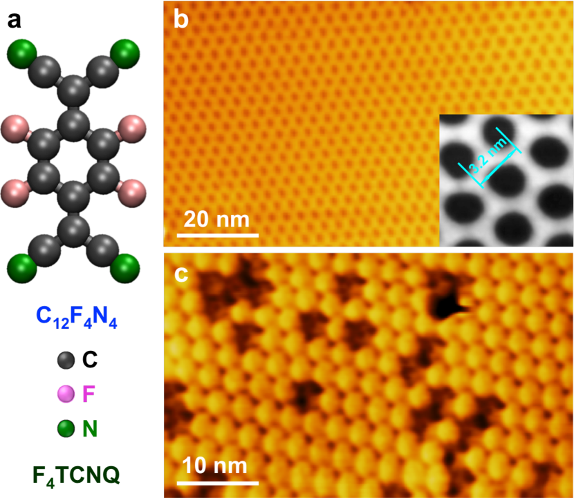
The high electron affinity of the tetrafluorotetracyanoquinodimethane C12F4N4 (F4TCNQ; see the chemical structure in Figure 1a) has made it to be a frequently employed electron acceptor molecule, with which anion formation on surfaces may be studied. Previously, Barja et al. reported self assembly of TCNQ (C12H4N4) and F4TCNQ (C12F4N4) on the graphene/iridium system [8]. At low temperatures different adsorption geometries and electronic properties, depending on where the molecules were located in the /Ir(111) unit cell [9].
The electron affinity of F4TCNQ is 5.2 eV [10] and exceeds the work function of the -BN/Rh(111) nanomesh [11] by 1.05 eV. Therefore we expect a complete electron transfer onto the molecule, and the formation of an open shell electronic system. This would open perspectives for spintronics as it was put forward for the TCNQ//Ru(0001) where long range magnetic order was found [12].
Here we report on F4TCNQ on the -BN nanomesh on Rh(111). We have investigated the system with photoemission spectroscopy and scanning tunnelling microscopy (STM) on the same preparations. Density functional theory (DFT) calculations complement the picture and come up with an unexpected prediction of structures with high adsorption energy and transfer of more than one electron onto the molecule.
The substrate in this study is the -BN nanomesh on Rh(111) [13]. It features a corrugated single layer of boron nitride [14], where 1313 BN units form a coincidence lattice on 1212 Rh units with the nearest neighbour distances (Figure 1b). The 1212 unit cell is constituted by 2 nm pores, where the nitrogen atoms are close to on-top Rh configuration, and where nitrogen lone pair bonding occurs [15]. These pores are separated by ”wire” regions where the interaction of the -BN with the substrate is weak. This pore-wire structure imposes strong lateral electrical fields (dipole rings) that are due to variations of the local electrostatic potential and that lead to to the self assembly of molecules in the pores [11]. The electrostatic landscape is such that negative charge is attracted to the pores, and accordingly we expect F4TCNQ to first occupy the pores.
Results and Discussion
Figure 1b displays STM images of the pristine -BN nanomesh on Rh(111) substrate with a superstructure lattice constant of 3.2 nm (shown in the inset of Figure 1b). In Figure 1c an STM image of the -BN/Rh(111) nanomesh after a small dose of F4TCNQ with less than 1 molecule per nanomesh unit cell is shown, which corresponds to the data point marked with green square in Figure 2a. ”Bright” protrusions and ”dark” depressions are imaged with the periodicity of the nanomesh. This imaging condition is obtained on a regular base after scanning the surface for some time at room temperature. The picture resembles the STM image of F4TCNQ on /Ir(111), where the protrusions have been assigned to the molecules [8]. The ratio between dark and bright pores and comparison to the coverage as determined via the X-ray photoemission spectroscopy (XPS) and the work function shift of 80 meV that were measured on the same sample rather favors a picture where the dark pores correspond to pores that are occupied with a molecule.
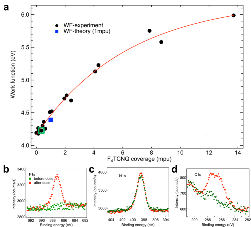
Figure 2 shows the work function of the F4TCNQ/-BN/Rh(111) system as obtained from the width of He I excited normal emission ultraviolet photoemission spectra (UPS) as a function of molecular coverage . The coverage, given in units of molecules per nanomesh unit cell (mpu), has been determined from Mg K excited XPS intensity ratios between the F 1s, the N 1s and the C 1s peaks and the corresponding atomic photoemission cross sections, as shown at a coverage of 7.8 mpu in Figure 2b-2d. Accordingly we find a coverage of one F4TCNQ mpu at an atomic F:N ratio of 4:173. Furthermore we note that the splitting in the C 1s emission indicates the existence of chemically different carbon species in the molecule.
As expected for an electron transfer to the molecules the work function increases with coverage. Fitting the data in Figure 2a to the function we obtain the red line in Figure 2a and parameters eV, eV, and 6.4 mpu. From this we see that at coverages below 2 mpu the work function increases linearly. The work function shift is much more pronounced than in the F4TCNQ//SiC system where Chen et al. found an increase of 0.7 eV [16]. Given the fact that the work function of /SiC is similar to that of -BN/Rh(111) this is an indication that the binding of F4TCNQ is different to -BN on a metal from on a semiconductor. For 1 mpu we obtain a work function shift of 0.3 eV at room temperature, and in cooling the sample to 185 K the work function further increases by 50 meV. The temperature dependent work function shift may be due to a higher occupancy in the pores. These values can be compared to the result from the DFT calculations, where we obtain a value of 0.19 eV as indicated with the blue square in Figure 2a. We consider this a very good agreement with experimental confirmation that at low coverage F4TCNQ- anions are formed on the -BN nanomesh.
Figure 3 shows normal emission He I UPS excited valence band photoemission data of F4TCNQ on -BN/Rh(111) as a function of the coverage . In Figure 3a a series of UPS spectra at different F4TCNQ coverages from 0 to 4.3 mpu are shown. The spectrum at =0 mpu is recorded after annealing the clean nanomesh. Afterwards F4TCNQ has been evaporated successively and measured with XPS and UPS after each evaporation. The spectra are dominated by the well-known valence band pattern of -BN/Rh(111) with the Rh 4d valence band peak at 0.88 eV binding energy, and the split -BN -band [14]: that accounts for the electronic structure in the nanomesh wires and for that in the nanomesh pores [17].
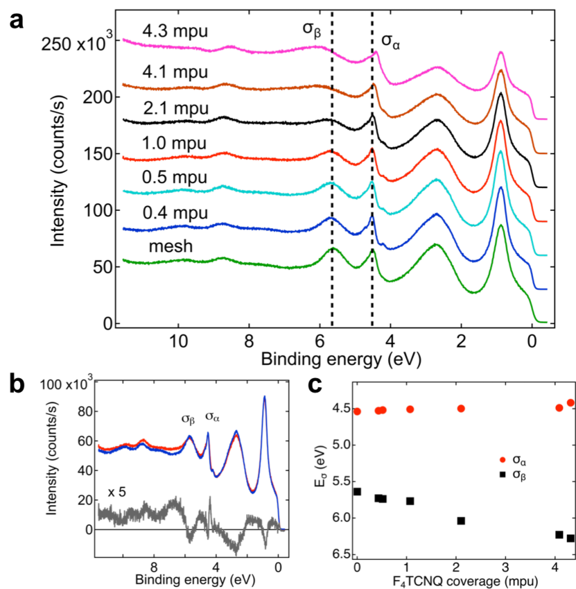
Like it was first shown for naphthalocyanine on -BN nanomesh [14] and later for Xe on -BN nanomesh [11], adsorbates attenuate the photoemission signals from the substrate, and since the signal from the pore, is attenuated before the signal from the wires , a higher adsorption energy in the pores was concluded for naphthalocyanine and for 12 Xe atoms in the pores. Here we observed the same trend: With increasing molecular coverage the intensity decreases before it does the same in the the intensity. In Figure 3b the spectra of 0.4 mpu and 1.0 mpu are compared, and the difference between the two (1.0 mpu - 0.4 mpu) is displayed after scaling by a factor of 5. The above-said is confirmed, in particular the attenuation effect is also seen for the Rh substrate peaks.
The assignment of molecular orbitals is not possible at these low coverages, photon energy and emission angle. We observe, however, a shift in binding energy for the boron nitride related bands. The sharpest feature in the difference curve lies at the steep onset of the band at 4.39 eV binding energy and it is accompanied by a sharp negative peak at 4.53 eV. This indicates a band shift to lower binding energy with increasing coverage and is remarkable since the majority of the molecules must occupy the pores, as implied by the attenuation of the intensity. The spectral weight near the broader peak appears to shift towards higher binding energies with increasing coverage. This may be related to the decrease intensity and the increase of F4TCNQ derived molecular orbitals at around 7 eV binding energy. In Figure 3c the binding energy positions of the band and the local maximum near the band are shown as a function of the F4TCNQ coverage. For flat -BN the sigma bands are known to align with the vacuum level and to lead to the ”physisorption model” [6], where on the Rh(111) substrate the band has the same offset of about 9 eV from the vacuum level like on Ni, Pd and Pt. Therefore it is expected that with increasing work function the energy rises. The fact that the rise of 14 meV per mpu does not correspond to the 300 meV per mpu indicates again that the vast majority of the F4TCNQ molecules are not adsorbed on the wires. The shift in band of -161 meV per mpu may not be explained with the -BN ”physisorption model” of Nagashima et al. [6]. It rather indicates that the F4TCNQ- molecules influence the boron and the nitrogen atoms in the pore, and the above-mentioned photoemission intensity redistribution between and F4TCNQ molecular orbitals that may impose as well an apparent shift.
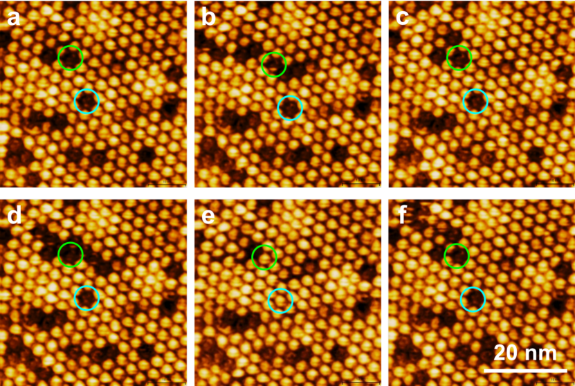
Figure 4 shows STM images of a sample at low coverage measured with variable temperature (VT-)STM system. As mentioned above, low coverage of F4TCNQ/-BN/Rh(111) displays ”bright” and ”dark” features on the -BN surface at room temperature, which are confirmed by two different instruments, i.e., electron spectroscopy for chemical analysis (ESCA) Park Scientific (Figure 1c) and VT-STM (Figure 4). Figures 4a-4f illustrate a sequence of continuous scanning of the same area with same scanning conditions, where the time intervals between the images is 125 s. The green and blue circles in each image indicate the same positions individually in order to guide the eyes. The 6 images evidently demonstrate F4TCNQ ”hopping” on the -BN surface at room temperature. For instance, the ”dark” depressions marked with green and blue circles in Figure 4d appear to be ”bright” protrusions in the Figure 4e, while the same positions show the ”dark” features again in the subsequent Figure 4f. In order to demonstrate more ”hopping” events and in a longer time interval, we made a movie with 40 continuous STM images scanning with same condition on the same area in the Supporting Information. This ”hopping” indicates high mobility of F4TCNQ molecules on -BN surface, which is similar to the case of F4TCNQ on /Ir, where the F4TCNQ molecules were reported to ”rotate” even at 77 K [8].
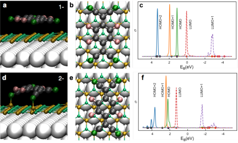
To better understand the experimental results, we carried out DFT calculations. Because the molecular orbitals (for example the highest occupied molecular orbital, HOMO) preserve their character in the free molecule to a large extent, in the following we refer to those orbitals as in the neutral gas-phase molecule, even whn the initial lowest unoccupied molecular orbital (LUMO) gains electrons, to simplify the discussion. The DFT results confirm that the F4TCNQ molecules like to occupy the pore of the -BN nanomesh. The theory predicts the work function change and the charge transfer upon adsorption of one mpu. In Figure 5 the two lowest energy structures in the nanomesh pores are depicted. They are significantly distinct to each other, in binding energy, charge transfer, work function change and coordination to the beneath -BN. In reference to the charge transfer the two structures are labeled as ”” and ””. Intriguingly, the work function change of ”” is smaller than that of the ”” structure, which must be related to the onset of covalent chemisorptive bonds and gain of exchange energy in the LUMO in ””, which apparently superseeds the Coulomb repulsion in the LUMO. On the other hand ”” is more physisorptive with ionic and van der Waals bond character and an open LUMO shell. The work function change of 0.19 eV per mpu of the lowest energy ”” structure fits well to the experimental result of 0.3 eV. Though, from the experiment we find no direct arguments on the charge state of F4TCNQ on -BN nanomesh. Rather, the high DFT binding energy difference between molecules in the pore and on the wire (see Table 1), would not suggest much diffusion as we observe it at room temperature. We have to speculate on how the detailed hopping mechanism as we observe it (see Figure 4) operates: Possibly the STM imaging process triggers hopping events. In Figure 5c and 5f the orbital overlap , or the projection of the Kohn-Sham electronic states of the adsorption system on the molecular orbitals of a single molecule (but in the geometry as adsorbed) is shown for ”” and ””. The orbital overlap indicates at which energies the molecular orbitals reside when adsorbed, and if there are large changes, for example due to hybridisation. There are clearly defined states, in particular the HOMO1, HOMO and LUMO, and the states above the LUMO are separated, like for the molecule in the gas phase. The gas phase eigenvalues are indicated with solid circles: Black for the occupied orbitals, and red for unoccupied ones. The energy alignment between gas phase and adsorbate system is arbitrary, and done to fit the HOMO and LUMO reasonably well. In the structure “F4TCNQ2-”, where the Bader charge of the molecule is close to 2 , the two fold degenerate, i.e. spin-degenerate LUMO of the gas-phase molecule is clearly below the Fermi energy, thus agreeing with the charge state ””. Instead the charge state of “F4TCNQ1-” seems to pin at the Fermi level, indicating half filling.
| System | (eV) | (eV) | () |
|---|---|---|---|
| clean | — | 4.20 | — |
| 3.07 | 4.61 | 1.34 | |
| 4.15 | 4.39 | 1.89 | |
| wire | 1.78 | 4.88 | 0.40 |
| dimer (pore) | 3.64 | 4.88 |
In Table 1 we also show the binding energy for a F4TCNQ2- dimer. It is significantly lower than that of two molecules in two different pores. From this we expect single pore occupancy to be the lowest energy structure at low coverages.
Conclusions
In conclusion, combining controlled experimental photoemission and scanning tunneling microscopy measurements with density functional theory calculations, we demonstrate electron transfer from -BN/Rh(111) to F4TCNQ. As negatively charged molecules (electron acceptors) coalesce on the surface, the work function of the system increases. Upon charging, the and bands of -BN nanomesh shift towards lower and higher binding energy, respectively. The molecules occupy preferentially the pores of the -BN/Rh(111) nanomesh, though display mobility and molecular ”hopping” on the -BN surface at room temperature. DFT results indicate that the lowest energy structure is an anionic ”” species. Our work paves the way to tune the electronic and structural properties of two-dimensional materials by using adsorption of organic molecules.
Methods
Experimental
The experiments were performed in two ultrahigh-vacuum (UHV) systems with base pressure of 110-10 mbar. One is a variable-temperature STM (Omicron VT-STM), and the other is a user-modified Vacuum Generators ESCALAB 220 with a Mg K lab source at an energy of eV, with a monochromatized He I ( eV) source equipped with a room-temperature STM (Park Scientific) that allows photoemission and STM measurements on the same sample [18, 19]. The work function has been determined from the width of the He I photoemission spectrum recorded at a sample bias of -9 V. The STM measurements were carried out with electrochemically etched tungsten tips. All STM images were taken in constant-current mode at room temperature. At negative tunneling voltages Ut electrons are tunneling from the substrate to the tip. The -BN/Rh(111) samples were produced with the standard recipe [13]. Particularly purified F4TCNQ molecules were evaporated on -BN/Rh(111) substrates kept at room temperature using a Knudsen cell at 365 K. Then the samples were transferred to the analysis chambers for the photoemission or the STM measurements.
Theory
Calculations were performed using the Kohn-Sham DFT formalism within the Gaussian plane wave (GPW) method [20] as implemented in the QuickStep module [21] in the CP2K program package [22]. The exchange-correlation term was approximated with the rB86-vdW-DF2 exchange-correlation functional [23] that explicitly includes the van der Waals interactions. In the GPW scheme we used the expansion of the molecular orbitals with Gaussian basis functions [24], and the electron density is expressed with a plane wave basis set up to 700 Ry with a relative cut-off of 70 Ry. Dual-space pseudopotentials [25] were used to describe the interaction of valence electrons with atomic cores. We sampled the first Brillouin zone at point only. The theoretical lattice constant of Rh of 3.8147 Å was employed in the calculations. The substrate was modelled with four layers of Rh(111), of which the two lowest were kept fixed at their bulk positions during the relaxation.
Conflict of Interest
The authors declare no competing financial interest.
Acknowledgements
Financial support by the Swiss National Science Foundation, by the EC under the Graphene Flagship (contract no. CNECT-ICT-604391) is gratefully acknowledged. We thank the Swiss National Supercomputer Centre (CSCS) for the generous allocation of computer time within the project uzh11.
References
- [1] G. D. Alton, M. T. Johnson, G. D. Mills, A simple positive/negative surface ionization source, Nucl. Instr. Meth. Phys. Res. A 328 (1993) 154–159.
- [2] N. Kocić, P. Weiderer, S. Keller, S. Decurtins, S.-X. Liu, J. Repp, Periodic charging of individual molecules coupled to the motion of an atomic force microscopy tip, Nano Lett. 15 (2015) 4406–4411.
- [3] R. W. Gurney, Theory of electrical double layers in adsorbed films, Phys. Rev. 47 (1935) 479–482.
- [4] A. Nagashima, H. Itoh, T. Ichinokawa, C. Oshima, S. Otani, Change in the electronic states of graphite overlayers depending on thickness, Phys. Rev. B 50 (1994) 4756–4763.
- [5] A. M. Shikin, D. Farias, K. H. Rieder, Phonon stiffening induced by copper intercalation in monolayer graphite on Ni(111), Europhys. Lett. 44 (1998) 44–49.
- [6] A. Nagashima, N. Tejima, Y. Gamou, T. Kawai, C. Oshima, Electronic-structure of monolayer hexagonal boron-nitride physisorbed on metal surfaces, Phys. Rev. Lett. 75 (1995) 3918–3921.
- [7] M. Muntwiler, W. Auwärter, A. P. Seitsonen, J. Osterwalder, T. Greber, Rocking-motion-induced charging of C60 on h-BN/Ni(111), Phys. Rev. B 71 (2005) 121402.
- [8] S. Barja, M. Garnica, J. Jose Hinarejos, A. L. Vazquez de Parga, N. Martin, R. Miranda, Self-organization of electron acceptor molecules on graphene, Chem. Commun. 46 (2010) 8198–8200.
- [9] A. Kumar, K. Banerjee, M. Dvorak, F. Schulz, A. Harju, P. Rinke, P. Liljeroth, Charge-transfer-driven nonplanar adsorption of F4TCNQ molecules on epitaxial graphene, ACS Nano 11 (2017) 4960–4968.
- [10] W. Gao, A. Kahn, Controlled p-doping of zinc phthalocyanine by coevaporation with tetrafluorotetracyanoquinodimethane: A direct and inverse photoemission study, Appl. Phys. Lett. 79 (2001) 4040–4042.
- [11] H. Dil, J. Lobo-Checa, R. Laskowski, P. Blaha, S. Berner, J. Osterwalder, T. Greber, Surface trapping of atoms and molecules with dipole rings, Science 319 (2008) 1824–1826.
- [12] M. Garnica, D. Stradi, S. Barja, F. Calleja, C. Diaz, M. Alcami, N. Martin, A. L. Vazquez de Parga, F. Martin, R. Miranda, Long-range magnetic order in a purely organic 2D layer adsorbed on epitaxial graphene, Nat. Phys. 9 (2013) 368–374.
- [13] M. Corso, W. Auwärter, M. Muntwiler, A. Tamai, T. Greber, J. Osterwalder, Boron nitride nanomesh, Science 303 (2004) 217–220.
- [14] S. Berner, M. Corso, R. Widmer, O. Groening, R. Laskowski, P. Blaha, K. Schwarz, A. Goriachko, H. Over, S. Gsell, M. Schreck, H. Sachdev, T. Greber, J. Osterwalder, Boron nitride nanomesh: Functionality from a corrugated monolayer, Angew. Chem. Int. Ed. 46 (2007) 5115–5119.
- [15] M. T. Paffett, R. J. Simonson, P. Papin, R. T. Paine, Borazine adsorption and decomposition at Pt(111) and Ru(001) surfaces, Surf. Sci. 232 (1990) 286–296.
- [16] W. Chen, S. Chen, D. C. Qi, X. Y. Gao, A. T. S. Wee, Surface transfer p-type doping of epitaxial graphene, J. Am. Chem. Soc. 129 (2007) 10418–10422.
- [17] A. Goriachko, Y. He, M. Knapp, H. Over, M. Corso, T. Brugger, S. Berner, J. Osterwalder, T. Greber, Self-assembly of a hexagonal boron nitride nanomesh on Ru(0001), Langmuir 23 (2007) 2928–2931.
- [18] T. Greber, O. Raetzo, T. J. Kreutz, P. Schwaller, W. Deichmann, E. Wetli, J. Osterwalder, A photoelectron spectrometer for k-space mapping above the Fermi level, Rev. Sci. Instrum. 68 (1997) 4549–4554.
- [19] W. Auwärter, M. Muntwiler, T. Greber, J. Osterwalder, Co on h-BN/Ni(111): From island to island-chain formation and Co intercalation, Surf. Sci. 511 (2002) 379–386.
- [20] G. Lippert, J. Hutter, M. Parrinello, The Gaussian and augmented-plane-wave density functional method for ab initio molecular dynamics simulations, Theor. Chem. Acc. 103 (1999) 124.
- [21] J. VandeVondele, M. Krack, F. Mohamed, M. Parrinello, T. Chassaing, J. Hutter, Quickstep: Fast and accurate density functional calculations using a mixed Gaussian and plane waves approach, Comput. Phys. Commun. 167 (2005) 103.
- [22] CP2K Developers’ Group, 2018.
- [23] I. Hamada, van der Waals density functional made accurate, Phys. Rev. B 89 (2014) 121103.
- [24] J. VandeVondele, J. Hutter, Gaussian basis sets for accurate calculations on molecular systems in gas and condensed phases, J. Chem. Phys. 127 (2007) 114105.
- [25] S. Goedecker, M. Teter, J. Hutter, Separable dual-space Gaussian pseudopotentials, Phys. Rev. B 54 (1996) 1703.