Ultrafast electrons dynamics reveal the high potential of InSe for hot carrier optoelectronics
Abstract
We monitor the dynamics of hot carriers in InSe by means of two photons photoelectron spectroscopy (2PPE). The electrons excited by photons of 3.12 eV experience a manifold relaxation. First, they thermalize to the electronic states degenerate with the valley. Subsequently, the electronic cooling is dictated by Fröhlich coupling with phonons of small momentum transfer. Ab-initio calculations predict cooling rates that are in good agreement with the observed dynamics. We argue that electrons accumulating in states degenerate with the valley could travel through a multilayer flake of InSe with lateral size of 1 micrometer. The hot carriers pave a viable route to the realization of below-bandgap photodiodes and Gunn oscillators. Our results indicate that these technologies may find a natural implementation in future devices based on layered chalcogenides.
Van der Waals chalcogenides display a variety of different specifics that depend on their composition and number of layers. The weak mechanical binding of the atoms along the stacking direction facilitates the realization of heterostructures with different functionalities. Some recent achievements have been: the fine tuning of the band gap Heinz1 ; Mudd ; Tran , the control of valley polarization Heinz2 and the realization of devices with high mobility Kis ; Li ; Bandurin . In this context, InSe is one of the building blocks with the highest potentials.
The bulk crystals of InSe can be thinned down to a few layers and encapsulated in hBN Bandurin . By these means, Bandurin and collaborators have fabricated transitors whose quality is high enough to observe Shubnikov - de Haas oscillations and quantum Hall effect Bandurin . These results point out the two aspects making InSe particularly appealing. On one hand, the mobility of charge carriers rivals with the one measured in graphene Bolotin . On the other hand, the bulk band gap of 1.26 eV, is ideally suited for optoelectronic devices. Indeed, several groups have recently reported that InSe Lei ; Tamalampudi and InSe-graphene heterostructures Zhesheng have excellent photoresponsivity in the visible spectral region. Such photodetectors could be patterned on a large scale over flexible supports Zheng . Eventually, the application of larger bias can drive the photodetector in the avalanche regime Lei_Avalanche .
The conception of devices based on InSe would greatly profit from a precise knowledge of the transient state following photoexcitation. Some pioneering experiments have investigated the coherent propagation and dephasing of the exciton-polariton Nusse ; Dey . These optical methods revealed a beating polarization induced by resonant pulses, but provided no insights on the energy relaxation of hot carriers. Here, we address this issue by mapping the dynamics of excited electrons in reciprocal space Ohtsubo ; Hofmann . Our two photon photoemission (2PPE) data show that photoexcitation above the valley results in a high density of electrons with excess energy of eV and cooling time of 2 ps. First principle calculations of the electron-phonon coupling discriminate between the distinct scattering mechanisms during the cooling process. The relevance of such hot carriers for the design of tunable photodetectors and Gunn oscillators is briefly discussed.
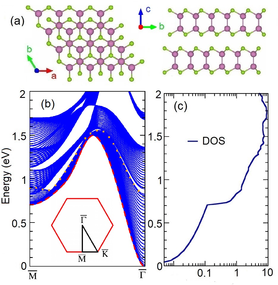
Single crystals of -InSe have been grown using the Bridgmann method from a non-stoichiometric melt Chevy . The crystallographic structure of -InSe is displayed inFig.1(a) (top and side views respectively left and right). Ultraviolet photoemission and photoluminescence spectra show that our bulk crystal is naturally n-doped and has direct band gap of 1.26 eV. We plot in Fig. 1(b) the calculated bulk band-structure projected on the surface plane, along the of the hexagonal Brillouin zone (BZ) (see inset). The dashed-red and dotted-orange lines point out the extension of the projected first conduction band. The correspondence between the bulk and surface BZ, a band structure along the complete path for a larger energy-range, as well as the technical details of the ab initio calculations are given in the supplementary file. We plot in Fig. 1(c) the projected density of electronic states calculated by Density Functional Theory (DFT), using ABINIT code Gonze , with lattice parameters from ref Magorrian , (see Supplemental supplemental ). As show by Fig. 1(c), the density of electronic states in the conduction band abruptly increases when the excess energy overcomes the bottom of the valley.
Our photon source is a Ti:Sapphire laser system delivering 6 J pulses with repetition rate of 250 kHz. Part of the fundamental beam ( eV) is converted to the second harmonic ( eV) in a -BBO crystal while the rest is employed to generate the third harmonic ( eV) and fourth harmonic beam ( eV) Faure . We photoexcite the sample either by the or pulses, generating carriers density of cm-3 and cm-3, respectively. The electrons emitted by the or pulse are discriminated in kinetic energy and angle with a resolution of 50 meV and degrees, respectively. Independently on the configuration of the experiment, the two beams generating the 2PPE signal display a cross correlation with FWHM ps. All samples have been cleaved at the base pressure of mbar and measured at temperature of 125 K.
Figure 2(a-d) shows the photoelectron intensity maps acquired along the direction at different delay time between the pulse and pulse. The image collected 1 ps before the arrival of the beam (Fig. 2(a)) is representative of the system in equilibrium conditions. According to the nominal -doping, we observe electrons in the conduction band minimun at excess energy eV. Two image-potential-states below are excited by the beam and are detected, at negative , by the pulse (Fig. 2(b,c)). Due to the short lifetime, the lowest image-potential-state is clearly visible only in the intensity map of Fig. 2(c). This map has been acquired at nominal value of zero delay and can be viewed as a snapshot of the primary excitations. Remark yet in Fig. 2(c) that the pulse populates the conduction band up to eV. The internal thermalization of such hot carriers proceeds faster than the cooling, probably because of an additional contribution of electron-electron scattering.
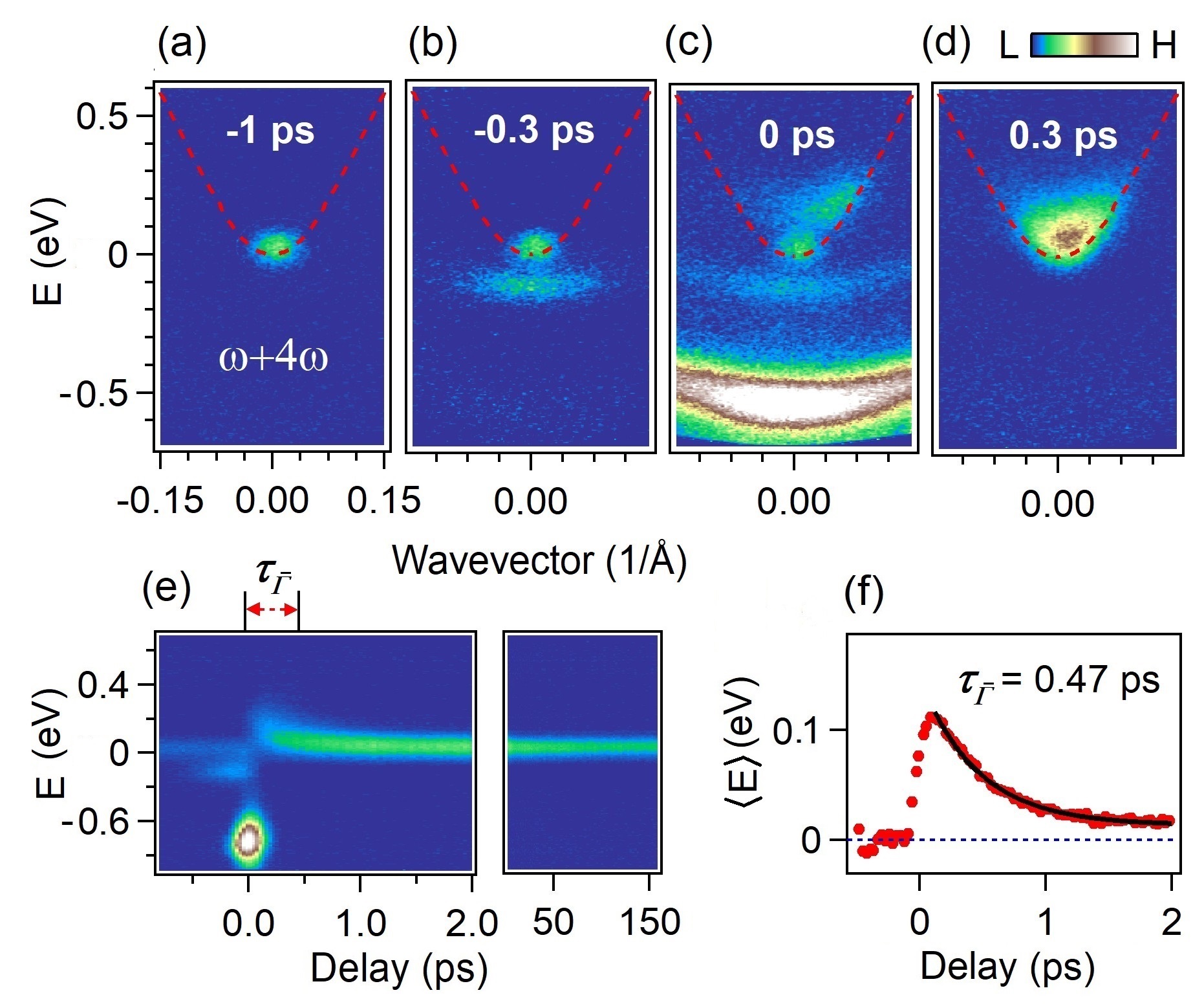
Figure 2(e) shows the photoelectron intensity integrated in the wavevector window [-0.1,0.1] Å-1 and plot as a function of pump probe delay. The average excess energy of the electrons in the conduction band is obtained by evaluating the integral in the interval eV. As shown by Fig. 2(f), the has intial value eV and it follows an exponential decay with time constant ps. This timescale elucidates the main relaxation mechanism of hot carriers in the valley. We recall that long-range Fröhlich interaction diverges in a material with three dimensional periodicity. Therefore, the polar optical coupling becomes the dominant electron-phonon scattering channel for small momentum transfer Jelena ; Tanimura2 .
Our calculations of vibrational properties and defomation potentials QuantumExpresso ; Jelena1 ; Jelena2 (see Supplemental supplemental ) confirm the important role of polar interaction in the intravalley cooling. We estimate the energy dissipation rate between 0.21 and 0.24 eV/ps at 125 K . Due to the long-range nature of the Frölich coupling, the phonon emission is weakly sensitive to the variation of electronic DOS. Therefore, is almost independent on as long as the excess energy is sufficiently larger than the phonon frequency. According to our theoretical estimate, hot carriers with an initial value eV require a characteristic time ps to approach the asymptotic level. The reasonably good agreement between and the experimental confirms that our simple analysis provides an accurate description of the observed cooling.
Next, we investigate the photoexcited state generated by pumping and probing the sample with and pulses, respectively. We mark in Fig. 3(a) the three indicative areas , and on the 2PPE intensity map. As shown in Fig. 3(b), the absorption of photons results in a rich variety of spectral features. The projected states of the conduction band span between the red dashed line and the orange dotted line that are superimposed to the intensity maps. This guideline is useful to discriminate between different processes leading to photoemitted electrons. On one hand, the strong and dispersing signal that is located in the projected band gap is due to direct 2PPE emission via virtual states (very strong in ). Such photoelectrons may mimic the initial state dispersion and become intense when propagating in emitted waves that match the boundary conditions. On the other hand, real intermediate states of the valley are excited by direct optical transitions from the , orbitals of the valence band. As in the case of GaAs, the efficient intervalley scattering can rapidly randomize the wavevector of electrons with high excess energy Tanimura1 ; Tanimura2 . This process sets in when overcomes the bottom of the valley at eV. By comparing Fig. 3(b) with Fig. 3(c), we deduce that electrons have already reached at ps (see evolution of the signal in ). Furthermore, the intervalley scattering steadily refills the states of the valley that are degenerate with (signal in ).
The dynamics of excited electrons can be tracked by focusing on selected regions in reciprocal space. We have integrated the 2PPE signal in the three indicative areas , and of Fig. 3(a). As shown by Fig. 3(e), the photoemission assisted by virtual states () follows the cross correlation between the pump and probe pulse. This signal has been employed to estimate the duration of optical pulses and to precisely determine zero delay. Note that states at the bottom of the valley () reach the highest occupation for ps. Although these electrons loose the initial momentum within few tens of femtoseconds, their energy dissipation is restrained by the low quantum energy of the emitted phonons. The most relevant modes that are involved in the scattering process are acoustic branches close to the zone boundary and with typical energy of meV. Our calculations indicate that electrons with eV scatter with such phonons on an average timescale of 8 fs at 125 K. The energy dissipation time at high excess energies is mostly determined by short-wavelength phonon scattering, which depends strongly on the excess energy. According to our theoretical estimates the electrons that are at 0.5 eV above require a characteristic time constant of 0.2 ps to reach the bottom of the valley (see Supplemental supplemental ).
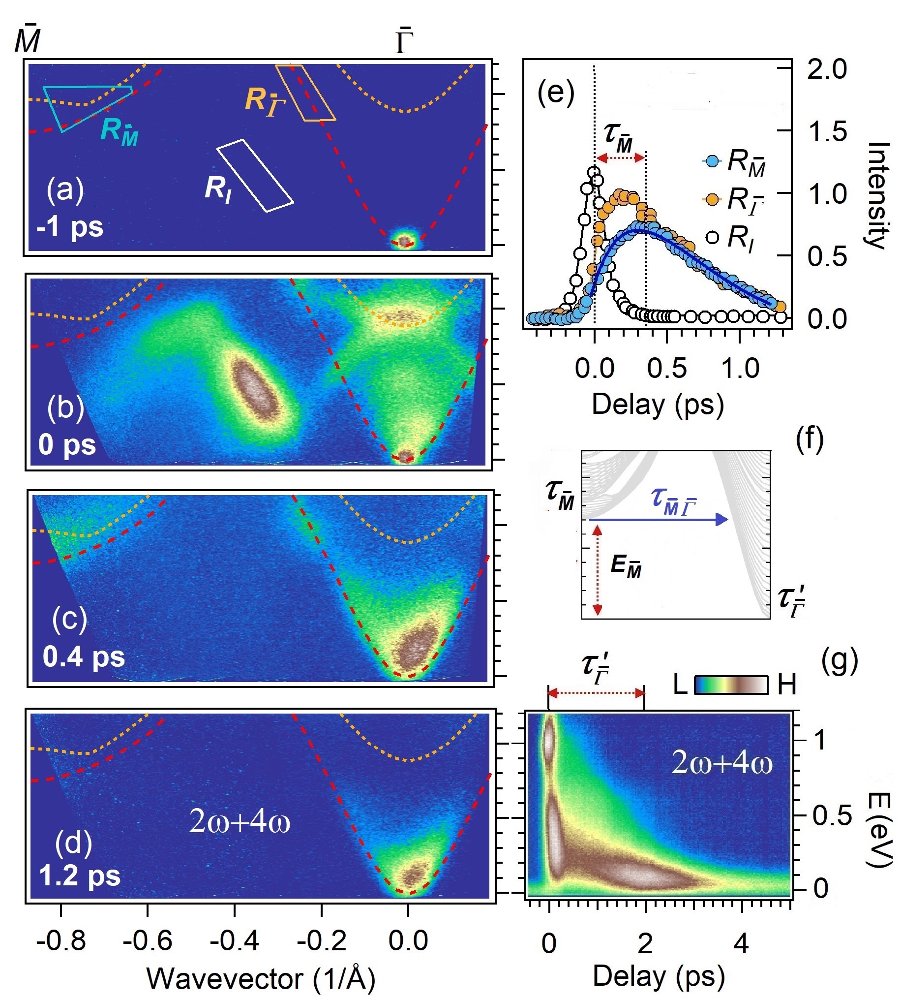
Figure 3(e) shows also that electrons in the valley and electrons in the valley display an identical dynamics for . These nearly-degenerate states are maintained in detailed balance conditions by phonons with wavevector near to the point. The transition time calculated at 125 K is fs and it turns out to be short enough to confirm our conjecture. Eventually, the large eV may suggest that 180 fs (or 80 fs at 300 K) is surprisingly long. This result does not derive from unconventional matrix elements of electron-phonon coupling but rather from the small DOS of the valley at (See Fig. 1(c)). We find instructive the comparison of InSe with other chalcogenides: electrons that are resonantly excited at 300 K in the valley of bulk MoS2 Wallauer or WSe2 Bertoni require fs to reach the valley and the energy separation between and valley is only eV. In the case of InSe, the excess energy is particularly large and therefore the carriers can be sustained above the conduction band minimum for long time. Moreover, the abrupt increase of the DOS for eV, can boost the injection of electrons in the valley. Once these electrons fall below , the intervalley scattering is no longer active whereas the cooling proceeds mainly via Fröoling coupling to phonons with small momentum transfer Tanimura1 ; Tanimura2 . Figure 3(g) shows the photoelectron signal integrated around the valley in a wavevector window of [-0.25, 0.25] Å-1. The maximal carrier density at the bottom of the conduction band is achieved ps after photoexcitation.
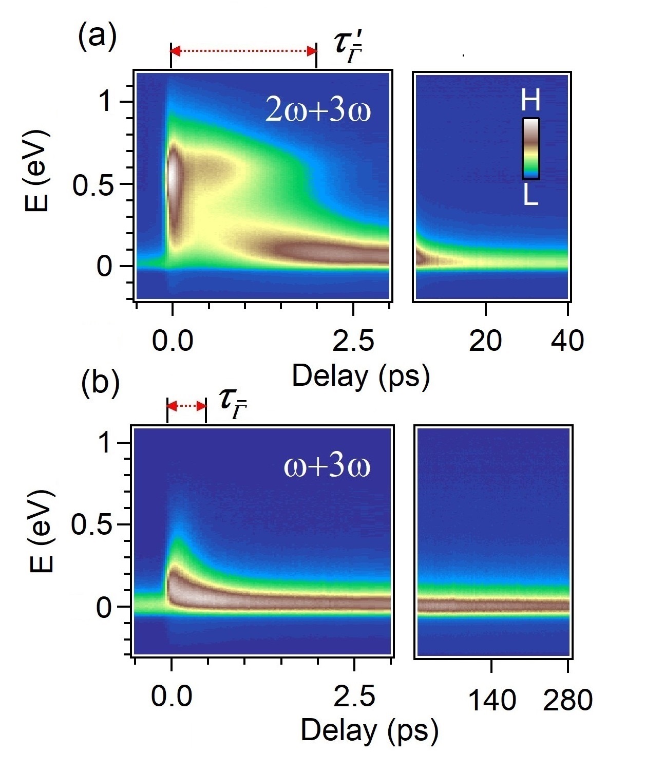
Figure 4(a) and Fig. 4(b) display the 2PPE signal probed in the valley by 3 photons and excited with 2 and , respectively. Being independent on the DOS, the Frölich dissipation rate is the same in both cases. However, the electrons hailing from the valley gather in the valley near to the calculated . As a consequence, the energy dissipation takes much longer in Fig. 4(a) than in Fig. 4(b). By assuming that intervalley scattering generate an average kinetic energy eV, the resulting cooling time ps is consistent with the observed .
Next, we estimate the minimal distance at which two electrodes should be placed in order to extract the hot carriers. The effective mobility cm2V-1s-1 is given by the model for linear dispersion Avouris at 0.7 eV excess energy and 125 K (see Supplemental supplemental ). Due to the high excess energy of hot electrons, the nominal is lower than the mobility measured in InSe transistors Bandurin . Nonetheless a driven drift can still attain high values. Upon an applied voltage of Volts, the hot electrons reach the electrodes if .
The relatively large distance that can be covered by hot carriers suggests original concepts for optoelectronic applications. Recently Lao et al. developed a long-wavelength photodetection principle working far from equilibrium conditions Lao . Hot carriers injected into -doped GaAs structure interact with cold carriers and promote them to states of high excess energy. The tunneling of such holes through AlxGa1–xAs barriers enables a long-wavelength infrared response that can be tuned via the applied voltage. By direct analogy, the hot electrons in the valley of InSe could extend such promising approach to chalcogenides heterostructures.
A second possible application of hot carriers generation are Gunn diodes. In III/V semiconductors, a microwave signal of high frequency appears if the applied bias field exceeds a threshold value Butcher . This effect arises when the high electrical field promotes electrons from the conduction band minimum to an upper valley Butcher ; McCumber . As a consequence the average mobility of electrons decreases, while the device enters in a regime of negative differential resistance. The heavy mass of valley should favor this process also in InSe. If confirmed, our conjecture may lead to the development of microwave oscillators and bistable switches based on chalcogeniges materials.
In conclusion, we have shown that InSe has excellent potential for hot carrier optoelectronics. The high energy density of electronic states above the bottom of valley favors the photoassisted or electrical injection of electrons with high excess energy. On the other hand, electrons that reached the valley can dissipate energy only via Fröhlich coupling to optical phonons. These hot carriers have typical lifetime of 2 picoseconds and could be extracted from a device of micron. We could successfully model the observed dynamics by first principle calculations of the electron-phonon scattering. Our results will be of guidance for the physics of electron-phonon coupling in other layered chalcogenides. Moreover, we suggest appealing concepts, such as below band-gap photodetection or negative differential resistance, that could be shortly integrated in to the family of van der Waals semiconductors.
We thanks DIM-Oximore and the Ecole Polytechnique for funding under the project ’ECOGAN’. This work was supported by LABEX PALM (ANR-10-LABX-0039-PALM, Project Femtonic) and by the EU/FP7 under the contract Go Fast (Grant No. 280555). Computer time has been granted by GENCI (project 2210) and by Ecole Polytechnique through the LLR-LSI project.
References
- (1) K. F. Mak, C. Lee, J. Hone, J. Shan, and T. F. Heinz, Phys. Rev. Lett. 105, 136805 (2010).
- (2) V. Tran, R. Soklaski, Y. Liang, and L. Yang, Phys. Rev. B 89, 235319 (2014).
- (3) Garry W. Mudd Simon A. Svatek, Tianhang Ren, Amalia Patané Oleg Makarovsky, Laurence Eaves, Peter H. Beton, Zakhar D. Kovalyuk, George V. Lashkarev, Zakhar R. Kudrynskyi and Alexandr I. Dmitriev, Adv. Mater. 25, 5714 (2013).
- (4) K. F. Mak, K. He, J. Shan, and T. F. Heinz, Nat. Nanotechnol. 7, 494 (2012).
- (5) B. Radisavljevic, A. Radenovic, J. Brivio, V. Giacometti, and A. Kis, Nat. Nanotechnol. 6, 147 (2011).
- (6) L. Li, Y. Yu, G. J. Ye, Q. Ge, X. Ou, H. Wu, D. Feng, X. H. Chen, and Y. Zhang, Nat. Nanotechnol. 9, 372 (2014).
- (7) Denis A. Bandurin, Anastasia V. Tyurnina, Geliang L. Yu, Artem Mishchenko, Viktor Zólyomi, Sergey V. Morozov, Roshan Krishna Kumar, Roman V. Gorbachev, Zakhar R. Kudrynskyi, Sergio Pezzini, Zakhar D. Kovalyuk, Uli Zeitler, Konstantin S. Novoselov, Amalia Patanè, Laurence Eaves, Irina V. Grigorieva, Vladimir I. Fal’ko, Andre K. Geim and Yang Cao, Nat. Nanotechnol. 12, 223 (2017).
- (8) K. I. Bolotin, K. J. Sikes, Z. Jiang, M. Klima, G. Fudenberg, J. Hone, P. Kim, and H. L. Stormera, Solid State Commun. 146, 351 (2008).
- (9) C. R. Dean, A. F. Young, I. Meric, C. Lee, L. Wang, S. Sorgenfrei, K. Watanabe, T. Taniguchi, P. Kim, K. L. Shepard and J. Hone, Nature Nanotechnol. 5, 722 (2010).
- (10) Sidong Lei, Liehui Ge, Sina Najmaei, Antony George, Rajesh Kappera, Jun Lou, Manish Chhowalla, Hisato Yamaguchi, Gautam Gupta, Robert Vajtai, Aditya D. Mohite, and Pulickel M. Ajayan, ACS Nano 8, 1263 (2014).
- (11) Srinivasa Reddy Tamalampudi, Yi-Ying Lu, Rajesh U. Kumar, Raman Sankar, Chun-Da Liao, Karukanara B. Moorthy, Che-Hsuan Cheng, Fang Cheng Chou, and Yit-Tsong Chen, Nano Lett. 14, 2800 (2014).
- (12) Z. Chen, J. Biscarasa, and A. Shukla, Nanoscale 7, 5981 (2015).
- (13) Wenshan Zheng, Tian Xie, Yu Zhou, Y. L. Chen, Wei Jiang, Shuli Zhao, Jinxiong Wu, Yumei Jing, Yue Wu, Guanchu Chen, Yunfan Guo, Jianbo Yin, Shaoyun Huang, H. Q. Xu, Zhongfan Liu and Hailin Peng, Nat. Commun. 6, 6972 (2015).
- (14) Sidong Lei, Fangfang Wen, Liehui Ge, Sina Najmaei, Antony George, Yongji Gong, Weilu Gao, Zehua Jin, Bo Li, Jun Lou, Junichiro Kono, Robert Vajtai, Pulickel Ajayan, and Naomi J. Halas, Nano Lett. 15, 3048 (2015).
- (15) S. Nüsse, P. H. Bolivar, H. Kurz, F. Levy, A. Chevy, and O. Lang, Phys. Rev. B 55, 4620 (1997).
- (16) P. Dey, J. Paul, N. Glikin, Z. D. Kovalyuk, Z. R. Kudrynskyi, A. H. Romero, and D. Karaiskaj, Phys. Rev. B 89, 125128 (2014).
- (17) Y.Ohtsubo, J. Mauchain, J. Faure, E. Papalazarou, M. Marsi, P. Le Fèvre, F. Bertran, A. Taleb-Ibrahimi and L. Perfetti, Phys. Rev. Lett. 109, 226404 (2012).
- (18) A. G. Cabo, J. A. Miwa, S. S. Gronborg, J. M. Riley, J. C. Johannsen, C. Cacho, O. Alexander, R. T. Chapman, E. Springate, M. Grioni, J. V. Lauritsen, P. D. C. King, P. Hofmann and S. Ulstrup, Nano Lett. 15, 5883 (2015).
- (19) A. Chevy, J. Cryst. Growth 67, 119 (1984).
- (20) X. Gonze, B. Amadon, P.-M. Anglade, J.-M. Beuken, F. Bottin, P. Boulanger, F. Bruneval, D. Caliste, R. Caracas, M. Côté, et al., Computer Phys. Commun. 180, 2582 (2009).
- (21) S. J. Magorrian, V. Zòlyomi, and V. I. Fal’ko, Phys. Rev. B 94, 245431 (2016).
- (22) See Supplemental Material at [] for details on the theoretical calculations.
- (23) J. Faure, J. Mauchain, E. Papalazarou, W. Yan, J. Pinon, M. Marsi, and L. Perfetti, Rev. Sci. Instrum. 83, 043109 (2012).
- (24) J. Sjakste, N. Vast, M. Calandra and F. Mauri, Phys. Rev. B 92, 054307 (2015).
- (25) H. Tanimura, J. Kanasaki, K. Tanimura, J. Sjakste, N. Vast, M. Calandra, and F. Mauri, Phys. Rev. B 93, 161203(R) (2016).
- (26) P. Giannozzi, O. Andreussi, T. Brumme, O. Bunau, M. B. Nardelli, M. Calandra, R. Car, C. Cavazzoni, D. Ceresoli, M. Cococcioni, et al., J. Phys.: Condens. Matter 29, 465901 (2017), URL http://www.quantum-espresso.org.
- (27) J. Sjakste, N. Vast, and V. Tyuterev, Phys. Rev. Lett. 99, 236405 (2007).
- (28) V. G. Tyuterev, S. V. Obukhov, N. Vast, and J. Sjakste, Phys. Rev. B 84, 035201 (2011).
- (29) J. Kanasaki, H. Tanimura, and K. Tanimura, Phys. Rev. Lett. 113, 237401 (2014).
- (30) R. Wallauer, J. Reimann, N. Armbrust, J. Güdde, and U. Höfer, Appl. Phys. Lett. 109, 162102 (2016).
- (31) R. Bertoni, C. W. Nicholson, L. Waldecker, H. Hübener, C. Monney, U. De Giovannini, M. Puppin, M. Hoesch, E. Springate, R. T. Chapman, C. Cacho, M. Wolf, A. Rubio, and R. Ernstorfer, Phys. Rev. Lett. 117, 277201 (2016).
- (32) W. Zhu, V. Perebeinos, M. Freitag, and P. Avouris, Phys. Rev. B 80, 235402 (2009).
- (33) Y. F. Lao, A. G. U. Perera, L. H. Li, S. P. Khanna, E. H. Linfield, and H. C. Liu, Nature Photon. 8, 412 (2014).
- (34) Butcher, P. N., Reports on Progress in Physics 30, 97 (1967).
- (35) McCumber, D. E. and Chynoweth, A. G., IEEE Transactions on Electron Devices 13, 4 (1966).