Compact ultracold electron source based on a grating magneto-optical trap
Abstract
The ultrafast and ultracold electron source, based on near-threshold photoionisation of a laser-cooled and trapped atomic gas, offers a unique combination of low transverse beam emittance and high bunch charge. Its use is however still limited because of the required cold-atom laser-cooling techniques. Here we present a compact ultracold electron source based on a grating magneto-optical trap (GMOT), which only requires one trapping laser beam that passes through a transparent accelerator module. This makes the technique more widely accessible and increases its applicability. We show the GMOT can be operated with a hole in the center of the grating and with large electric fields applied across the trapping region, which is required for extracting electron bunches. The calculated values of the applied electric field were found to agree well with measured Stark shifts of the laser cooling transition. The electron beams extracted from the GMOT have been characterised. Beam energies up to were measured using a time-of-flight method. The normalised root-mean-squared transverse beam emittance was determined using a waist scan method, resulting in . The root-mean-squared transverse size of the ionisation volume is or larger, implying an electron source temperature in the few- range, orders of magnitude lower than conventional electron sources, based on photoemission or thermionic emission from solid state surfaces.
pacs:
37.10, 37.20, 41.75, 41.85I Introduction
In the past decade new tools have emerged that allow investigation of structural dynamics with atomic spatial and temporal resolution, i.e. as small as and : Ultrafast Electron MicroscopyZewail (2010); Flannigan and Zewail (2012); Baum, Yang, and Zewail (2007); King et al. (2005) (UEM), Ultrafast Electron DiffractionHastings et al. (2006); Siwick et al. (2003); Musumeci et al. (2010); Shen et al. (2018) (UED) and X-ray crystallography using Free Electron Lasers (XFELs)Chapman et al. (2011); Boutet et al. (2012); Kang et al. (2015). This revolution would not have been possible without the spectacular development of ultrafast pulsed electron sourcesAkre et al. (2008). By femtosecond photoemission from flat photocathodes in RF photoguns, highly charged electron bunches can be created of sufficient quality to drive XFELs, enabling single-shot, femtosecond X-ray diffraction of protein nanocrystals Chapman et al. (2011). Unfortunately XFELs are big and costly facilities with limited access for the average researcher. In an alternative approach the electron bunches that drive the XFELs can also be directly used for single-shot UED Hastings et al. (2006); Li et al. (2011); Shen et al. (2018).
Using electrons instead of X-rays has the great advantage of smaller, cheaper setups. However, the beam quality is not sufficient for studying complicated macromolecular structures or for imaging with (sub)nanometer resolution. Higher beam quality is generally provided by sharp-tipped sources, developed for electron microscopy. By sideways femtosecond photoemission from a nanometer-sized field emission tip Feist et al. (2017) (or by RF chopping Oldfield (1976); Verhoeven et al. (2018); van Rens et al. (2018)) the same beam quality can be achieved as in conventional electron microscopy, enabling imaging with atomic spatial and temporal resolution. However, this results on average in less than one electron per pulse. Increasing the charge per pulse spoils the beam quality and therefore the atomic resolution. A source that offers the combination of high beam quality and high bunch charge is highly desirable.
In the quest for better beam coherence while maintaining a large source size, a new electron source was proposed Claessens et al. (2005), the ultracold electron source (UCES). In the UCES the initial transverse angular momentum spread is decreased which results in increased beam coherence for a given source size Engelen et al. (2013, 2014); McCulloch et al. (2013). This significantly reduces Coulomb effects at the source which allows extraction of more charge, required for single-shot measurements.
In the UCES high charge electron bunches are created by near threshold photo-ionisation of a cloud of laser-cooled and trapped atoms in a magneto optical trap (MOT) Metcalf and van der Straten (2001). Previous work showed high quality diffraction patterns van Mourik et al. (2014); Speirs et al. (2015) with these bunches, demonstrating pulsed electron source temperatures as low Engelen et al. (2013); McCulloch et al. (2013); Engelen et al. (2014) as a few-. Additionally it was shown that it is possible to extract ultracold picosecond electron pulses Franssen et al. (2017) which can in principle be compressed to using well established RF compression techniques van Oudheusden et al. (2010).
In this work we present a novel compact ultracold electron source based on a grating magneto-optical trap (GMOT), which only requires one trapping laser beam. This makes the technique more widely accessible and therefore increases its applicability. The paper is organised as follows: In Section II we describe the operating principle of a GMOT. Next, in Section III, we discuss the design of the ultracold electron source, the vacuum system, the accelerator and the electron beamline. In Section IV we will show that it is possible to operate a GMOT with a hole in the center of the grating and with large electric fields applied across the trapping region, which are both required for extracting electron bunches. We will also show that the calculated values of the applied electric field agree well with measured Stark shifts of the laser cooling transition. Finally, in section V we will discuss the commissioning of the ultracold electron source. The electron beams extracted from the GMOT have been characterised. Beam energies up to were measured using a time-of-flight method. The normalised root-mean-squared (rms) transverse beam emittance was determined using a waist scan method, resulting in . The rms transverse source size is or larger, implying an electron source temperature less than .
II The principle of a grating MOT based UCES
In a conventional magneto-optical trap (MOT) atoms are laser cooled using three pairs of orthogonal laser beams whose frequency is red shifted with respect to the atomic laser cooling transition. The atoms are trapped using a quadrupole magnetic field which creates position-dependent resonance conditionsMetcalf and van der Straten (2001) for the atomic transition through the Zeeman effect, and thus a restoring force and stable trapping. A recent development in the field of laser cooling and trapping is the Grating MOTNshii et al. (2013) which requires only one input laser beam instead of the six for a conventional MOT.
II.1 Grating MOT
The GMOT, developed at University of Strathclyde, Glasgow, is based on an optical grating that diffracts a single incoming circularly polarised laser beam. The MOT is formed inside the overlap volume which is spanned by the incoming beam, the zeroth order back reflection and three first order diffracted beamsMcGilligan et al. (2017, 2016); Nshii et al. (2013); Cotter et al. (2016). The grating chip consists of three identical linear gratings, lying in a plane with relative orientations, see Figure 1a). Each grating diffracts the incoming laser beam according to Bragg’s law,
| (1) |
with the grating period, () the diffraction order and nm the Rubidium trapping laser wavelength. We have used two gratings with periods and which result in first order diffraction angles and respectively. The diffraction angle is defined as the angle between the grating normal and the diffracted beam, see Figure 1d and e. Figure 1b shows a scanning electron microscope (SEM) image of the grating structure at a position where two gratings meet. Higher diffraction orders () are cut off because . The radial force balanceMcGilligan et al. (2016) for both gratings is automatic when the incoming beam is aligned with the center of the grating.
The chip measures while the chip measures . Both chips are manufactured in silicon and have a nm top layer of aluminium which reflects the incoming laser beam. The gratings are fabricated using electron beam lithography and have a duty cycle and a nm etch depthNshii et al. (2013).
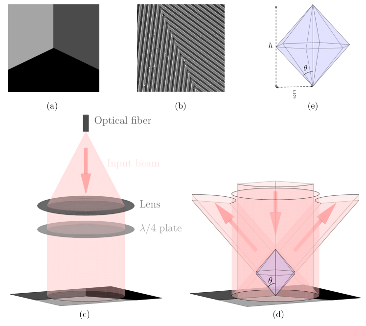
Figure 1c shows a single linearly polarised laser beam emanating from an optical fiber, which is collimated using a lens and subsequently circularly polarised using a quarter wave plate. Figure 1d shows that when the center of the beam is aligned with the center of the grating three first order diffracted beams are created which span the overlap volume (purple). The overlap volume approximately has the shape of a double hexagonal pyramid as is shown in Figure 1e. The height of the overlap volume is with the rms radius of the laser beam. The experiments using the chip have been done with a Gaussian input laser beam with a beam radius of . The experiments using the chip were done with a flattop input beam with a radius . Using these values we calculate and . The cold gas can be trapped anywhere inside the overlap volume. The exact position of the atom cloud is determined by the zero point of the magnetic quadrupole field. The () trap volume is given by
| (2) |
With the above mentioned beam parameters we calculate the overlap volume and . The atom number scalesLindquist, Stephens, and Wieman (1992) with the overlap volume according to . The Riis group have reportedNshii et al. (2013) that it is possible to trap atoms using a grating MOT with an overlap volume of . Using the scaling law we expect to be able to trap and atoms in our experiment.
II.2 Ultracold electron source
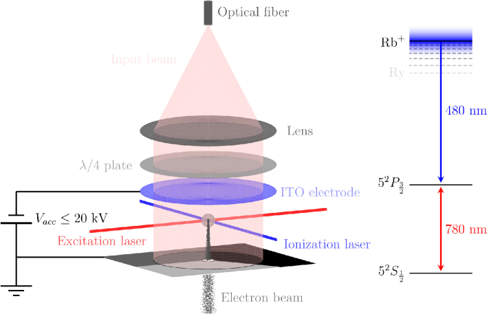
Figure 2 shows a schematic representation of the electron gun. First the MOT is loaded with -rubidium atoms, then the trapping beam is switched off for a few so that all atoms relax back to the ground state. During these few a small cylinder ( waist) of atoms is excited using a cw excitation laser beam (). The excitation laser beam is intersected by a pulsed ionisation laser beam at right angles which is focused down to a waist. This results in an approximately Gaussian spherical ionization volume with a root-mean-square (rms) radius . The wavelength of the ionisation laser is tuned close to the ionisation threshold to minimise the excess energy gained by the electron. The Stark shifted excess energy is given by
| (3) |
with the zero-field ionization laser wavelength threshold, the Hartee energy, the applied electric field across the MOT, the atomic unit of electric field, plank’s constant and the speed of light. Ultracold electron bunches have been generated by using nanosecond ionization laser pulses Claessens et al. (2007); Taban et al. (2010) and later by femtosecond pulses Engelen et al. (2013); McCulloch et al. (2013). The length of the ionization volume determines the energy spreadFranssen et al. (2017, 2018) of the electron beam. Additionally, the initial electron distribution can be tailoredMcCulloch et al. (2011) in 3D by shaping of the ionisation and excitation laser beams.
To extract an electron beam a static electric field is applied across the trapped cloud of atoms. The negative electrode is an Indium-Tin-Oxide (ITO) coated quartz disk that is transparent for the trapping laser beam; the grounded grating chip is the positive electrode, which has a hole in the center, allowing the electron beam to pass through. The distance of the ionisation volume to the grating combined with the applied voltage determine the amount of energy the electron beam acquires.
III Detailed experimental Design
We have designed a modular compact turn-key ultracold electron source that offers maximum optical accessibility. To keep the design simple we decided to have both the MOT coils and the high-voltage (HV) outside the vacuum, avoiding vacuum feed-throughs. A breakout cross-section of the vacuum system is depicted in Figure 3. The main body of the electron gun consists of a CF100 cube. The left flange is a re-entrant flange which allows the accelerator module to be mounted close to the grating. The grating is embedded in a holder which is connected to the re-entrant flange.
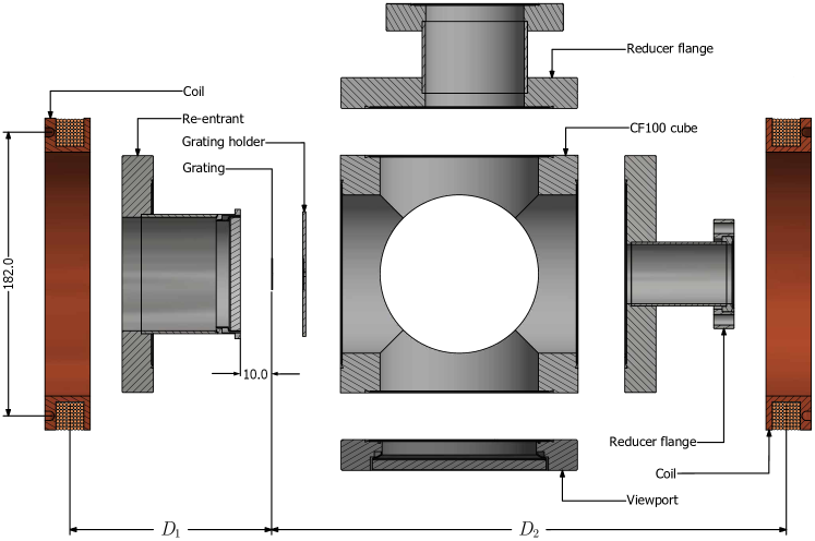
The right flange is a reducer flange which couples the cube to the electron beamline. The bottom, front and back of the cube are sealed with CF100 UV grade viewports. The top flange is a CF100 to CF63 reducer which houses the rubidium dispensers providing a rubidium background pressure of mbar. The base pressure of the vacuum system is mbar. The two coils generate the magnetic quadrupole field that is required to trap the rubidium atoms.
III.1 Quadrupole field
The magnetic field coils are asymmetrically driven to compensate for the fact that the trapped gas cloud is not in the center of the CF100 cube (), see Figure 3. Due to the large coil radius and the large distance from the coils to the trapped gas we need Ampere turns to provide the desired axial magnetic field gradient of . Both coils have turns and a radius . The distance from the first coil to the grating surface is and the distance from the second coil to the grating surface . The distance between the gas cloud and the grating surface determines the ratio between the coil currents:
| (4) |
with and the currents running through the first coil and second coil, respectively. Typically we operate the coils at A and A. This results in an axial gradient . The position of the gas cloud inside the overlap volume can be controlled by changing the current running through either one of the coils. Typically the MOT is formed in the center of the overlap volume which means that or depending on the grating that is used, see Section II.1.
III.2 Accelerator
To reach electron energies of we need an electric field strength of across a gap. To avoid HV feedthroughs we designed a HV module which is mounted outside the vacuum, inspired by ReferenceGunton et al. (2016). The accelerator module can be inserted into the re-entrant flange, see Figure 3. The electrode is an Indium Tin Oxide (ITO) coated quartz plate and therefore transparent for nm light. Figure 4 shows a cross-sectional view of the accelerator module.
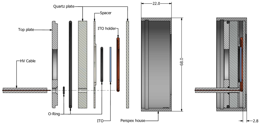
The accelerator house is made from perspex, the bottom layer is a quartz disk. On top of this disk we glued a copper ring (ITO holder) which is connected to a high voltage power supply. The ITO plate is glued onto the copper ring with conductive epoxy, electrically connecting the copper and the ITO surface. On top of the ITO plate we have an O-ring and a spacer holding it in place. On top of this we have another quartz plate and a top plate which is used to compress all the O-rings to make sure that the cavities are sealed. The volume in the assembly between the two quartz plates but outside the O-ring is filled with epoxy. In this way the HV electrode is shielded from the environment with a high dielectric constant material, while keeping the compartments where the trapping laser passes through free from epoxy.
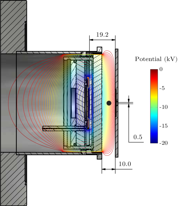
Figure 5 shows a cross-sectional view of the accelerator module mounted in the re-entrant flange, which is pushed against the viewport using a styrofoam spacer. The high voltage electrode and the grounded grating support are separated by . The figure also shows the equipotential lines of the acceleration field with the electrode at . The gas cloud (indicated by the black dot) is trapped in between the viewport and the grating, which are separated by of vacuum. The accelerated electrons pass through a hole in the grating with a diameter of . Figure 6 shows an image of the grating with the hole in the center (left) and a closeup SEM image of the hole (right).

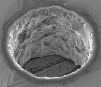
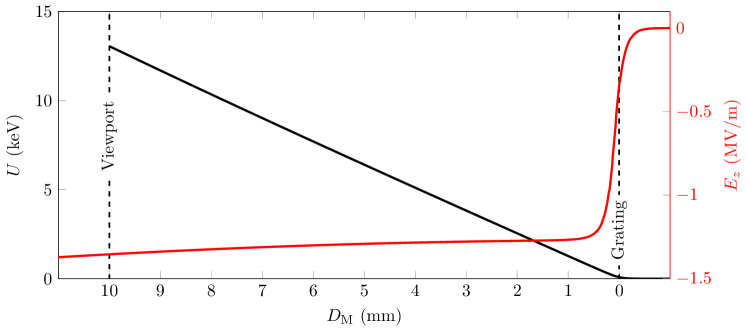
Figure 7 shows the simulated electric field and the final electron kinetic energy reached as a function of distance between the gas cloud and the grating for an accelerator potential . The further away the electrons are created from the grating the larger the final kinetic energy . Based on the height of the overlap volume we expect to create at MOT at or depending on the grating that is used, see Section II.1. This would result in an electron beam energy for the chip and for the chip.
III.3 Beamline
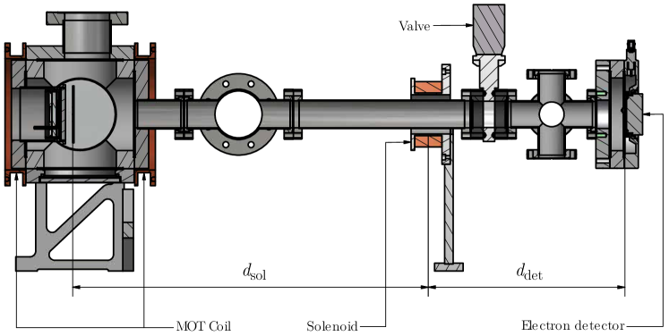
Figure 8 shows a cross-sectional view of the electron gun and beamline. The electrons are created in the vacuum space between the re-entrant and the grating support, see Figure 5 for a more detailed view. The divergence and size of the electron beam can be controlled by the magnetic solenoid lens positioned at a distance from the gas cloud. The detector assembly is positioned behind the magnetic solenoid lens. The detector assembly consists of a micro-channel plate (MCP) and a phosphor screen which is imaged onto a CCD camera.
IV Commissioning Grating MOT
We have tested the operation of the GMOT under the influence of an applied electric field and with a hole in the center of the grating chip. The measurements were done using the grating chip. The input laser beam has at the trapping wavelength and at the repump wavelength. The trapping beam has a beam diameter of resulting in a trapping beam peak intensity , which is well above the rubidium saturation intensity Metcalf and van der Straten (2001). The repump beam peak intensity is . The atom numbers were estimated using fluorescence measurements with a saturated atomic scattering rate .
Typically atoms can be loaded in , corresponding to a loading rate . This implies that the loading rate is sufficient to extract electron bunches containing on the order of electrons per pulse at a repetition rate of . The peak atom density is reached for a magnetic field gradient .
IV.1 DC Stark shift
The detuning at which the number of atoms in the trap is maximal changes if an electric field is applied due to Stark shifting of the cooling transition frequency. The energy levels for the hyperfine states of the ground state -rubidium atom all shift equally Krenn et al. (1997). The excited state energy levels are shifted differently depending on the hyperfine state due to a non-zero tensor polarisabilityKrenn et al. (1997).
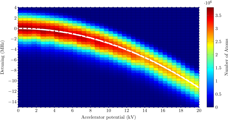
Figure 9 shows the number of atoms in the trap as a function of accelerator potential and detuning with respect to the optimal detuning when no electric field () is applied. The white line shows the calculated Stark shift, for the transition to for final . We assumed the Stark shift to be small compared to the hyperfine splittingsKrenn et al. (1997) which holds for . The white curve corresponds to an electric field at the position of the gas cloud. This agrees well with the simulated electric field strength at a position for an accelerator potential of , shown in Figure 7.
Figure 9 also shows that the number of atoms in the trap decreases as the electric field is increased. This is due to broadening of the laser cooling transition by breaking of the degeneracy of the levels in the stateGunton et al. (2016). At maximum electric field we still have a steady state atom number which is more than sufficient to operate the GMOT as an electron source.
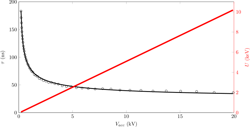
V Commissioning UCES
In the previous section we showed that atoms are trapped in the presence of a acceleration field using the grating chip. The MOT was ionised using a tuneable nanosecond ionisation laser pulse with a rms pulse duration of . The electron beam energy was measured by an electron time-of-flight scanEngelen et al. (2014) which resulted in a modest electron beam energy . This is also what we expect on the basis of the position of the gas cloud for the grating chip, see Section III.2. We decided to replace the diffraction grating by a grating which allowed us to create the gas cloud above the grating surface, as expected from the height of the overlap volume. Additionally, this also increases the overlap volume which results in a gas cloud containing atoms. The larger value of increased the maximum achievable electron beam energy to . The input laser beam has a circular (diameter of ) flattop intensity distribution with and .
In this section we present measurements of the electron beam energy, using a time-of-flight method, and of the transverse beam quality using a waist scanEngelen et al. (2013, 2014) method.
V.1 Time-of-Flight
The electron beam energy was determined using an electron time-of-flight (TOF) scanEngelen et al. (2014). The arrival time of the electron pulse on the MCP was determined by measuring the charge signal with a trans-impedance amplifier. Figure 10 shows the arrival time of the electron pulse relative to the ionisation time as a function of acceleration voltage .
The resulting TOF data was fit, solid line in Figure 10, using the relativistically correct expression
| (5) |
with the speed of light, the electron mass, an accelerator potential offset and an electronics delay. This function was fitted with , and as fitting parameters, yielding , and . The electron energy is given by
| (6) |
with the electron charge. The final electron beam energy as a function of accelerator voltage calculated using Equation 6 is shown in Figure 10. The maximum achievable electron energy is for an accelerator potential .
During operation, the re-entrant viewport gets coated with a thin layer of rubidium which reduces the work function of the quartz surface. Scattered ionisation laser photons give rise to photoemission which charges the glass plate, effectively creating a voltage offset . Carefully aligning the ionisation laser and taking measure to prevent scattering of the laser light minimises the charging. Alternatively the viewport can be heated.
Additionally, the rubidium ions are accelerated towards the quartz plate. These ions can produce electrons by ion impact ionisation if they acquire sufficient kinetic energy. This causes a second electron signal on the electron detector which arrives about later than the electrons extracted from the Rubidium atoms. Switching the accelerator voltage off when the electrons have passed the grating should reduce the ion kinetic energy and thus the secondary electron yield. Alternatively, immediately switching the polarity of the field after the electrons have passed the grating will further decelerate the ions.
V.2 Beam quality
The transverse electron beam quality is given by the normalized rms transverse emittance which is defined by
| (7) |
with the transverse position coordinate with respect to the bunch center and the transverse momentum with respect to the average transverse bunch momentum. The brackets denote averaging over the electrons in the bunch. The beam emittance is fixed at the source. Here the position and momentum coordinate are uncorrelated, i.e. , and therefore the emittance is equal to the product of beam size and uncorrelated transverse momentum spread . The transverse size of the electron beam at the source was determined to be by measuring the spot size of the excitation laser beam in a virtual source point. The normalized beam emittance is related to the source temperature by
| (8) |
where we used with the Boltzmann constant. The normalised emittance can be determined from a waistscanEngelen et al. (2013, 2014). In a waist scan the size of the electron beam on the detector is measured as a function of focusing power of a magnetic solenoid lens. The ionisation laser wavelength was tuned to so that the electrons only receive a small amount of excess energy. At an electric field strength this results in which should result in ultracold electron bunchesEngelen et al. (2013, 2014); McCulloch et al. (2013).
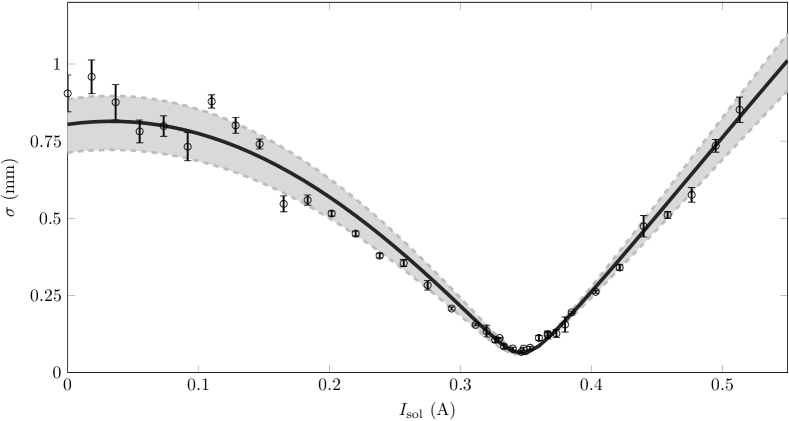
Figure 11 shows the rms transverse beam size as measured on the detector as a function of current running through the solenoid. At the focus an rms electron spot size was reached which is at the limit of our detector resolution. Detailed charged particle tracking simulations were done, in which the source temperature was varied while the source size was kept fixed. We used realistic fields for the accelerating field, the quadrupole magnetic field of the MOT coils and the field produced by the magnetic solenoid lens. Coulomb interactions can be neglectedFranssen et al. (2017) because we have used a nanosecond ionization laser pulse. The measured data was fitted with the simulation resultsEngelen et al. (2014) which was quadratically added to the detector resolution. The solid black line in figure 11 is the best fit with particle tracing simulations.
The fit results in a beam emittance , which corresponds to a source temperature . The grey band in the figure defines an upper and a lower limit (dashed lines) for the source emittance. At the lower limit this results in and at the upper limit . Using , this translates into a lower temperature limit and an upper temperature limit . The inner data points (close to the focus) imply a source temperature even lower than . The measured source temperature and beam emittance of the GMOT UCES are in line with results reported in earlier work Engelen et al. (2013, 2014); McCulloch et al. (2013).
VI Conclusion and outlook
We have successfully developed a compact ultracold electron source based on a GMOT. The unique modular design only requires one input beam that passes through a transparent accelerator module. We show that the GMOT can be operated with a hole in the center of the grating and with large electric fields applied across the trapping region. The electric field was determined by measuring the Stark shifts of the laser cooling transition.
The electron beams extracted from the GMOT have been characterised. Beam energies up to were measured using a time-of-flight method. The normalised root-mean-squared transverse beam emittance was determined using a waist scan method, resulting in . Since the root-mean-squared transverse size of the ionisation volume is or larger, this implies an electron source temperature in the range.
We have demonstrated a clear path towards harnessing the great potential of the UCES in a practical setting. Future research will focus on increasing the bunch charge of picosecond electron pulses created by femtosecond photoionisation. These pulses are sufficiently short for RF acceleration and compression, creating intriguing new possibilities. Obviously space charge forces will become a problem at higher bunch charges which can be addressed by shaping of the initial electron distribution.
Acknowledgements.
We acknowledge valuable discussions with A. Arnold, E. Riis, P. Griffin, J. McGilligan and J. Conway. The grating was supplied by the Strathclyde grating MOT team. The hole in the grating was drilled by Tiny den Dekker from Philips innovation services. This research is supported by the Institute of Complex Molecular Systems (ICMS) at Eindhoven University of Technology. The authors would like to thank E. Rietman and H. van Doorn for expert technical assistance.References
- Zewail (2010) A. H. Zewail, Science 328, 187 (2010).
- Flannigan and Zewail (2012) D. J. Flannigan and A. H. Zewail, Accounts of Chemical Research 45, 1828 (2012).
- Baum, Yang, and Zewail (2007) P. Baum, D.-S. Yang, and A. H. Zewail, Science 318, 788 (2007).
- King et al. (2005) W. E. King, G. H. Campbell, A. Frank, B. Reed, J. F. Schmerge, B. J. Siwick, B. C. Stuart, and P. M. Weber, Journal of Applied Physics 97, 111101 (2005), https://doi.org/10.1063/1.1927699 .
- Hastings et al. (2006) J. B. Hastings, F. M. Rudakov, D. H. Dowell, J. F. Schmerge, J. D. Cardoza, J. M. Castro, S. M. Gierman, H. Loos, and P. M. Weber, Applied Physics Letters 89, 184109 (2006), https://doi.org/10.1063/1.2372697 .
- Siwick et al. (2003) B. J. Siwick, J. R. Dwyer, R. E. Jordan, and R. J. D. Miller, Science 302, 1382 (2003).
- Musumeci et al. (2010) P. Musumeci, J. T. Moody, C. M. Scoby, M. S. Gutierrez, and M. Westfall, Applied Physics Letters 97, 063502 (2010), https://doi.org/10.1063/1.3478005 .
- Shen et al. (2018) X. Shen, R. Li, U. Lundström, T. Lane, A. Reid, S. Weathersby, and X. Wang, Ultramicroscopy 184, 172 (2018).
- Chapman et al. (2011) H. N. Chapman, P. Fromme, A. Barty, T. A. White, R. A. Kirian, A. Aquila, M. S. Hunter, J. Schulz, D. P. DePonte, U. Weierstall, R. B. Doak, F. R. N. C. Maia, A. V. Martin, I. Schlichting, L. Lomb, N. Coppola, R. L. Shoeman, S. W. Epp, R. Hartmann, D. Rolles, A. Rudenko, L. Foucar, N. Kimmel, G. Weidenspointner, P. Holl, M. Liang, M. Barthelmess, C. Caleman, S. Boutet, M. J. Bogan, J. Krzywinski, C. Bostedt, S. Bajt, L. Gumprecht, B. Rudek, B. Erk, C. Schmidt, A. Hömke, C. Reich, D. Pietschner, L. Strüder, G. Hauser, H. Gorke, J. Ullrich, S. Herrmann, G. Schaller, F. Schopper, H. Soltau, K.-U. Kühnel, M. Messerschmidt, J. D. Bozek, S. P. Hau-Riege, M. Frank, C. Y. Hampton, R. G. Sierra, D. Starodub, G. J. Williams, J. Hajdu, N. Timneanu, M. M. Seibert, J. Andreasson, A. Rocker, O. Jönsson, M. Svenda, S. Stern, K. Nass, R. Andritschke, C.-D. Schröter, F. Krasniqi, M. Bott, K. E. Schmidt, X. Wang, I. Grotjohann, J. M. Holton, T. R. M. Barends, R. Neutze, S. Marchesini, R. Fromme, S. Schorb, D. Rupp, M. Adolph, T. Gorkhover, I. Andersson, H. Hirsemann, G. Potdevin, H. Graafsma, B. Nilsson, and J. C. H. Spence, Nature 470, 73 EP (2011).
- Boutet et al. (2012) S. Boutet, L. Lomb, G. J. Williams, T. R. M. Barends, A. Aquila, R. B. Doak, U. Weierstall, D. P. DePonte, J. Steinbrener, R. L. Shoeman, M. Messerschmidt, A. Barty, T. A. White, S. Kassemeyer, R. A. Kirian, M. M. Seibert, P. A. Montanez, C. Kenney, R. Herbst, P. Hart, J. Pines, G. Haller, S. M. Gruner, H. T. Philipp, M. W. Tate, M. Hromalik, L. J. Koerner, N. van Bakel, J. Morse, W. Ghonsalves, D. Arnlund, M. J. Bogan, C. Caleman, R. Fromme, C. Y. Hampton, M. S. Hunter, L. Johansson, G. Katona, C. Kupitz, M. Liang, A. V. Martin, K. Nass, L. Redecke, F. Stellato, N. Timneanu, D. Wang, N. A. Zatsepin, D. Schafer, J. Defever, R. Neutze, P. Fromme, J. C. H. Spence, H. N. Chapman, and I. Schlichting, Science (2012), 10.1126/science.1217737, http://science.sciencemag.org/content/early/2012/05/30/science.1217737.full.pdf .
- Kang et al. (2015) Y. Kang, X. E. Zhou, X. Gao, Y. He, W. Liu, A. Ishchenko, A. Barty, T. A. White, O. Yefanov, G. W. Han, Q. Xu, P. W. de Waal, J. Ke, M. H. E. Tan, C. Zhang, A. Moeller, G. M. West, B. D. Pascal, N. Van Eps, L. N. Caro, S. A. Vishnivetskiy, R. J. Lee, K. M. Suino-Powell, X. Gu, K. Pal, J. Ma, X. Zhi, S. Boutet, G. J. Williams, M. Messerschmidt, C. Gati, N. A. Zatsepin, D. Wang, D. James, S. Basu, S. Roy-Chowdhury, C. E. Conrad, J. Coe, H. Liu, S. Lisova, C. Kupitz, I. Grotjohann, R. Fromme, Y. Jiang, M. Tan, H. Yang, J. Li, M. Wang, Z. Zheng, D. Li, N. Howe, Y. Zhao, J. Standfuss, K. Diederichs, Y. Dong, C. S. Potter, B. Carragher, M. Caffrey, H. Jiang, H. N. Chapman, J. C. H. Spence, P. Fromme, U. Weierstall, O. P. Ernst, V. Katritch, V. V. Gurevich, P. R. Griffin, W. L. Hubbell, R. C. Stevens, V. Cherezov, K. Melcher, and H. E. Xu, Nature 523, 561 EP (2015).
- Akre et al. (2008) R. Akre, D. Dowell, P. Emma, J. Frisch, S. Gilevich, G. Hays, P. Hering, R. Iverson, C. Limborg-Deprey, H. Loos, A. Miahnahri, J. Schmerge, J. Turner, J. Welch, W. White, and J. Wu, Phys. Rev. ST Accel. Beams 11, 030703 (2008).
- Li et al. (2011) R. K. Li, P. Musumeci, H. A. Bender, N. S. Wilcox, and M. Wu, Journal of Applied Physics 110, 074512 (2011), https://doi.org/10.1063/1.3646465 .
- Feist et al. (2017) A. Feist, N. Bach, N. R. da Silva, T. Danz, M. Möller, K. E. Priebe, T. Domröse, J. G. Gatzmann, S. Rost, J. Schauss, S. Strauch, R. Bormann, M. Sivis, S. Schäfer, and C. Ropers, Ultramicroscopy 176, 63 (2017).
- Oldfield (1976) L. C. Oldfield, Journal of Physics E: Scientific Instruments 9, 455 (1976).
- Verhoeven et al. (2018) W. Verhoeven, J. van Rens, E. Kieft, P. Mutsaers, and O. Luiten, Ultramicroscopy 188, 85 (2018).
- van Rens et al. (2018) J. van Rens, W. Verhoeven, J. Franssen, A. Lassise, X. Stragier, E. Kieft, P. Mutsaers, and O. Luiten, Ultramicroscopy 184, 77 (2018).
- Claessens et al. (2005) B. J. Claessens, S. B. van der Geer, G. Taban, E. J. D. Vredenbregt, and O. J. Luiten, Phys. Rev. Lett. 95, 164801 (2005).
- Engelen et al. (2013) W. J. Engelen, M. van der Heijden, D. J. Bakker, E. J. D. Vredenbregt, and O. J. Luiten, Nat. Commun. 4, 1693 (2013).
- Engelen et al. (2014) W. J. Engelen, E. P. Smakman, D. J. Bakker, O. J. Luiten, and E. J. D. Vredenbregt, Ultramicroscopy 136, 73 (2014).
- McCulloch et al. (2013) A. J. McCulloch, D. V. Sheludko, M. Junker, and R. E. Scholten, Nat. Commun. 4, 1692 (2013).
- Metcalf and van der Straten (2001) H. Metcalf and P. van der Straten, Laser Cooling and Trapping, Graduate Texts in Contemporary Physics (Springer New York, 2001).
- van Mourik et al. (2014) M. W. van Mourik, W. J. Engelen, E. J. D. Vredenbregt, and O. J. Luiten, Struct. Dyn. 1, 034302 (2014).
- Speirs et al. (2015) R. W. Speirs, C. T. Putkunz, A. J. McCulloch, K. A. Nugent, B. M. Sparkes, and R. E. Scholten, J. Phys. B At. Mol. Opt. Phys. 48, 214002 (2015).
- Franssen et al. (2017) J. G. H. Franssen, T. L. I. Frankort, E. J. D. Vredenbregt, and O. J. Luiten, Structural Dynamics 4, 044010 (2017), https://doi.org/10.1063/1.4978996 .
- van Oudheusden et al. (2010) T. van Oudheusden, P. L. E. M. Pasmans, S. B. van der Geer, M. J. de Loos, M. J. van der Wiel, and O. J. Luiten, Phys. Rev. Lett. 105, 264801 (2010).
- Nshii et al. (2013) C. C. Nshii, M. Vangeleyn, J. P. Cotter, P. F. Griffin, E. A. Hinds, C. N. Ironside, P. See, A. G. Sinclair, E. Riis, and A. S. Arnold, Nature Nanotechnology 8, 321 EP (2013).
- McGilligan et al. (2017) J. P. McGilligan, P. F. Griffin, R. Elvin, S. J. Ingleby, E. Riis, and A. S. Arnold, Sci. Rep. 7, 384 (2017).
- McGilligan et al. (2016) J. P. McGilligan, P. F. Griffin, E. Riis, and A. S. Arnold, J. Opt. Soc. Am. B 33, 1271 (2016).
- Cotter et al. (2016) J. P. Cotter, J. P. McGilligan, P. F. Griffin, I. M. Rabey, K. Docherty, E. Riis, A. S. Arnold, and E. A. Hinds, Appl. Phys. B Lasers Opt. 122, 172 (2016), 1601.05548 .
- Lindquist, Stephens, and Wieman (1992) K. Lindquist, M. Stephens, and C. Wieman, Phys. Rev. A 46, 4082 (1992).
- Claessens et al. (2007) B. J. Claessens, M. P. Reijnders, G. Taban, O. J. Luiten, and E. J. D. Vredenbregt, Phys. Plasmas 14 (2007), 10.1063/1.2771518.
- Taban et al. (2010) G. Taban, M. P. Reijnders, B. Fleskens, S. B. van der Geer, O. J. Luiten, and E. J. D. Vredenbregt, EPL (Europhysics Lett. 91, 46004 (2010).
- Franssen et al. (2018) J. Franssen, J. Kromwijk, E. Vredenbregt, and O. Luiten, Journal of Physics B: Atomic, Molecular and Optical Physics 51 (2018), 10.1088/1361-6455/aa9954.
- McCulloch et al. (2011) A. J. McCulloch, D. V. Sheludko, S. D. Saliba, S. C. Bell, M. Junker, K. A. Nugent, and R. E. Scholten, Nature Physics 7, 785 EP (2011).
- Gunton et al. (2016) W. Gunton, G. Polovy, M. Semczuk, and K. W. Madison, Review of Scientific Instruments 87, 033113 (2016).
- Krenn et al. (1997) C. Krenn, W. Scherf, O. Khait, M. Musso, and L. Windholz, Zeitschrift für Physik D Atoms, Molecules and Clusters 41, 229 (1997).