Resonant terahertz detection using graphene plasmons
Abstract
Plasmons, collective oscillations of electron systems, can efficiently couple light and electric current, and thus can be used to create sub-wavelength photodetectors, radiation mixers, and on-chip spectrometers. Despite considerable effort, it has proven challenging to implement plasmonic devices operating at terahertz frequencies. The material capable to meet this challenge is graphene as it supports long-lived electrically-tunable plasmons. Here we demonstrate plasmon-assisted resonant detection of terahertz radiation by antenna-coupled graphene transistors that act as both plasmonic Fabry-Perot cavities and rectifying elements. By varying the plasmon velocity using gate voltage, we tune our detectors between multiple resonant modes and exploit this functionality to measure plasmon wavelength and lifetime in bilayer graphene as well as to probe collective modes in its moiré minibands. Our devices offer a convenient tool for further plasmonic research that is often exceedingly difficult under non-ambient conditions (e.g. cryogenic temperatures) and promise a viable route for various photonic applications.
Selective detection and spectroscopy of THz fields is a challenging task in modern optoelectronics offering a wide range of applications: from security and medical inspection to radio astronomy and wireless communications Dhillon2017 ; Daryoosh2013 . Among the variety of available detection principles Daryoosh2013 , one elegant proposal has always stood out and remained intriguing for more than two decades. The idea is to compress incident radiation into highly-confined two-dimensional plasmons propagating in the field effect transistor (FET) channel and to rectify the induced ac potential using the same device Dyakonov1996a . The FET channel, in this case, acts as a tunable plasmonic cavity with a set of resonant frequencies defined by its length and the density of charge carriers. The implementation of such resonant devices has promised on-chip selective sensing, spectroscopy, mixing, and modulation of THz fields below the classical diffraction limit Dyakonov1996a . However, despite decades-long experimental efforts, the excitation of long-lived plasma oscillations in conventional FETs has proven challenging Knap2009 ; Vicarelli2012 ; Spirito2014 ; Tong2015 ; Qin2017 ; Generalov2017a and little evidence of resonant THz detection has been found so far Peralta2002 ; Knap2002 ; Teppe2005 ; Muravev2012 ; Giliberti2015 .
Graphene has recently demonstrated great promise for mid- and far-infrared plasmonics Ju2011 ; Yan2012a ; Fei2012 ; Chen2012 ; A.N.GrigorenkoM.Polini2012a ; Woessner2015 ; Alonso-Gonzalez2016 ; Basov2018 and attracted a great deal of attention as a platform for plasmonic radiation detectors LKoppens2014 ; A.N.GrigorenkoM.Polini2012a . With lowering the operation frequency down to the THz domain, the resonant excitation of plasmons becomes exceedingly difficult and can only be achieved if the momentum relaxation rate is below the plasmon frequency, which, in turn, requires ultra-high electron mobility. For this reason, in all graphene-based far-field THz detectors reported so far, the plasma waves – if any– were overdamped, and the devices exhibited only a broadband (non-resonant) photoresponse Vicarelli2012 ; Cai2014 ; Spirito2014 ; Tong2015 ; Qin2017 ; Generalov2017a ; Auton2017 . As a result, numerous applications relying on resonant plasmon excitation (see e.g. Refs. (3; 26; 27; 28; 29)) remain experimentally yet unrealized.
In this work, we demonstrate this long-sought resonant regime using FETs based on high-quality van der Waals heterostructures. In particular, we employ graphene encapsulated between hexagonal boron nitride (hBN) crystals which have been shown to provide the cleanest environment for long-lived graphene plasmons Woessner2015 ; Basov2018 . Antenna-mediated coupling of such FETs to free-space radiation results in the emergence of dc photovoltage that peaks when the channel hosts an odd number of plasmon quarter-wavelengths. Exploiting the gate-tunability of plasmon velocity, we switch our detectors between more than ten resonant modes, and use this functionality to measure plasmon wavelength and lifetime. Thanks to the far-field radiation coupling, our compact devices offer a convenient tool for studies of plasmons in two-dimensional electron systems under non-ambient conditions (e.g. cryogenic environment and high magnetic fields) where other techniques may be arduous. As an example, we apply our approach to probe plasmons in graphene/hBN superlattices and unveil collective modes of charge carriers in moiré minibands.
RESULTS
Graphene-based THz detectors
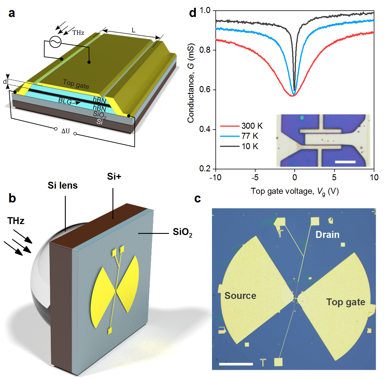
There are three crucial steps to consider in the design of resonant photodetectors. First, the incoming radiation needs to be efficiently compressed into plasmons propagating in the FET channel. Second, the channel should act as a high-quality plasmonic cavity, where constructive interference of propagating plasma waves leads to the enhancement of the field strength. Third, the high-frequency plasmon field needs to be rectified into a dc photovoltage. To meet these hard-to-satisfy Vicarelli2012 ; Spirito2014 ; Tong2015 ; Qin2017 requirements, we fabricated proof-of-concept detectors using high-mobility bilayer graphene (BLG) FETs. To this end, we first applied a standard dry transfer technique to encapsulate BLG between two relatively thin ( nm) slabs of hBN Kretinin2014 . The heterostructure had side contacts (Fig. 1a) which were extended to the millimeter scale and one of them served as a sleeve of the broadband antenna, Fig. 1c and Supplementary Fig. 3a-b (see Methods). Another antenna sleeve was connected to the top gate covering the FET channel (inset of Fig. 1d). In this coupling geometry, the incident radiation induces high-frequency modulation of the gate-to-channel voltage thereby launching plasma waves from the source terminal Dyakonov1996a . The detector was assembled on a THz–transparent Si wafer attached to a Si lens focusing the incident radiation onto the antenna (Fig. 1b).
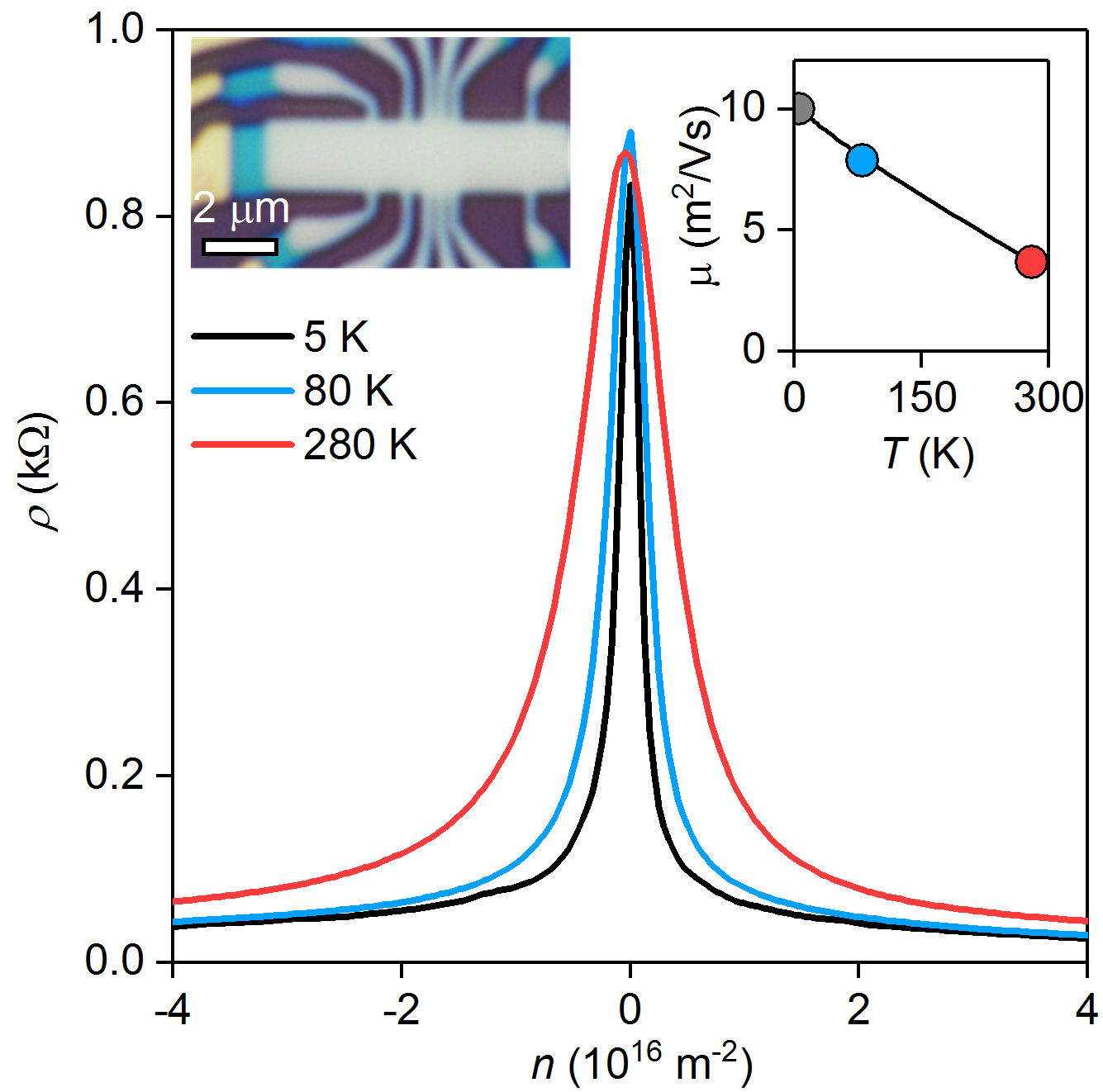
We studied four BLG FETs, from to m in length and from to m in width , all exhibiting typical field-effect behaviour as seen from measurements of the conductance (Fig. 1d and Supplementary Fig. 3e). In particular, is minimal at the charge neutrality point and rises with increasing . The mobility of our devices at the characteristic carrier density cm-2 exceeded and remained above at temperatures K and K, respectively, as determined from the characterization of a multiterminal Hall bar produced under identical protocol reported in Methods (Supplementary Note 1 and Supplementary Fig. 1).
Broadband operation
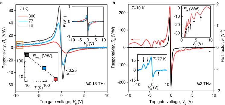
We intentionally start the photoresponse measurements at the low end of the sub-THz domain, where the plasma oscillations are overdamped (see below). This allows us to compare the performance of our detectors with previous reports Vicarelli2012 ; Spirito2014 ; LKoppens2014 ; Tong2015 ; Qin2017 . Figure 2a shows an example of the responsivity , where is the emerging source-to-drain photovoltage and is the incident radiation power, as a function of the top gate voltage under irradiation with frequency THz in one of our BLG detectors (see Methods). In good agreement with the previous studies, the dependence follows the evolution of the FET-factor , shown in the inset of Fig. 2a. In particular, increases in magnitude upon approaching the charge neutrality point (NP) where it flips sign because of the change in charge carrier type.
We have studied the operation of our detectors at different temperatures and found that grows with decreasing (bottom inset of Fig. 2a) and reaches its maximum V/W at K due to a steeper at this (top inset of Fig. 2a). At large positive , approaches zero at all , whereas at negative , a positive offset is observed (orange rectangle in Fig. 2a). This behaviour is common for this type of devices and is related to additional rectification by p-n junctions at the boundaries between the p-doped graphene channel and the n-doped contact regions Cai2014 ; Ryzhii2006 ; Bandurin2017 .
The overall broadband responsivity of our BLG detectors is further improved in transistors with stronger nonlinearity, which can be conveniently parametrized by the FET-factor introduced above. To this end, we took advantage of the gate-tunable band structure of BLG and fabricated a dual-gated photodetector. Simultaneous action of the two gates results in a band gap opening and a steep dependence that, in turn, causes a drastic enhancement of (Supplementary Note 2). The latter exceeded 3 kV/W for a weak displacement field of 0.1 V/nm (Supplementary Fig. 2b). This translates to the noise equivalent power (NEP) of about pW/Hz1/2, estimated using the Johnson-Nyquist noise spectral density obtained for the same . The observed performance of our detectors makes them competitive not only with other graphene-based THz detectors operating in the broadband regime LKoppens2014 , but also with some commercial superconducting and semiconductor bolometers operating at the same and (Supplementary Table 1).
Resonant photoresponse
The response of our photodetectors changes drastically as the frequency of incident radiation is increased. Fig. 2b shows the gate voltage dependence of recorded in response to THz radiation. In stark contrast to Fig. 2a, exhibits prominent oscillations, despite the fact that as a function of is featureless (black curve in Fig. 2b). The oscillations are clearly visible for both electron and hole doping and display better contrast on the hole side, likely because of the aforementioned p-n junction rectification. Resonances are well discerned at , although they persist up to liquid-nitrogen , especially for . A further example of resonant operation of another BLG device is shown in Supplementary Note 3.
We have also studied the performance of our detectors at intermediate frequencies and found that the resonant operation of our devices onsets in the middle of the sub-THz domain (Supplementary Note 4). In particular, we have found that at GHz, the resonances are already well-developed (Supplementary Fig. 4). At such low , only two peaks in the photoresponse (one for electrons and one for holes) are observed for the same gate voltage span as in Fig. 2b along with an apparent increase of their full width at half-height. These observations are in full agreement with the plasmon-assisted photodetection model discussed below.
Plasmon resonances in graphene FETs
We argue that the observed peaks in the photoresponse emerge as a result of plasmon resonance in the FET channel. To this end, we model our FET as a plasmonic Fabry-Perot cavity endowed with a rectifying element. This results in responsivity given by
| (1) |
where is a smooth function of carrier density and frequency that depends on the microscopic rectification mechanism, and are the wave reflection coefficients from the source and drain terminals, respectively, and is the complex wave vector governing the wave propagation in the channel (Supplementary Note 5). In gated 2D electron systems, the relation between the frequency and the real part of the wave vector is linear, , where the plasmon phase velocity is
| (2) |
Here and are the effective mass of carriers and the elementary charge respectively, and are the Fermi velocity and the Fermi wave vector, is the distance to the gate, is the dimensionless coupling constant and is the out-of-plane dielectric permittivityChaplik1972 ; Tomadin2013 . We further note that eq. (2) is valid for monolayer graphene upon replacement of the effective mass with the cyclotron mass, (see Supporting Note 6). The latter increases with gate-induced carrier density , thereby limiting the tuning range of for a given voltage span. In contrast, in the case of BLG, is nearly constant () for experimentally accessible values of , a feature that allows us to vary over a wider range and thus switch the detector between multiple modes, as we now proceed to show.
It follows from eq. (1), that the responsivity of our Fabry-Perot rectifier is expected to peak whenever the denominator in eq. (1) approaches zero. In our devices, the source potential is clamped to antenna voltage, and no ac current flows into the drain, therefore (Ref. (3; 32)). The resonances should therefore occur whenever the real part of the wave number is quantized according to
| (3) |
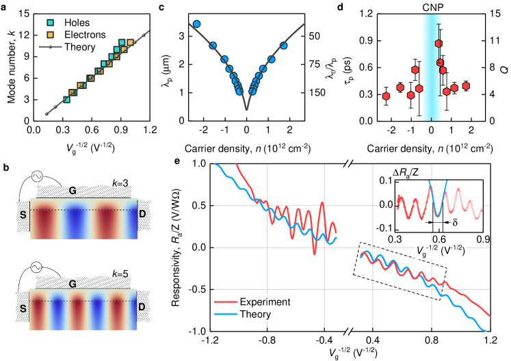
The quantization rule (3) combined with eq. (2) predicts a linear dependence of the mode number on which may serve as a benchmark for plasmon resonances in the FET channel. This is indeed the case of our photodetector, as shown in Figs. 3a,e and Supplementary Fig. 3c. The slope of the experimental dependence in Fig. 3a matches well the theoretical expectation for a BLG Fabry-Perot cavity of length m. At large , we find a slight upward trend in the experimental data with respect to the linear dependence. We attribute this trend to deviations of the plasmon dispersion from the linear law at short wavelengths which stem from the non-local relation between electric potential and carrier density Chaplik1972 . Note that the known non-parabolicity of the BLG spectrum Zou2011 resulting in an increase of at large density would bend the dependence in Fig. 3a in the opposite direction.
Photovoltage-based spectroscopy of 2D plasmons
The resonant gate-tunable response of our detectors offers a convenient tool to characterize plasmon modes in graphene channels. From eq. (3) it follows that resonances occur if , where is the plasmon wavelength (Fig. 3b). Using the experimentally observed peak positions, we have determined the density dependence of , shown in Fig. 3c, which flaunts excellent agreement with theory. The compression ratio between the plasmon and free-space wavelength ( and the speed of light in vacuum) ranges between and , highlighting the ultra-strong confinement of THz fields enabled by graphene plasmons, matching the record value known in the literature Woessner2015 .
Apart from , the resonant responsivity carries information about another valuable characteristic of plasmons, namely, their lifetime, . The latter is related to the peak width at half-height via (Supplementary Note 7)
| (4) |
Using Lorentzian fits to the photoresponse curves (inset of Fig. 3e), we have extracted as a function of , shown in Fig. 3d. The lifetime was found to range between and , which is slightly shorter than the transport time as extracted from the mobility, (Supplementary Note 1). The corresponding quality factor, , was found to vary between and for , and between and for , see Fig. 3d. The latter implies that it is unreasonable to expect resonant photoresponse of such detectors in the GHz range, and they can only operate in the broadband (non-resonant) regime, in accordance with the data in Fig. 2a. On the contrary, the resonant responsivity should become more profound at higher frequencies of the THz window and can be further enhanced in graphene FETs of higher quality, such as those using graphite gates to screen remote charge impurities AFY2018 .
Miniband plasmons in graphene/hBN superlattices
The approach demonstrated above is universal and can be applied to studies of plasmons in arbitrary high-mobility 2D systems embedded in FET channels, as we now proceed to show for the case of devices made of BLG/hBN moiré superlattices Mucha-Kruczyński2013 .
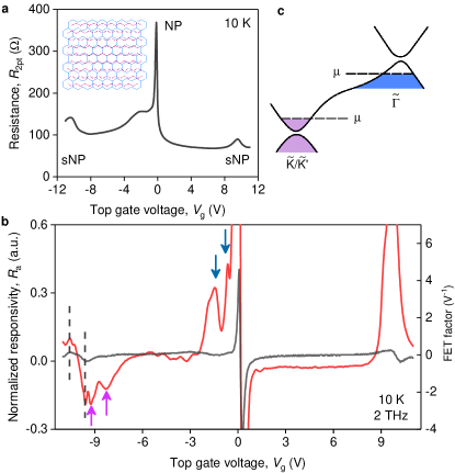
Figures 4b and Supplementary Fig. 3c show examples of as a function of recorded in our superlattice devices in response to 2 THz radiation. As in the case of plain BLG, the overall evolution of the superlattice responsivity follows that of the FET-factor (black curve) modulated by the plasmon resonances. Note the total number of resonances is smaller due to the shorter FET channel (cf. Supplementary Fig. 3c) and they are visible only for , presumably due to a stronger nonlinearity in this detector for negative doping (in another superlattice FET, the resonances were well-observed for both polarities as shown in Supplementary Fig. 3c). Importantly, the FET-factor in these devices is, in turn, a more complex function of (cf. inset of Fig. 2a) due the presence of secondary neutrality points (sNP) stemming from a peculiar band structure of the BLG/hBN superlattice. The latter is characterized by narrow minibands emerging in the vicinity of the -points of the superlattice Brillouin zone Mucha-Kruczyński2013 (Fig. 4c). The sNPs are clearly visible as peaks in the FET resistance which appear around V (Fig. 4a).
A striking feature of the superlattice photoresponse is the resonances appearing when the Fermi level is brought close to the sNP (pink arrows in Fig. 4b). The resonances are of opposite sign with respect to those observed near the main NP (blue arrows), which indicates that they originate from the plasmons supported by the charge carriers of the opposite type (cf. Fig. 2b). Since the latter are hosted by the minibands near the -points of the superlattice Brillouin zone (Fig. 4c), our measurements provide evidence for miniband plasmons that were long identified theoretically Tomadin2014 but remained elusive in experiment. To date, the experimental studies of superlattice plasmons have been only performed at room temperature using scattering-type scanning near field microscopy operating in the mid-IR domain Ni2015 . The mid-IR excitation energy (10 m meV) is high enough to induce interband absorption close to the sNP, which hampers the observation of plasmons in superlattice minibands (39). In contrast, our approach relies on the low-energy excitations (2 THz meV), is applicable at cryogenic temperatures, and, therefore, paves a convenient way for further studies of miniband plasmonics.
DISCUSSION
Resonant responsivity is a universal phenomenon in ultra-clean graphene devices and is expected to be independent of the physical mechanisms behind the rectification of the ac field into a dc photovoltage. Nevertheless, it is important to establish possible nonlinearities responsible for the rectification, for example, in order to be able to increase the magnitude of responsivity.
We first note that the aforementioned asymmetry in between electron and hole doping indicates rectification at the - junction formed in vicinity of the contacts. This rectification usually appears due to the thermoelectric effect arising as a result of non-uniform sample heating and the difference between the Seebeck coefficients in the graphene channel and contact regionsCai2014 ; Alonso-Gonzalez2016 ; Jung2016 ; Bandurin2017 (Supplementary Note 8). However, remains finite even for , where both channel and contact areas are -doped. This indicates that alternative rectification mechanisms are also involved.
Another commonly accepted mechanism is the rectification arising as a result of the simultaneous action of longitudinal high-frequency field and modulation of channel conductivity, also known as resistive self-mixing Daryoosh2013 . The latter can be enhanced by the dc photovoltage that balances the difference between electron kinetic energies at the source and drain terminals Dyakonov1996a ; Daryoosh2013 , similar to Bernoulli’s law for classical fluids. Both mechanisms are combined into so-called Dyakonov- Shur (DS) rectification Dyakonov1996a and result in proportional to the sensitivity of the conductivity to the gate voltage variation Knap2009 , given by the -factor introduced above (Supplementary Note 9). In Fig. 3e we compare the resonant photoresponse of our BLG photodetector with the responsivity expected from the DS model Dyakonov1996a assuming an average ps, as found from Fig. 3d, and using the effective antenna impedance as the only fitting parameter. The two curves show the same functional behaviour and match quantitatively for the n-doped case (where the p-n junction is absent) and , a value close to that expected from the equivalent circuit design Bandurin2017 . We further note, that although the original DS proposal was based on the hydrodynamic electron transport BandurinFO201 ; Berdyugin2018 , an identical photoresponse is expected outside the hydrodynamic window as it follows from the analysis of graphene’s nonlinear conductivity Alepr2018 .
Last but not least, we note that while the overall trend of the responsivity is well-described by the model introduced above, the values of extracted from the peak width at half-height are found to be below the momentum relaxation time. This suggests that other mechanisms of resonance broadening are also involved. In particular, leakage of plasma waves into metal contacts Satou2009 and electromagnetic dissipation in antenna may also contribute to the apparent resonance width. We have found that respective contributions to are most pronounced at large carrier densities and small harmonic numbers (Supplementary Figs. 6 and 7), in agreement with experimental data in Fig. 3d. Elimination of these damping channels, e.g. with Schottky/tunnel contacts and low-impedance antennas, may extend the resonant detection down to tens of gigahertz Graef2018 . Other dissipation channels such as electron viscosity Kumar2017 ; Svintsov2017 and interband absorption Chen2012 should be most pronounced at higher-order harmonics and in the vicinity of the NP, as opposed to the data in Fig. 3d, and are unlikely relevant to the present study.
In conclusion, we have shown that high-mobility graphene FETs exploiting far-field coupling to incoming radiation can operate as resonant THz photodetectors. In addition to their potential applications in high-responsivity detection and on-chip spectroscopy of the THz radiation, our devices also represent a convenient tool to study plasmons under conditions where other approaches may be technically challenging. Due to their compact size and far-field coupling, our photodetectors can easily be employed to carry out plasmonic experiments in extreme cryogenic environments and in strong magnetic fields, as well in studies of more complex van der Waals heterostructures. As an example, we have demonstrated the use of our approach to reveal low-energy plasmons hosted by moiré minibands in BLG/hBN superlattices. The method has a strong potential for studies of collective modes in magnetic minibands which have recently gained a great level of attention KrishnaKumar2017 .
METHODS
Device fabrication
All our devices were made of BLG. BLG was first encapsulated between relatively thick hBN crystals using the standard dry-peel technique Kretinin2014 . The thickness of the top hBN was measured by atomic force microscopy. The stack was then deposited either directly on top of a low-conductivity boron-doped silicon wafer capped with a thin oxide layer ( nm) or on a predefined back gate electrode. The resulting van der Waals heterostructure was patterned using electron beam lithography to define contact regions. Reactive ion etching was then used to selectively remove the areas unprotected by a lithographic mask, resulting in trenches for depositing electrical leads. Metal contacts to graphene were made by evaporating 3 nm of Cr and 60 nm of Au. Afterwards, a second e-beam lithography was used to design the top gate. The graphene channel was finally defined by a third round of e-beam lithography, followed by reactive ion etching etching using Poly(methyl methacrylate) and gold top gate as the etching mask. Finally, we used optical photolithography to pattern large antenna (spiral or bow-tie) sleeves connected to the source and the top-gate terminals, followed by evaporation of 3 nm of Cr and 400 nm of Au. Antennas were designed to operate at an experimentally accessible frequency range.
Photoresponse measurements
Photoresponse measurements were performed in a variable temperature optical cryostat equipped with a polyethylene window that allowed us to couple the photodetector to incident THz radiation. The latter was focused to the device antenna by a silicon hemispherical lens attached the silicon side of the chip (Fig. 1b). The transparency of the chips to THz radiation over the entire temperature and frequency range was verified in transmission experiments using a home-made optical cryostat coupled to the THz spectrometer. Photovoltage measurements were performed using either a standard lockin amplifier synchronized with a chopper rotating at 1 kHz frequency, positioned between the radiation source and the cryostat window, or by a home-made measurement board.
In order to study the photoresponse of our detectors at different frequencies, we used three radiation sources. Sub-THz radiation was provided by two backward wave oscillators (BWO) generating THz and THz. For higher frequencies, a quantum cascade continues wave laser based on a GaAs/Al0.1Ga0.9As heterostructure emitting THz radiation was used.
The responsivity of our devices was calculated assuming that the full power delivered to the device antenna funnelled into the FET channel. The as-determined value provides the lower bound for our detectors’ responsivity and is usually referred to as extrinsic. The calculation procedure consisted of a few steps. First the source-to-drain voltage was measured as a function of in the dark. Then, the dependence of the source-to-drain voltage on was recorded under illumination with THz radiation. The difference formed the photovoltage. At the next stage, we measured the full power delivered to the cryostat window using Golay cell. The responsivity was then calculated as , where is the power delivered to the device antenna after accounting for losses in the silicon lens and the cryostat optical window ( dB). All the measurements reported above were performed in the linear-in- regime. The performance of our detectors outside the linear regime is discussed in Supplementary Note 10 and reported in Supplementary Fig. 8.
Data availability
The data that support the findings of this study are available from the corresponding author upon reasonable request.
Acknowledgements
Device fabrication and Manchester’s part of the work was supported by the European Research Council, the Graphene Flagship and Lloyd’s Register Foundation. The work at the MSPU (Photoresponse measurements) has been carried out with the support of the Russian Science Foundation (project No. 17-72-30036). D.A.B. acknowledges financial support from Leverhulme Trust. Experimental work of M.M. (transport measurements) was supported by Russian Science Foundation (Grant 18-72-00234). M.P. is supported by the European Union’s Horizon 2020 research and innovation programme under grant agreement No. 785219 - GrapheneCore2. Modelling of antenna electrodynamics was supported by RFBR (Project 18-29-20116). Theoretical work of D.S. was supported by the grant 16-19-10557 of the Russian Science Foundation. Photoresponse measurements have been performed using quantum cascade laser fabricated by A. Valavanis in the group of Prof. Dragan Indjin in the University of Leeds (UK). We thank A. Tomadin, R. Krishna Kumar, A. Berdyugin, L. Levitov and V. Fal’ko for fruitful discussions.
Author contributions
D.A.B. and G.F. designed and supervised the project. S.G.X. and I.G. fabricated the devices. Photoresponse measurements were carried out by I.G., M.M and D.A.B. Data analysis was performed by D.A.B. and D.S. Theory analysis was done by D.S. The manuscript was written by D.A.B. and D.S. with input from I.V.G., M.P., A.P. and A.K.G. Experimental support was provided by I.T., D. Y., S.Z. and G.G. T.T. and K.W. grew the hBN crystals. All authors contributed to discussions.
Competing interests
The authors declare no competing interests.
References
- (1) Dhillon, S. S. et al. The 2017 terahertz science and technology roadmap. Journal of Physics D: Applied Physics 50, 043001 (2017).
- (2) Daryoosh, S. Handbook of terahertz technology for imaging, sensing and communications Woodhead Publishing (2013).
- (3) Dyakonov, M. & Shur, M. Detection, mixing, and frequency multiplication of terahertz radiation by two-dimensional electronic fluid. IEEE Transactions on Electron Devices 43, 380–387 (1996).
- (4) Knap, W. et al. Field effect transistors for terahertz detection: Physics and first imaging applications. Journal of Infrared, Millimeter, and Terahertz Waves 30, 1319–1337 (2009).
- (5) Vicarelli, L. et al. Graphene field-effect transistors as room-temperature terahertz detectors. Nature Materials 11, 865–871 (2012).
- (6) Spirito, D. et al. High performance bilayer-graphene Terahertz detectors. Applied Physics Letters 104, 061111 (2014).
- (7) Tong, J., Muthee, M., Chen, S. Y., Yngvesson, S. K. & Yan, J. Antenna Enhanced Graphene THz Emitter and Detector. Nano Letters 15, 5295–5301 (2015).
- (8) Qin, H. et al. Room-temperature, low-impedance and high-sensitivity terahertz direct detector based on bilayer graphene field-effect transistor. Carbon 116, 760–765 (2017).
- (9) Generalov, A. A., Andersson, M. A., Yang, X., Vorobiev, A. & Stake, J. A 400-GHz Graphene FET Detector. IEEE Transactions on Terahertz Science and Technology 7, 614–616 (2017).
- (10) Peralta, X. G. et al. Terahertz photoconductivity and plasmon modes in double-quantum-well field-effect transistors. Appl. Phys. Lett. 81, 1627–1629 (2002).
- (11) Knap, W., Deng, Y., Rumyantsev, S. & Shur, M. S. Resonant detection of subterahertz and terahertz radiation by plasma waves in submicron field-effect transistors. Appl. Phys. Lett. 81, 4637–4639 (2002).
- (12) Teppe, F. et al. Room-temperature plasma waves resonant detection of sub-terahertz radiation by nanometer field-effect transistor. Applied Physics Letters 87, 85–88 (2005).
- (13) Muravev, V. M. & Kukushkin, I. V. Plasmonic detector/spectrometer of subterahertz radiation based on two-dimensional electron system with embedded defect. Appl. Phys. Lett. 100, 082102 (2012).
- (14) Giliberti, V. et al. Downconversion of terahertz radiation due to intrinsic hydrodynamic nonlinearity of a two-dimensional electron plasma. Physical Review B 91, 165313 (2015).
- (15) Ju, L. et al. Graphene plasmonics for tunable terahertz metamaterials. Nature Nanotechnology 6, 630–634 (2011).
- (16) Yan, H. et al. Tunable infrared plasmonic devices using graphene/insulator stacks. Nature Nanotechnology 7, 330–334 (2012).
- (17) Fei, Z. et al. Gate-tuning of graphene plasmons revealed by infrared nano-imaging. Nature 486, 82–85 (2012).
- (18) Chen, J. et al. Optical nano-imaging of gate-tunable graphene plasmons. Nature 487, 77–81 (2012).
- (19) Grigorenko, A., Polini, M. & Novoselov, K. Graphene plasmonics. Nature Photonics 6, 749 – 758 (2012).
- (20) Woessner, A. et al. Highly confined low-loss plasmons in graphene-boron nitride heterostructures. Nature Materials 14, 421–425 (2015).
- (21) Alonso-González, P. et al. Acoustic terahertz graphene plasmons revealed by photocurrent nanoscopy. Nature Nanotechnology 12, 31–36 (2016).
- (22) Ni, G. et al. Fundamental limits to graphene plasmonics. Nature 557, 530–533 (2018).
- (23) Koppens, F. H. L. et al. Photodetectors based on graphene, other two-dimensional materials and hybrid systems. Nature Nanotechnology 9, 780–793 (2014).
- (24) Cai, X. et al. Sensitive room-temperature terahertz detection via the photothermoelectric effect in graphene. Nature Nanotechnology 9, 814–819 (2014).
- (25) Auton, G. et al. Terahertz Detection and Imaging Using Graphene Ballistic Rectifiers. Nano Letters 17, 7015–7020 (2017).
- (26) Otsuji, T., Hanabe, M., Nishimura, T. & Sano, E. A grating-bicoupled plasma-wave photomixer with resonant-cavity enhanced structure. Optics express 14, 4815–4825 (2006).
- (27) Tomadin, A., Tredicucci, A., Pellegrini, V., Vitiello, M. S. & Polini, M. Photocurrent-based detection of terahertz radiation in graphene. Applied Physics Letters 103, 211120 (2013).
- (28) Ryzhii, V., Otsuji, T., Ryzhii, M. & Shur, M. S. Double graphene-layer plasma resonances terahertz detector. J. Phys. D: Appl. Phys. 45, 302001 (2012).
- (29) Fateev, D. V., Mashinsky, K. V. & Popov, V. V. Terahertz plasmonic rectification in a spatially periodic graphene. Appl. Phys. Lett. 110, 061106 (2017).
- (30) Kretinin, A. V. et al. Electronic properties of graphene encapsulated with different two-dimensional atomic crystals. Nano Letters 14, 3270–3276 (2014).
- (31) Ryzhii, V. & Shur, M. S. Resonant terahertz detector utilizing plasma oscillations in two-dimensional electron system with lateral schottky junction. Jpn. J. Appl. Phys. 45, L1118 (2006).
- (32) Bandurin, D. A. et al. Dual origin of room temperature sub-terahertz photoresponse in graphene field effect transistors. Applied Physics Letters 112, 141101 (2018).
- (33) Chaplik, A. Possible crystallization of charge carriers in low-density inversion layers. Sov. Phys. JETP 35, 395 (1972).
- (34) Tomadin, A. & Polini, M. Theory of the plasma-wave photoresponse of a gated graphene sheet. Phys. Rev. B 88, 205426 (2013).
- (35) Zou, K., Hong, X. & Zhu, J. Effective mass of electrons and holes in bilayer graphene: Electron-hole asymmetry and electron-electron interaction. Phys. Rev. B 84, 085408 (2011).
- (36) Zibrov, A. A. et al. Tunable interacting composite fermion phases in a half-filled bilayer-graphene Landau level. Nature 549, 360–364 (2017).
- (37) Mucha-Kruczyński, M., Wallbank, J. & Fal’Ko, V. Heterostructures of bilayer graphene and h-BN: Interplay between misalignment, interlayer asymmetry, and trigonal warping. Phys. Rev. B 90, 205418 (2013).
- (38) Tomadin, A., Guinea, F. & Polini, M. Generation and morphing of plasmons in graphene superlattices. Phys. Rev. B 90, 161406(R) (2014).
- (39) Ni, G. et al. Plasmons in graphene moiré superlattices. Nature Materials 14, 1217–1222 (2015).
- (40) Jung, M., Rickhaus, P., Zihlmann, S., Makk, P. & Schonenberger, C. Microwave Photodetection in an Ultraclean Suspended Bilayer Graphene p-n Junction. Nano Letters 16, 6988–6993 (2016).
- (41) Bandurin, D. et al. Fluidity onset in graphene. Nature Communications 4533 (2018).
- (42) Berdyugin, A. et al. Measuring Hall Viscosity of Graphene’s Electron Fluid. arXiv:1806.01606 (2018).
- (43) Principi, A., Bandurin, D., Rostami, H. & Polini, M. Pseudo-Euler equations from nonlinear optics: plasmon-assisted photodetection beyond hydrodynamics. arXiv:1811.06540 (2018).
- (44) Satou, A., Ryzhii, V., Mitin, V. & Vagidov, N. Damping of plasma waves in two-dimensional electron systems due to contacts. Physica Status Solidi (B) 246, 2146–2149 (2009).
- (45) Graef, H. et al. Ultra-long wavelength Dirac plasmons in graphene capacitors. J. Phys. Mater. 01LT02 (2018).
- (46) Kumar, R. K. et al. Superballistic flow of viscous electron fluid through graphene constrictions. Nature Physics 13, 1182–1185 (2017).
- (47) Svintsov, D. Hydrodynamic-to-ballistic crossover in dirac materials. Phys. Rev. B 97, 121405 (2018).
- (48) Krishna Kumar, R. et al. High-temperature quantum oscillations caused by recurring Bloch states in graphene superlattices. Science 357, 181–184 (2017).
- (49) Aizin, G. R. & Dyer, G. C. Transmission line theory of collective plasma excitations in periodic two-dimensional electron systems: Finite plasmonic crystals and tamm states. Phys. Rev. B 86, 235316 (2012).
- (50) Dyer, G. C. et al. Induced transparency by coupling of tamm and defect states in tunable terahertz plasmonic crystals. Nature Photonics 7, 925 (2013).
- (51) Collin, R. E. Field theory of guided waves (McGraw-Hill, 1960).
- (52) Das Sarma, S., Adam, S., Hwang, E. H. & Rossi, E. Electronic transport in two-dimensional graphene. Rev. Mod. Phys. 83, 407–470 (2011).
- (53) Low, T., Perebeinos, V., Kim, R., Freitag, M. & Avouris, P. Cooling of photoexcited carriers in graphene by internal and substrate phonons. Phys. Rev. B 86, 045413 (2012).
Supplementary Note 1: Device characterization
Our photodetectors represent two-terminal field-effect transistors (FET) and, therefore, the measured conductance (Fig. 1d of the main text), which contains non-zero contribution from the BLG-metal contact, does not provide the information on the quality of the FET channel. In order to estimate the mobility of charge carriers in the BLG channel, we fabricated a reference multi-terminal Hall bar using the same procedure as described in Methods. The Hall bar was characterized using the standard four-terminal geometry that involved the measurements of its sheet resistance as a function of carrier density and temperature (Supplementary Fig. 1). One can see a typical field-effect behavior for high-quality graphene that manifests itself in sharp peak in at the charge neutrality point which decays steeply with increasing . The charge carrier mobility was calculated using the Drude formula, , and for typical cm-2 exceeded 10 m2/Vs at liquid helium and remained around 2.5 m2/Vs at room temperature.
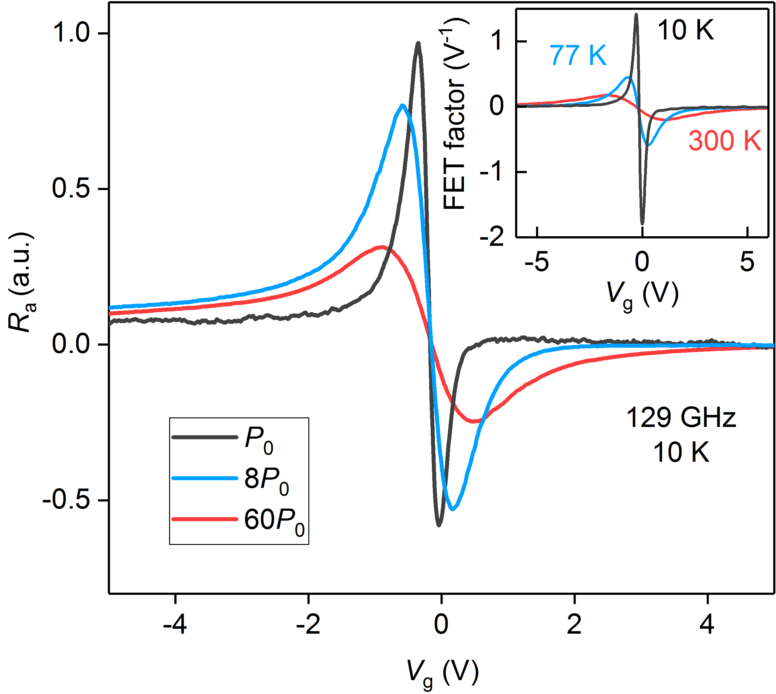
Supplementary Note 2: High-responsivity THz detection in dual-gated BLG field effect transistors
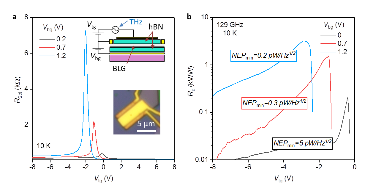
As discussed in the main text, the responsivity of the THz detectors made of the field effect transistors is proportional to the sensitivity of the FET conductivity to the gate voltage variation. To improve the performance of our detectors, we took advantage of BLG’s gate-tunable band structure and fabricated a dual-gated device (top and bottom insets of Supplementary Fig. 2a). The idea is that when an electric field is applied perpendicular to the channel it induces a band gap in BLG that leads to a steeper dependence of the FET resistance on the gate voltage. Supplementary Fig. 2a shows examples of dependences measured at few demonstrating the expected increase of with increasing the average displacement field applied to BLG, where () is the thickness of the bottom (top) hBN crystal and is its dielectric constant.
Supplementary Fig. 2b shows the top gate voltage dependence of measured in response to 0.13 THz radiation in the dual-gated detector. In the case of zero back gate voltage (black curve), repeats the behaviour of another detector reported in Fig. 2a of the main text. Namely, the responsivity reaches its maximum of about 200 V/W near the NP where it flips its sign because of the change in the charge carrier type. Note, the absolute value of the maximum responsivity is very close to that reported in the main text (Fig. 2b) highlighting the reproducibility of our detectors’ performance. When the back gate voltage is applied, the responsivity increases drastically (red and blue curves in Supplementary Fig. 2b). Already for a moderate V/nm the responsivity increases by more than an order of magnitude and exceeds 3 kV/W. The corresponding noise equivalent power, estimated using the Johnson-Nyquist noise spectral density for the same , reaches 0.2 pW/Hz1/2. This makes our detector competitive not only with other graphene-based THz detectors LKoppens2014 but also with some commercial semiconductor and superconductor bolometers (Table 1).
| Detector | NEP, pW/Hz0.5 | Operation Temperature, K | Reference | |||||
|
0.1 - 1 | 2.5 - 4.5 |
|
|||||
|
0.04 - 0.8 | 1.6 - 4.2 | www.infraredlaboratories.com | |||||
|
0.2 | 10 | This work |
Supplementary Note 3: Further examples of resonant photoresponse
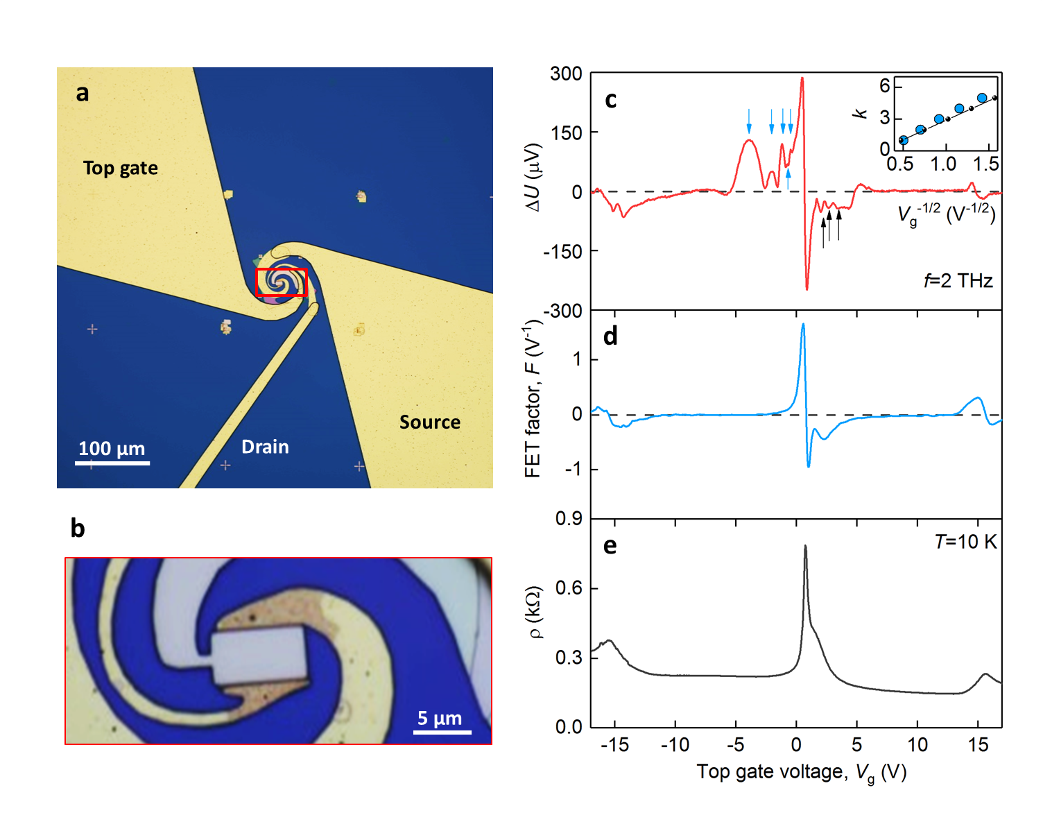
To illustrate that the observed resonant photoresponse is reproducible for different electronic systems embedded in FETs of various lengths and coupled to different antennas, Supplementary Fig. 3c shows another example of the photovoltage emerging when the incoming 2 THz radiation is coupled to the broadband logarithmic spiral antenna connected to another FET. The latter is made of BLG having its crystallographic axis aligned with those of hBN, that reveals itself in peculiar three-peaks structure, shown in Supplementary Fig. 3e. The photoresponse curves are rather similar to those shown in Supplementary Fig. 2b of the main text, namely they follow the envelope trend set by the FET-factor (Supplementary Fig. 3d) superimposed with the resonant peaks. The resonances are periodic in (inset to Supplementary Fig. 3c) and are clearly seen for both electron and hole doping. Importantly, on the contrary to Fig. 2b, the photoresponse now changes sign multiple times following non-trivial evolution.
Supplementary Note 4: Resonant detection of sub-THz radiation
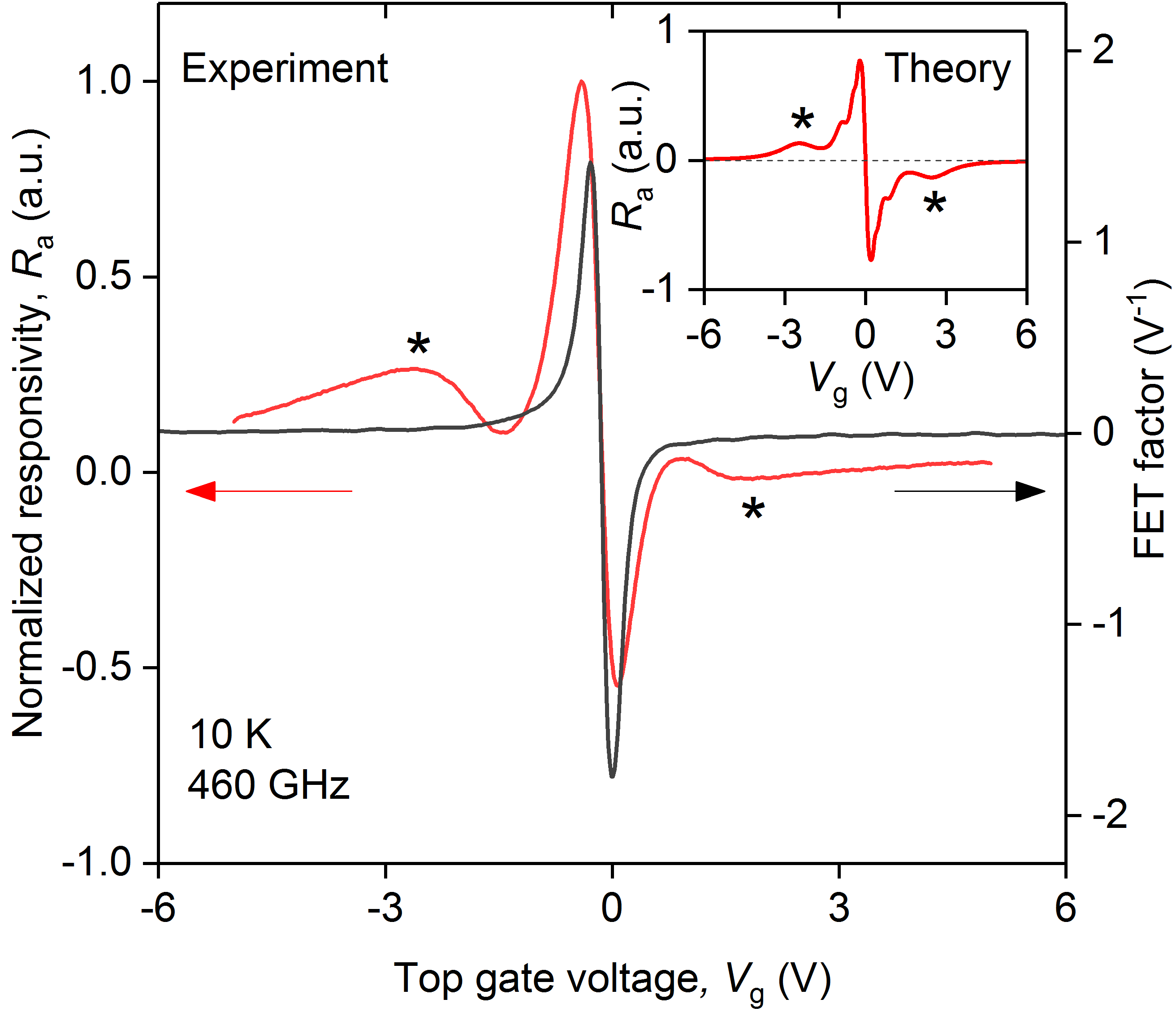
We have also studied the performance of our detectors at frequencies intermediate to those reported in Figs. 2a and b of the main text and found that the resonant operation onsets already in the middle of the sub-THz domain. Figure 4 shows the gate voltage dependence of recorded in response to 460 GHz radiation. In the vicinity of the charge neutrality point (NP) the responsivity peaks and changes its sign in agreement with the evolution of the FET-factor with the gate voltage (black curve in Supplementary Fig. 4) as discussed in the main text. However, away from the NP the responsivity peaks for both electron and hole doping (stars in Supplementary Fig. 4) despite the fact that is featureless. These peaks stem from the plasmon resonances in the FET channel as it follows from the comparison of the experimental data with theory (inset of Supplementary Fig. 4). In good agreement with theory, at lower frequencies the number of resonant modes, which can be observed for the same gate voltage span, is smaller compared to that found at 2 THz (Fig. 2b of the main text). In addition, the resonances appear much broader than those observed at 2 THz (Fig. 2b) which is consistent with the reduced quality factor at sub-THz frequencies.
Supplementary Note 5: Fabri-Perot cavity model for plasmonic field-effect transistor
Gated two-dimensional electronic systems support plasma waves with the dispersion relation Chaplik1972
| (1) |
where and are the plasmon wavelength and wave vector, respectively, is the momentum relaxation time, is the carrier density, is the effective mass of charge carriers, it the distance to the gate, is the dielectric permittivity, and is the vacuum permittivity.
Confinement of a 2d channel by source and drain contacts quantizes the wave vector and leads to emergence of discrete plasmon frequencies. The quantization conditions can be obtained by requiring the oscillating quantity (e.g. voltage ) to return to its original value after the channel round trip:
| (2) |
where and are the complex-valued reflection coefficients at the source and drain terminals, respectively. Therefore, eigen frequencies of bounded plasmons can be found from
| (3) |
To see that the latter dispersion relation indeed appears in the nonlinear response functions, we model the FET channel as a transmission line (TL) fed by antenna voltage at the source side Aizin2012 ; dyer2013 . The antenna may have finite impedance which will be taken into account at the end of this section. The TL is terminated by load impedance at the drain side, and by impedance at the source side. In real device, these impedances are due to the capacitive coupling between the respective electrodes. The TL model is justified by the formal coincidence of TL equations (Telegrapher’s equation) with transport equations in a gated FET channel.
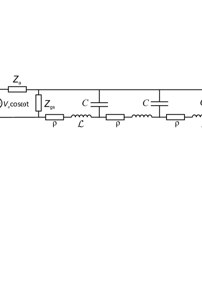
The TL elements are specific inductance
| (4) |
capacitance per unit length
| (5) |
and resistance
| (6) |
where is the channel width. It is readily seen that the dispersion relation for waves in an infinite transmission line collin1960
| (7) |
coincides with plasma wave dispersion (1) with proper values of line parameters (4-6). The characteristic (wave) impedance of transmission line is
| (8) |
A well-known result for current reflection coefficient from a loaded (drain) end of transmission line reads
| (9) |
while for source end with fixed voltage
| (10) |
When the reflection coefficients and conditions at the ends of cavity are specified, it is straightforward to write down the solution for voltage across the TL (which is the gate-to-channel voltage in the actual FET):
| (11) |
here and are given by Eqs. (9) and (10), respectively. The longitudinal electric field in the channel is given by
| (12) |
As the nonlinear response of the FET is proportional to the properly averaged square of ac electric field in the channel (12), it becomes apparent that responsivity would possess a plasma resonant factor , independent of the detection mechanism.
The account of finite antenna impedance results in a a simple ”renormalization” of input voltage in Eqs. (11) and (12):
| (13) |
where stands for parallel connection of impedances, and is the input impedance of the transmission line (we have used ). It is straightforward to show that the modification of input voltage can be translated in the modification of ”resonant denominator”
| (14) |
The effect of in the square bracket is the reduction of input voltage due to the drop at internal antenna resistance. Finite value of in the second term leads to extra broadening or resonances, as analyzed below.
Supplementary Note 6: Gate tuning of graphene plasmons: monolayer vs bilayer
We briefly review the density dependences of plasmon frequencies in single layer graphene (SLG) and bilayer graphene (BLG). The general dispersion relation for gated plasmons in two-dimensional electron system with sheet conductivity reads Chaplik1972
| (15) |
The study of plasmon dispersions in various two-dimensional systems is therefore reduced to evaluation of their frequency-dependent conductivity. In the classical () long-wavelength () limit, the latter is found from the Boltzmann equation DasSarma2011
| (16) |
where is the density of states, is the velocity of carrier with momentum , and is the equilibrium distribution function. In case of BLG, , , which results in ordinary Drude conductivity
| (17) |
In case of SLG, , , and the conductivity reads
| (18) |
The latter equality is valid at low temperatures. Using the low-temperature relation between density and Fermi energy in SLG , we readily observe that classical conductivity of SLG is still given by the Drude formula (17) with density-dependent mass . Combining Eqs. (15), (17) and 18, we observe that plasma frequency in BLG scales as , while in SLG .
Supplementary Note 7: Resonance broadening and plasmon lifetime
Before discussing the physics beyond THz rectification, we specify mechanism-independent quantities, namely, the positions of plasma resonances and resonance width. Introducing the complex reflection phase
| (19) |
we transform the ”resonant denominator” in eq. (1) of the main text
| (20) |
The maxima of responsivity correspond to wave vectors
| (21) |
In the case of Dyakonov-Shur boundary conditions realized in our devices, , and the first resonance corresponds to equal to the quarter of plasmon wavelength. Assuming reflection and scattering losses to be small, the lineshape (20) can be transformed to Lorentzian in the vicinity of each peak
| (22) |
The full width at half-height is given by
| (23) |
here we have introduced the plasmon lifetime which is below the scattering time due to resonator loss. It is also possible to take into account the effect of finite antenna resistance on plasmon linewidth. To this end, one should transform resonant denominator of the form (14) in the vicinity of resonance. This leads us to
| (24) |
The above equation clearly demonstrates that inverse plasmon lifetime is the sum of electron momentum relaxation rate , contact damping rate
| (25) |
and damping rate due to antenna resistance
| (26) |
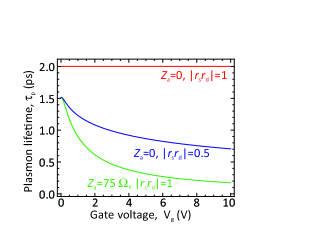
The two latter contributions to damping rate are minimized in the vicinity of charge neutrality point. Examples of calculated plasmon lifetime including the contributions of contacts and antenna are shown in Supplementary Fig. 6. Effects of radiative contribution to plasmon damping on detector responsivity is shown in Supplementary Note 9, along with the discussion of detection mechanisms.
As the wave vector at fixed frequency is inversely proportional to wave velocity, , expression (23) can be transformed to the voltage scale
| (27) |
Supplementary Note 8: Photothermoelectric rectification in Fabri-Perot cavity
Asymmteric feeding of THz radiation results in asymmetric heating of the device and emergence of thermoelectric effect. The resulting dc voltage is Bandurin2017
| (28) |
where is the Seebeck coefficient in the gated channel, and – in the metal-doped graphene contact, is the local temperature at the source junction and is at the drain junction . From now on, we refer to the gated part of graphene as ”channel” and ungated part – as ”contact”. The doping of ungated part does not depend on gate voltage, however, it can be non-uniform due to the effects of built-in field near metal contacts.
The temperature difference induced by non-uniform heating of the device can be found from the solution of heat transfer equation in the channel:
| (29) |
where is the Joule heating power, is the electron thermal conductivity in the channel, is the thermal relaxation length, is the energy relaxation time due to heat sink into substrate phonons Low2012 , and is the heat capacitance of the electronic system. Equation (29) is supplemented by the boundary conditions at the boundaries of gated domain
| (31) |
these conditions follow from the continuity of heat flux at the interfaces. The sought-for temperature difference between source and drain can be obtained in the closed form under the following simplifying assumptions (1) the Joule heating occurs only in the channel (2) the temperature drop across the contacts is much less than maximum overheating in the channel. Both conditions are justified by the small length of the contacts . Under these assumptions, the expression for the photo-thermoelectric voltage acquires a physically appealing form
| (32) |
The quantity is the thermal conductance of the contact, while the integral is the difference of heat fluxes traveling toward the source and toward the drain. The kernel of the integral is anti-symmetric with respect to the middle of the channel , therefore, the PTE signal appears only due to asymmetric heating . Final evaluation of PTE voltage is performed by substituting the solution for electric field (12) into (32):
| (33) |
where .
Supplementary Note 9: Dyakonov-Shur rectification in Fabri-Perot cavity
The so-called Dyakonov-Shur rectification includes two physically different nonlinearities. One contribution to the rectified current appears due to simultaneous modulation of 2d channel conductivity and application of longitudinal field. This effect, also known as resistive self-mixing, results in the rectified voltage
| (34) |
Here is the dc conductivity of a 2D channel, is the carrier density, and are the elementary charge and effective mass of charge carriers respectively, is the momentum relaxation time, and is the high-frequency conductivity. Evaluation of the integral leads us to the result
| (35) |
Another contribution to rectified voltage stems from the difference of kinetic energies of electron fluid at the source and drain side (Bernoulli law). The underlying nonlinearity is manifested by convective term in the Euler equation for electron fluid Dyakonov1996a . The corresponding rectified voltage is
| (36) |
where is the complex amplitude of high-frequency longitudinal field in the channel given by (12). Using the result for electric field (12), we find
| (37) |
Equations (35) and (37) generalize the known results of Dyakonov and Shur for arbitrary loading of the plasmonic FET at the terminals. Naturally, they reduce to the result of Ref. (3) for high-impedance drain load , yielding the photovoltage given by:
| (38) |
The factor in square brackets peaks when the length of the FET channel matches odd multiples of the plasmon quarter-wavelength.
We note that Eqs. (35), (37) and (38) diverge as the dc gate voltage tends to zero. In fact, this divergence stems from the gradual-channel approximation, relating carrier density and gate voltage , that fails near the charge neutrality point. The account of ambipolar transport involving electrons and holes leads to a simple replacement in Eqs. (35), (37) and (38):
| (39) |
where and are electron and hole densities, and are their effective masses, and is the plasma wave velocity in ambipolar system.
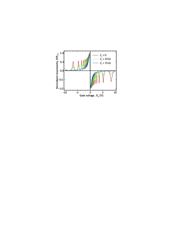
In the main text, the experimental photoresponse was compared with the DS photovoltage from eq. (38) corrected by eq. (39). The full picture of calculated Dyakonov-Shur photovoltage vs gate voltage is shown in Supplementary Fig. 7. Along with the result for perfect reflection from the drain and ideal voltage source (, red line), it also shows the effect of finite antenna impedance on resonance width (green and blue lines). In accordance with the discussed antenna-induced ”renormalization” of input voltage, eq. 13, the resonances at high carrier density are highly broadened due to finite . The width of resonances at low density, on the contrary, is mainly determined by momentum relaxation time.
Supplementary Note 10: Detector operation outside the linear regime
The data reported in the main text were obtained in the regime where the detector’s photovoltage grew linearly with the power of incoming radiation. With increasing outside the linear regime, the heating of graphene’s electronic system by high-frequency ac capacitive currents flowing between the source and gate terminals may affect the resulting responsivity. In order to reveal the role of heating, we have studied the response of our detectors at varying and found that outside the linear regime, decreases with increasing . We attribute this decrease to the modification of the channel conductivity with increasing electronic temperature. To support this statement, we plot the FET-factor obtained by measuring the sample’s conductivity at different inside the sample chamber. Clearly, acquired at different follows the evolution of the FET-factor with . This is reflected in the shift and decrease of the responsivity extrema with increasing . We also refer to Fig. 2a of the main text which shows at different that resembles the behaviour shown in Supplementary Fig. 8.