Corresponding author: c.baker3@uq.edu.au††thanks: CGB and CB contributed equally
Corresponding author: c.baker3@uq.edu.au
Free spectral range electrical tuning of a high quality on-chip microcavity
Abstract
Reconfigurable photonic circuits have applications ranging from next-generation computer architectures to quantum networks, coherent radar and optical metamaterials. However, complete reconfigurability is only currently practical on millimetre-scale device footprints. Here, we overcome this barrier by developing an on-chip high quality microcavity with resonances that can be electrically tuned across a full free spectral range (FSR). FSR tuning allows resonance with any source or emitter, or between any number of networked microcavities. We achieve it by integrating nanoelectronic actuation with strong optomechanical interactions that create a highly strain-dependent effective refractive index. This allows low voltages and sub-nanowatt power consumption. We demonstrate a basic reconfigurable photonic network, bringing the microcavity into resonance with an arbitrary mode of a microtoroidal optical cavity across a telecommunications fibre link. Our results have applications beyond photonic circuits, including widely tuneable integrated lasers, reconfigurable optical filters for telecommunications and astronomy, and on-chip sensor networks.
Dynamically reconfigurable photonic circuits are expected to have a rich variety of applications. For instance, enabling high-bandwidth optical interconnects and memories in next generation computer architectures Atabaki et al. (2018); Kuramochi et al. (2014), chip-based quantum networks Konoike et al. (2016); Elshaari et al. (2017); Aoki et al. (2006), and on-chip coherent radar and microwave communication systems Ghelfi et al. (2014); Xue et al. (2018); Zhuang et al. (2007). Widely tuneable high quality microcavities are a key component for such circuits. Their passive response allows controllable optical phase shifts Zhuang et al. (2007), memories Kuramochi et al. (2014) and add-drop filters Klein et al. (2005) which together provide the reconfigurability of the circuit; while their strong optical confinement enhances light-matter interactions and thereby enables components such as lasers Polman et al. (2004); Li et al. (2013), sensors Lu et al. (2011); Li et al. (2014); Forstner et al. (2014); Heylman et al. (2017), optical frequency combs Del Haye et al. (2007), and quantum processors Aoki et al. (2006).
Full reconfigurability requires that the optical resonance frequencies of each microcavity are tuneable over at least half a free spectral range (FSR), since this allows the interaction of any two spectrally narrow components regardless of their initial frequencies. It is then possible to envisage not only fully-reconfigurable photonic circuits, but also arrays of microcavities forming dynamically controlled optical metamaterials Shalaev (2007) or on-chip microsensor networks Iqbal et al. (2010), and to study collective phenomena such as phase-transitions and topological behaviour in networks of strongly interacting nonlinear photonic systems Heinrich et al. (2011); Douglas et al. (2015); Gil-Santos et al. (2017). Furthermore, FSR tuneable microcavities have many other possible applications. For example, they could allow widely tuneable on-chip lasers Polman et al. (2004); Li et al. (2013), resonant coupling of arbitrary microcavity modes to low-linewidth solid-state and fibre laser sources, reconfigurable filters for background rejection and spectroscopic measurements in astronomy Ellis et al. (2017), matching of cavity resonance frequencies to narrow atomic resonances in cavity quantum electrodynamics Aoki et al. (2006), and stabilisation of on-chip optical frequency combs Del Haye et al. (2007). Despite this range of applications, it has proved challenging to achieve full FSR tuning in a manner that is scalable and allows sub-millimetre device footprints. Approaches demonstrated to-date would require either raising the microcavity to a prohibitively high temperature Armani et al. (2004) or straining it more than is possible with standard piezoelectric materials Jin et al. (2018); Nguyen et al. (2017).
Here we address this challenge, reporting electrical FSR tuning of a high quality silicon chip-based optical microcavity. The key advance is to combine strong nanoelectronic actuation with an engineered microcavity structure that exhibits a highly strain-dependent effective refractive index. The effective refractive index is engineered using the strong optomechanical interaction provided by a double-disk microcavity Rosenberg et al. (2009); Wiederhecker et al. (2009). Hybridisation of the modes of the disks creates an effective index that is strongly dependent on the disk separation, which itself is controlled via electrostatic actuation provided by integrated interdigitated capacitors. Using this approach, we demonstrate the ability to tune optical resonances by up to 9 GHz/V2. This allows FSR tuning with applied voltages of less than 15 V, and a full tuning range in excess of three FSRs. Our devices are fabricated from silica-on-silicon, offering a wide transparency window across and beyond the telecommunications band, but could easily be transferred to other materials such as silicon nitride, silicon-on-insulator, or complementary metal-oxide-semiconductor (CMOS) Atabaki et al. (2018). Capacitive actuation facilitates ultralow power operation, compatible with scalable photonic circuits — the microcavity can be held resonant at any frequency within the silica transparency window using less than a nanowatt of electrical power. To demonstrate the broad-tuning capabilities, we implement a simple two microcavity reconfigurable photonic network, showing that the double-disk microcavity can be brought into resonance with an arbitrary fixed-frequency microtoroidal optical cavity across a telecommunications fibre link.
Background
Most techniques which enable broad tuning of optical cavities can be sorted into two categories. The first applies heat to the cavity through a laser Zhang et al. (2012), metal probe (Armani et al., 2004) or integrated microheater Klein et al. (2005); Lee et al. (2017). This causes a change in temperature of the cavity which modifies its effective refractive index through the thermo-optic effect. The second utilises strain caused by an applied force to deform the boundary of the cavity Sumetsky et al. (2010); Pöllinger et al. (2009). To date, full FSR tuning has not proved possible on sub-millimeter footprints using either of these approaches, although millimeter-scale on-chip silicon-nitride ring resonators have recently been reported with FSR strain tuning provided by an integrated piezoelectric element Jin et al. (2018). In an alternative approach, FSR tuning has been reported with a split-ring microcavity Chu and Hane (2014), consisting of two evanescently coupled curved waveguides. In this case, physically splitting the cavity allows increased mechanical compliance and therefore improved tunability, but introduces inherently large losses that strongly limit the optical quality factor.
In general, the resonance condition of an optical cavity of round-trip physical length requires the optical path length to be an integer multiple of the free space wavelength :
| (1) |
where is the effective refractive index of the cavity. FSR tuning to an adjacent longitudinal mode of the cavity () requires the optical path length to be modified by the free space wavelength. Heat based tuning accomplishes this through a change in the effective refractive index , while strain based tuning changes the physical size of the cavity, where is the resultant strain from the applied force. From Eq. 1, these tuning mechanisms result directly in the conditions for FSR tuning:
| (2) |
The inverse cavity length scaling present in both cases explains why it is highly challenging to achieve FSR tuning for microscale cavities. For instance, tuning a silica disk with radius m by an FSR would require upwards of 200∘C, or a radial strain of , exceeding the maximum strain of common piezoelectric materials such as PZT (lead zirconium titanate) Nguyen et al. (2017) (see supplementary information for more information). Moreover, heat-based tuning suffers from two additional drawbacks, namely typically slow thermal response times and power consumption typically upwards of several milliwatts per device to achieve and maintain the large temperature increases required for significant tuning (Lee et al., 2017). Alternatively, refractive-index tuning could be achieved by electro-optic techniques with materials such as lithium niobate. However, while these enable ultrafast modulation rates up to tens of Gb/s Chen et al. (2014); Wang et al. (2018), they typically allow for much smaller tuning ranges of only a few optical linewidths, so are not included further in this discussion.
In this work, we overcome this miniaturization bottleneck with a technique which brings FSR-tuning capabilities to high quality microscale devices. Whereas most thermal-based approaches rely on changing the effective refractive index through the material’s thermo-optic coefficient, and most strain-based approaches rely on changing the cavity length (see Eq. 1), it is possible to use the optomechanical interaction to engineer an effective refractive index which is very strongly strain-dependent, much beyond the intrinsic photoelastic properties of the material Baker et al. (2014); Balram et al. (2014). This allows far greater tunability to be observed than that achievable through simple physical compression of the cavity.
Double-disk geometry
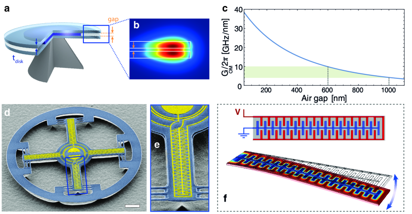
Previous approaches to refractive index engineering have typically involved bringing an external dielectric into the near-field of the cavity Errando-Herranz et al. (2015). Here we achieve greatly enhanced refractive index shifts by engineering the strain to modulate the coupling between two optical resonances. As an additional advantage, in this configuration any scattered light is preferentially scattered back into the optical supermode formed by the coupled cavities. This minimises energy loss when compared with the introduction of an external dielectric. We employ a double-disk Whispering Gallery Mode (WGM) geometry, previously reported by several groups (Wiederhecker et al., 2009; Jiang et al., 2009; Lin et al., 2009; Rosenberg et al., 2009; Wiederhecker et al., 2011; Zhang et al., 2012). Such a cavity consists of two several-hundred-nanometer thick stacked disks, separated by a thin sacrificial layer which is etched-out to leave an air gap (Fig. 1(a)). The optical field is shared between both disks in a supermode, with a significant part of the energy situated in the gap (Fig. 1(b)). This makes the resonance wavelength very sensitive to changes in the separation between the disks, which corresponds to a large optomechanical coupling strength Aspelmeyer et al. (2014), see Fig. 1(c). This large coupling strength, combined with the much greater compliance of the disk resonators to out-of-plane deflection rather than purely radial compressive strain111To estimate this, we can compare the typical mechanical resonance frequency of the radial breathing mode (tens of MHz) for devices of this size to that of the out-of-plane flexural mode (tens of kHz). With the spring constant scaling as , this gives roughly six orders of magnitude larger compliance., allows for the use of much smaller forces to tune the device. For example, even the optical gradient force (radiation pressure) due to circulating power in the resonator can be used to achieve significant tuning of the optical resonance frequency Rosenberg et al. (2009); Thourhout and Roels (2010), including full FSR tunability Wiederhecker et al. (2011). With this purely optical tuning technique, however, a several milliwatt widely tunable pump laser is required for every microcavity to achieve and maintain the desired resonance frequency. The need for multiple tunable lasers, and associated power consumption, precludes use in a scalable photonic network or circuit. Here, instead, we apply tuning forces by integrating interdigitated capacitive electrodes with sub-micron characteristic dimensions onto the surface of the cavity. This provides a direct, scalable and low power electronic tuning mechanism.
I Results
Fabrication and device design
Figure 1(d) shows a SEM top-view of a fabricated double-disk electro-optomechanical cavity. Devices are fabricated from a wafer containing two silica (SiO2) layers with nominal thickness nm separated by an amorphous silicon (-Si) sacrificial layer of nominal thickness 300 nm, grown by ICP-CVD atop a silicon substrate, see Fig. 1(a). We use reactive ion etching to etch through the three-layer stack (SiO2/-Si/SiO2) with an electron-beam lithography (EBL)-defined pattern in the shape of an annulus supported by four wide spokes. We release the device through removal of the -Si sacrificial layer with a XeF2 isotropic dry etch. The released annuli confine light in WGM resonances and have outer diameter of 180 m; more than a factor of six smaller than the smallest previous high quality FSR-tunable on-chip cavity Jin et al. (2018). Thin tethers are included at the point of attachment of the spokes with the annulus to minimize buckling effects due to residual compressive stress in the silica layers coming from the deposition process. Gold sub-micron interdigitated electrodes (500 nm width and spacing) are patterned on the top disk, covering the surface of the support spokes (see Fig. 1(e)). The top and bottom disks are free to move independently, effectively modulating the air gap distance and the structure’s effective refractive index in response to a voltage bias on the drive electrodes. We choose this design as a compromise that provides large available area to deposit electrodes for capacitive driving and minimizes buckling effects (see supplementary information for more details and full process flow). We note that the design can be modified to include integrated optical waveguides Baker et al. (2011) and electrical bridges to the contact pads Lee et al. (2017), to enable fully on-chip packaging. We also note that the capacitive tuning method presented here is quite general and material agnostic. It would work with any combination of optically transparent and sacrificial layer materials such as GaAs/AlGaAs, Si/SiO2, SiN/SiO2 or SiN/Si, and is CMOS compatible.
Modelling of capacitive tuning
For capacitive tuning, and assuming linear mechanical response, the optical frequency shift of the cavity is given by , where the optical tunability can be expressed as:
| (3) |
Here, the mechanical tunability is a measure of the physical compliance of the structure times the efficiency of the capacitive actuation along the vertical direction, with the spring constant of the structure. The mechanical tunability quantifies the physical change in disk separation in response to an applied voltage, with the total deflection in the vertical direction given by , where the applied capacitive force .
In order to estimate the mechanical tunability of the double-disk cavity, we make the simplifying assumption that any vertical motion of the support spokes will be transferred directly to the outer annulus, thereby changing the separation of the disks. In this approximation, the mechanical tunability of the entire device is equal to that of the individual spokes. We therefore seek to quantify how the spokes react to a voltage applied on the interdigitated electrodes. Since the response to an applied voltage involves not only uniaxial compression of the spoke, but also significant out-of-plane deflection and change in the spoke’s curvature, the analytical estimation of is non-trivial. For this reason, we perform 3D Finite Element Method (FEM) electromechanical simulations (see Fig. 1(f)) to calculate the new equilibrium position of the spoke with an applied voltage bias. These predict a mechanical tunability of the support spokes on the order of 1 nm/V2.
To quantify the optomechanical coupling strength for a given disk thickness we need only to know the size of the air gap between the disks. Due to variation in material stress and conditions during fabrication, the gap size was experimentally found to vary over several hundred nanometers. In Figure 1(c) the typical range of disk separations observed after fabrication is shown, with a corresponding range of coupling strengths of GHz/nm. Combined with the predicted mechanical tunability, Eq. 3 yields a range of predicted optical tunabilities of GHz/V2 (see supplementary material for more information). For a double-disk structure of 90 m outer radius, this predicts FSR tuning to be easily achievable with applied voltages of less than 15 V.
These predictions indicate that refractive index engineering along with interdigitated capacitors can overcome the scaling bottleneck for resonator tuning, allowing electrical FSR tuning of microscale devices. It is notable, however, that they are far from the ultimate limit of this technique. With further optimisation of both the double-disk geometry and capacitive actuation, the device radius could be reduced to below 15 m while maintaining FSR-tuning capability with an applied voltage of less than 15 V (see supplementary information). We note that piezoelectric actuation, such as utilised in the work of Jin, et al.Jin et al. (2018), could be used as an alternative to interdigitated capacitors. Based on our predictions, capacitive actuation, beyond the advantage of requiring only a single deposition step to fabricate, interestingly also provides more efficient tuning for devices at the scale of tens of microns (see supplementary information).
Free spectral range tuning
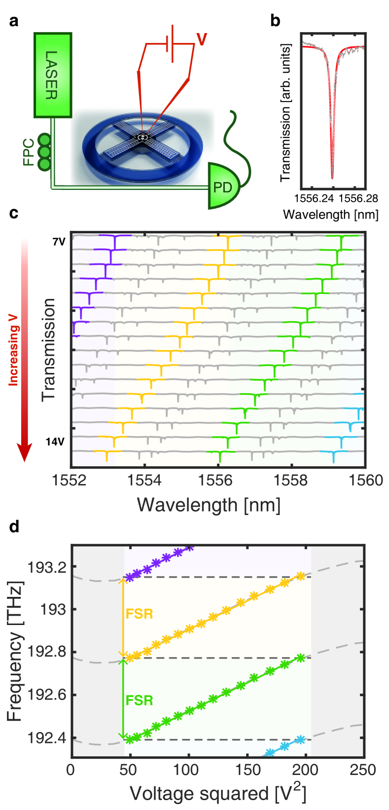
Figure 2(a) shows a schematic of the experimental setup. Light is evanescently coupled to the double-disk through a tapered optical fibre. Spectroscopy of the devices is performed with a tunable diode laser (Yenista T100S-HP). The two interdigitated electrodes are contacted using ultrasharp tungsten probe tips, which are connected to a DC voltage source. (See supplementary information for more details.) Figure 2(b) shows a typical optical resonance of a device, measured by sweeping the laser frequency rapidly over the resonance, yielding an intrinsic optical quality factor of .
Figure 2(c) displays a series of successive optical transmission spectra of a device as the WGMs of the device are tuned across an entire FSR. Consecutive traces from top to bottom are acquired as the voltage is ramped up by steps of 0.5 V, starting from V, with full FSR tuning achieved at V. We observe that the optical quality factor of the modes remain unperturbed throughout the entire tuning range. Next, the frequencies of the four highlighted WGMs in Fig. 2(c) are tracked versus , in order to extract the optical tunability . These results are shown in Fig. 2(d). In the region [50; 200], corresponding to the voltage range [7; 14] shown in Fig. 2(c), we observe a linear trend, with a slope of GHz/V2. Comparable tuning is found in other devices of a similar design, with a maximum observed tunability of 9 GHz/V2 and tuning ranges exceeding three free spectral ranges (see supplementary information). These results are in line with the predictions from the simulations outlined above, where uncertainty in the disk separation led to a prediction of GHz/V2 . In addition to the expected scaling, further evidence that the tuning is capacitive in nature (and not for instance due to electrostatic interactions between the top disk electrodes and trapped charges on the bottom disk) is provided by observing that the tuning has the same direction with a positive e.g. (0; +10 V) as with a negative e.g. (0; -10 V) bias applied to the electrodes.
Outside of the range [7; 14], the relationship between frequency shift and the square of the applied voltage departs from linearity, implying a changing optical tunability. We ascribe this behaviour to nonlinearities in the mechanical response due to out-of-plane warping of the double-disk due to residual stress in the silica layers, as confirmed by optical profilometry measurements222We note here interestingly that SEM measurements cannot be relied on for accurate measurements of the disks’ geometry and separation, because the significant charging brought about by the electron beam creates strong electrostatic forces that modify the disk separation and can cause collapse of the double-disk structure. of the fabricated double-disks (see supplementary materials). This warping causes mechanical buckling transitions which modify the mechanical compliance, sometimes with clear steps in the optical tunability (see supplements).
As well as allowing full FSR tunability, a second key feature of the capacitive tuning presented in this paper is its ultra-low power consumption. In contrast to thermal tuning techniques which require the heating to be maintained as long as the wavelength offset is required, here the only power required to maintain a wavelength offset is that dissipated through leakage current in the electrodes. We measure a leakage current of 2 pA per Volt applied to the electrodes, corresponding to a leakage/parasitic resistance of 500 G. With an applied voltage of V required to maintain full FSR tuning, this parasitic resistance results in a power consumption of 400 pW. This ultralow power consumption makes our approach particularly scalable.
Demonstration of a basic reconfigurable photonic network
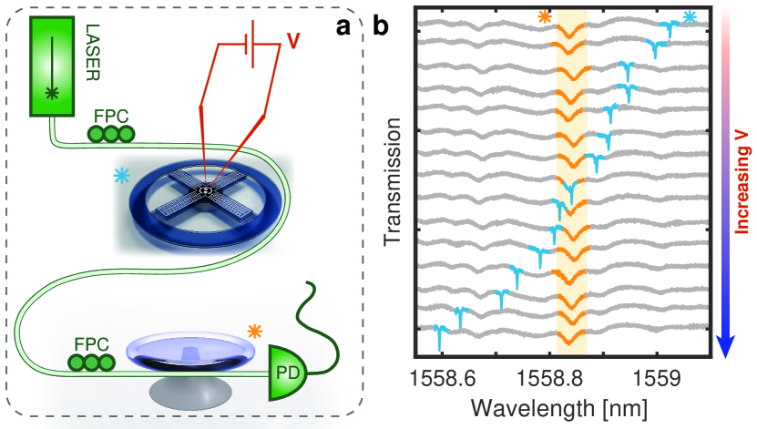
As a demonstration of the capability of full FSR microcavity tuning, we employ it in a simple reconfigurable photonic network. In this network, a tunable double-disk cavity is coupled to an arbitrary optical mode of a passive microtoroidal cavity through a telecommunications optical fibre link, as shown in Fig. 3(a). Initially, the optical resonances of the two devices are far separated in frequency, as seen in the top trace of Fig. 3(b). Indeed, two resonators taken at random have very low chances of sharing a common resonance, particularly as devices dimensions are scaled down and for high optical quality factors, with the odds scaling as the reciprocal of the product of their finesses. The resonance of the microtoroid remains static, determined by its geometry, while applying a voltage to the double-disk allows it to be tuned into resonance with the toroid. This allows for switching between interacting and non-interacting cavities at will Zhang et al. (2012); Lee et al. (2017), but also mimics the coupling of arrays of dissimilar cavities for optical networks or optomechanical synchronization Gil-Santos et al. (2017); Zhang et al. (2012), the tuning of a cavity to an atomic transition in cavity QED Aoki et al. (2006), or the coupling of a resonator to a fixed-wavelength laser source.
II Discussion
We have reported full FSR electrical tuning of a high quality silicon chip-based optical microcavity. To achieve this we develop a new approach to FSR tuning, combining engineering of the optomechanical interaction to create a highly strain-dependent effective refractive index with electrical actuation through integrated interdigitated capacitors. This approach overcomes a key bottleneck for nanophotonic circuit-compatible FSR tuning, avoiding the need to locally raise the microcavity temperature by hundreds of degrees Armani et al. (2004) or apply strains larger than are available from standard piezoelectric materials Jin et al. (2018); Nguyen et al. (2017). We demonstrate frequency tuning over more than three FSRs, with tuning over an FSR requiring applied voltages of less than 15 V. Less than a nanowatt of electrical power is needed to sustain an FSR frequency shift, compatible with the densely packed arrays of microresonators proposed for next generation computer architectures Atabaki et al. (2018). Our devices are fabricated from silica-on-silicon allowing arbitrary resonance frequency tuning across the full silica transparency window. They could be translated straightforwardly into other material platforms, such as silicon nitride, silicon-on-insulator and CMOS depending on application Atabaki et al. (2018). To illustrate the capabilities of full FSR tuning, we demonstrate a two microcavity reconfigurable photonic network consisting of one FSR tunable device brought on resonance with a fixed-frequency microtoroidal cavity across a telecommunications optical fibre link.
We expect that full FSR electrical tuning of high quality optical microcavities will enable a broad range of science and applications, from high-bandwidth optical interconnects and memories in next generation computer architectures Atabaki et al. (2018); Kuramochi et al. (2014), to on-chip tuneable filters, lasers and coherent radar systems Ellis et al. (2017); Polman et al. (2004); Li et al. (2013); Ghelfi et al. (2014); Xue et al. (2018); Zhuang et al. (2007), reconfigurable sensor networks Iqbal et al. (2010), quantum networks Konoike et al. (2016); Elshaari et al. (2017); Aoki et al. (2006), and arrays of nonlinear photonic systems to study collective phenomena such as phase transitions and topological behavior Heinrich et al. (2011); Douglas et al. (2015); Gil-Santos et al. (2017).
References
- Atabaki et al. (2018) A. H. Atabaki, S. Moazeni, F. Pavanello, H. Gevorgyan, J. Notaros, L. Alloatti, M. T. Wade, C. Sun, S. A. Kruger, H. Meng, et al., Nature 556, 349 (2018).
- Kuramochi et al. (2014) E. Kuramochi, K. Nozaki, A. Shinya, K. Takeda, T. Sato, S. Matsuo, H. Taniyama, H. Sumikura, and M. Notomi, Nature Photonics 8, 474 (2014).
- Konoike et al. (2016) R. Konoike, H. Nakagawa, M. Nakadai, T. Asano, Y. Tanaka, and S. Noda, Science advances 2, e1501690 (2016).
- Elshaari et al. (2017) A. W. Elshaari, I. E. Zadeh, A. Fognini, M. E. Reimer, D. Dalacu, P. J. Poole, V. Zwiller, and K. D. Jöns, Nature communications 8, 379 (2017).
- Aoki et al. (2006) T. Aoki, B. Dayan, E. Wilcut, W. P. Bowen, A. S. Parkins, T. J. Kippenberg, K. J. Vahala, and H. J. Kimble, Nature 443, 671 (2006).
- Ghelfi et al. (2014) P. Ghelfi, F. Laghezza, F. Scotti, G. Serafino, A. Capria, S. Pinna, D. Onori, C. Porzi, M. Scaffardi, A. Malacarne, et al., Nature 507, 341 (2014).
- Xue et al. (2018) X. Xue, Y. Xuan, C. Bao, S. Li, X. Zheng, B. Zhou, M. Qi, and A. M. Weiner, Journal of Lightwave Technology 36, 2312 (2018).
- Zhuang et al. (2007) L. Zhuang, C. Roeloffzen, R. Heideman, A. Borreman, A. Meijerink, and W. van Etten, IEEE Photonics Technology Letters 19, 1130 (2007).
- Klein et al. (2005) E. J. Klein, D. H. Geuzebroek, H. Kelderman, G. Sengo, N. Baker, and A. Driessen, IEEE Photonics Technology Letters 17, 2358 (2005).
- Polman et al. (2004) A. Polman, B. Min, J. Kalkman, T. Kippenberg, and K. Vahala, Applied Physics Letters 84, 1037 (2004).
- Li et al. (2013) B.-B. Li, Y.-F. Xiao, M.-Y. Yan, W. R. Clements, and Q. Gong, Optics letters 38, 1802 (2013).
- Lu et al. (2011) T. Lu, H. Lee, T. Chen, S. Herchak, J.-H. Kim, S. E. Fraser, R. C. Flagan, and K. Vahala, Proceedings of the National Academy of Sciences 108, 5976 (2011).
- Li et al. (2014) B.-B. Li, W. R. Clements, X.-C. Yu, K. Shi, Q. Gong, and Y.-F. Xiao, Proceedings of the National Academy of Sciences 111, 14657 (2014).
- Forstner et al. (2014) S. Forstner, E. Sheridan, J. Knittel, C. L. Humphreys, G. A. Brawley, H. Rubinsztein-Dunlop, and W. P. Bowen, Advanced materials 26, 6348 (2014).
- Heylman et al. (2017) K. D. Heylman, K. A. Knapper, E. H. Horak, M. T. Rea, S. K. Vanga, and R. H. Goldsmith, Advanced Materials , 1700037 (2017).
- Del Haye et al. (2007) P. Del Haye, A. Schliesser, O. Arcizet, T. Wilken, R. Holzwarth, and T. J. Kippenberg, Nature 450, 1214 (2007).
- Shalaev (2007) V. M. Shalaev, Nature photonics 1, 41 (2007).
- Iqbal et al. (2010) M. Iqbal, M. A. Gleeson, B. Spaugh, F. Tybor, W. G. Gunn, M. Hochberg, T. Baehr-Jones, R. C. Bailey, and L. C. Gunn, IEEE Journal of Selected Topics in Quantum Electronics 16, 654 (2010).
- Heinrich et al. (2011) G. Heinrich, M. Ludwig, J. Qian, B. Kubala, and F. Marquardt, Physical review letters 107, 043603 (2011).
- Douglas et al. (2015) J. S. Douglas, H. Habibian, C.-L. Hung, A. Gorshkov, H. J. Kimble, and D. E. Chang, Nature Photonics 9, 326 (2015).
- Gil-Santos et al. (2017) E. Gil-Santos, M. Labousse, C. Baker, A. Goetschy, W. Hease, C. Gomez, A. Lemaître, G. Leo, C. Ciuti, and I. Favero, Physical Review Letters 118, 063605 (2017).
- Ellis et al. (2017) S. C. Ellis, S. Kuhlmann, K. Kuehn, H. Spinka, D. Underwood, R. R. Gupta, L. E. Ocola, P. Liu, G. Wei, N. P. Stern, J. Bland-Hawthorn, and P. Tuthill, Optics Express 25, 15868 (2017).
- Armani et al. (2004) D. Armani, B. Min, A. Martin, and K. J. Vahala, Applied Physics Letters 85, 5439 (2004).
- Jin et al. (2018) W. Jin, R. G. Polcawich, P. A. Morton, and J. E. Bowers, Opt. Express, OE 26, 3174 (2018).
- Nguyen et al. (2017) M. D. Nguyen, E. P. Houwman, and G. Rijnders, Scientific Reports 7, 12915 (2017).
- Ding et al. (2010) L. Ding, C. Baker, P. Senellart, A. Lemaitre, S. Ducci, G. Leo, and I. Favero, Physical Review Letters 105 (2010), 10.1103/PhysRevLett.105.263903.
- Lin et al. (2009) Q. Lin, J. Rosenberg, X. Jiang, K. J. Vahala, and O. Painter, Phys. Rev. Lett. 103, 103601 (2009).
- Baker et al. (2016) C. G. Baker, C. Bekker, D. L. McAuslan, E. Sheridan, and W. P. Bowen, Optics Express 24, 20400 (2016).
- Bekker et al. (2017) C. Bekker, R. Kalra, C. Baker, and W. P. Bowen, OPTICA 4, 1196 (2017).
- Rosenberg et al. (2009) J. Rosenberg, Q. Lin, and O. Painter, Nature Photonics 3, 478 (2009).
- Wiederhecker et al. (2009) G. S. Wiederhecker, L. Chen, A. Gondarenko, and M. Lipson, nature 462, 633 (2009).
- Zhang et al. (2012) M. Zhang, G. S. Wiederhecker, S. Manipatruni, A. Barnard, P. McEuen, and M. Lipson, Physical Review Letters 109, 233906 (2012).
- Lee et al. (2017) B. S. Lee, M. Zhang, F. A. S. Barbosa, S. A. Miller, A. Mohanty, R. St-Gelais, and M. Lipson, Opt. Express 25, 12109 (2017).
- Sumetsky et al. (2010) M. Sumetsky, Y. Dulashko, and R. S. Windeler, Optics letters 35, 1866 (2010).
- Pöllinger et al. (2009) M. Pöllinger, D. O’Shea, F. Warken, and A. Rauschenbeutel, Physical Review Letters 103, 053901 (2009).
- Chu and Hane (2014) H. M. Chu and K. Hane, IEEE Photonics Technology Letters 26, 1411 (2014).
- Chen et al. (2014) L. Chen, Q. Xu, M. G. Wood, and R. M. Reano, Optica 1, 112 (2014).
- Wang et al. (2018) C. Wang, M. Zhang, B. Stern, M. Lipson, and M. Lončar, Optics Express 26, 1547 (2018).
- Baker et al. (2014) C. Baker, W. Hease, D.-T. Nguyen, A. Andronico, S. Ducci, G. Leo, and I. Favero, Optics Express 22, 14072 (2014).
- Balram et al. (2014) K. C. Balram, M. Davanço, J. Y. Lim, J. D. Song, and K. Srinivasan, Optica 1, 414 (2014).
- Errando-Herranz et al. (2015) C. Errando-Herranz, F. Niklaus, G. Stemme, and K. B. Gylfason, Optics Letters 40, 3556 (2015).
- Jiang et al. (2009) X. Jiang, Q. Lin, J. Rosenberg, K. Vahala, and O. Painter, Opt. Express, OE 17, 20911 (2009).
- Wiederhecker et al. (2011) G. S. Wiederhecker, S. Manipatruni, S. Lee, and M. Lipson, Optics Express 19, 2782 (2011).
- Aspelmeyer et al. (2014) M. Aspelmeyer, T. J. Kippenberg, and F. Marquardt, Reviews of Modern Physics 86, 1391 (2014).
- Note (1) To estimate this, we can compare the typical mechanical resonance frequency of the radial breathing mode (tens of MHz) for devices of this size to that of the out-of-plane flexural mode (tens of kHz). With the spring constant scaling as , this gives roughly six orders of magnitude larger compliance.
- Thourhout and Roels (2010) D. V. Thourhout and J. Roels, Nature Photonics 4, 211 (2010).
- Baker et al. (2011) C. Baker, C. Belacel, A. Andronico, P. Senellart, A. Lemaitre, E. Galopin, S. Ducci, G. Leo, and I. Favero, Applied Physics Letters 99, 151117 (2011).
- Note (2) We note here interestingly that SEM measurements cannot be relied on for accurate measurements of the disks’ geometry and separation, because the significant charging brought about by the electron beam creates strong electrostatic forces that modify the disk separation and can cause collapse of the double-disk structure.
Acknowledgments This research was primarily funded by the Australian Research Council and Lockheed Martin Corporation through the Australian Research Council Linkage Grant LP140100595. Support was also provided by a Lockheed Martin Corporation seed grant and the Australian Research Council Centre of Research Excellence for Engineered Quantum Systems (CE110001013). W.P.B., C.G.B, R.K. and B.L. acknowledge fellowships from the Australian Research Council (FT140100650) and the University of Queensland (UQFEL1833877 & UQFEL1719237 & UQFEL14001447), respectively. This work was performed in part at the Queensland node of the Australian National Fabrication Facility, a company established under the National Collaborative Research Infrastructure Strategy to provide nano and microfabrication facilities for Australia’s researchers. The authors acknowledge the facilities, and the scientific and technical assistance, of the Australian Microscopy & Microanalysis Research Facility at the Centre for Microscopy and Microanalysis, The University of Queensland. The authors acknowledge Mariusz Martyniuk and Dhirendra Tripathi at the University of Western Australia for the growth of the wafers, as well as Miaoqiang Liu from the Wang group and Daniel Szombati from the Fedorov group at the University of Queensland, for access to equipment and aid in annealing the wafers and depositing the metal layer, respectively.