Charged impurity scattering in two-dimensional materials with ring-shaped valence bands: GaS, GaSe, InS, and InSe
Abstract
The singular density of states and the two Fermi wavevectors resulting from a ring-shaped or “Mexican hat” valence band give rise to unique trends in the charged impurity scattering rates and charged impurity limited mobilities. Ring shaped valence bands are common features of many monolayer and few-layer two-dimensional materials including the III-VI materials GaS, GaSe, InS, and InSe. The wavevector dependence of the screening, calculated within the random phase approximation, is so strong that it is the dominant factor determining the overall trends of the scattering rates and mobilities with respect to temperature and hole density. Charged impurities placed on the substrate and in the 2D channel are considered. The different wavevector dependencies of the bare Coulomb potentials alter the temperature dependence of the mobilities. Moving the charged impurities 5 Å from the center of the channel to the substrate increases the mobility by an order of magnitude.
pacs:
Valid PACS appear hereI Introduction
Atomically thin two-dimensional (2D) materials are being investigated for a range of applications including emerging beyond-CMOS electronic devices, thermoelectrics, and optoelectronics. A number of these materials have “ring-shaped” valence bands. These materials include the semiconducting III-VI monochalcogenides, GaS, GaSe, InS, and InSe darshanamhat ; zolyomi_GaX ; zolyomi_InX ; GaS_photodetector_AnPingHu ; Hennig_GroupIII_ChemMat ; SGLouie_GaSe_arxiv ; WYao_GaS_GaSe_arxiv ; guo2017band , bilayer graphene when subject to a vertical electric field Fermi_ring_Neto_PRB07 ; Falko_BLG_Lifshitz_PRL14 ; MacDonald_bi_gap_PRB07 , monolayers of Bi2Se3darshanamhat and Bi2Te3Zahid_Lake ; Lundstrom_Jesse_Bi2Te3 ; Udo_Bi2Se3 , few-layers of Bi2Se3 intercalated with 3d transition metalsli2016gate , monolayer SnOseixas2016multiferroic ; houssa2017hole , 2D hexagonal lattices of group-VA elements sevinccli2017quartic , and hexagonal group-V binary compoundsnie2017room .
A ring-shaped valence band edge results in a singularity in the 2D density of states and a step function turn on of the density of modes at the valence band edge Lundstrom_Jesse_Bi2Te3 ; darshanamhat ; GaSe_Ajayan_NL13 ; Ajayan_InSe ; GaSe_Geohagen_ACSNano . At low temperatures, density functional theory calculations show that the singularity in the density of states leads to a ferromagnetic phase transition at sufficient hole doping in GaS and GaSeSGLouie_GaSe_arxiv ; WYao_GaS_GaSe_arxiv . More recent calculations find that such a transition is a general property of the Mexican hat dispersion seixas2016multiferroic .
The ring-shaped dispersion affects ionized impurity scattering through the density of states, the momentum transfer required to scatter around the ring, and the momentum dependence of the screening. The question we address is what is the influence of the “ring-shaped” dispersion on the temperature, density, and Fermi energy dependence of the ionized impurity scattering rates and ionized impurity limited mobility.
Prior studies have theoretically investigated the role of ionized impurity scattering in two–dimensional materials with a parabolic dispersion. Ionized impurity scattering can severely limit the mobility in the transition metal dichalcogenides such as MoS2 DJena_PRX and give rise to an unexpected temperature dependence of the mobility ong2013mobility . It has been predicted that reducing the doping can enhance the linear screening response within the Thomas-Fermi theory kolomeisky2016anomalous . The role of screening on charged impurity scattering and charged impurity limited mobility in materials with a ring-shaped dispersion has not yet been addressed.
We address this question using an analytical bandstructure model with parameters extracted from first principles calculation. Screening is included within the random phase approximation. Polarization functions and scattering rates are analyzed, and the ionized impurity limited hole mobility of the III-VI materials, GaS, GaSe, InS, and InSe, are compared.
II Theory
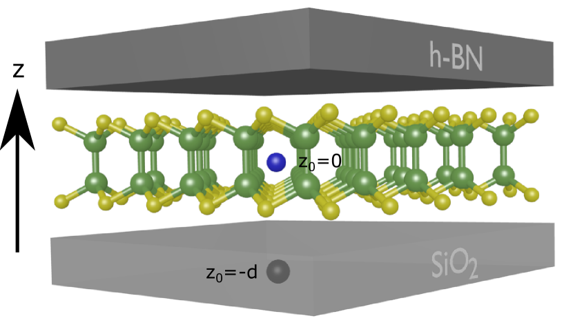
The materials and geometry of the problem consist of a monolayer 2D semiconducting material on a insulating substrate encapsulated by an insulating capping layer which could be the same as the substrate. Example insulating materials are BN or SiO2. The structure is illustrated in Fig. 1 with SiO2 for the substrate and BN for the capping layer. A cylindrical coordinate system is used with a vector in the – plane. The origin is at the center of the semiconductor. Charged impurities will be considered for two different positions, in the center of the 2D semiconductor, , and on the surface of the substrate, . Accounting for the Å thickness of a monolayer III-VI semiconductor and the Å van der Waals gap,darshanamhat we use Å for the charged impurities on the surface of the substrate. The value of the impurity density used in all calculations is cm-2. All calculated scattering rates are linearly proportional to the impurity density, and all mobilities are inversely proportional to the impurity density, so any calculated values can be scaled for different impurity densities.
The investigation of the effect of the Mexican hat dispersion on screening, scattering, and mobility, begins with the model quartic dispersion
| (1) |
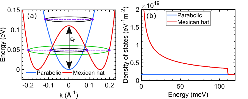
Quartic models have been previously used to investigate interactions in biased bilayer graphene Fermi_ring_Neto_PRB07 , multiferroic 2D materials seixas2016multiferroic , and electronic and thermoelectric properties of group III-VI and group VA 2D materials darshanamhat ; sevinccli2017quartic . We define our momentum-energy relation such that the hole kinetic energy is positive, the valence band edge is at , and negative energies correspond to energies in the band gap. The term in Eq. (1) is the height of the ‘hat’ at and is the magnitude of the effective mass at (the top of the hat). The addition of the constant term in Eq. (1), shifts the dispersion so that the minimum energy, corresponding to the band edge, occurs at . For energies the Mexican hat dispersion has two Fermi wavevectors corresponding to the two branches of the dispersion. In this energy region, the Fermi surface consists of two concentric circles shown in Fig. 2(a). The radii of the two circles are and . At the band edge, , the two circles merge into a single circle with a radius of . The effective mass at the band edge determined from is . The single–spin densities of states for each individual -space ring are identical and equal to
| (2) |
The total single-spin density of states is given by the sum and is equal to
| (3) |
The density of states is plotted in Fig. 2(b) using m0 and eV, which are similar to the values for monolayer GaS darshanamhat . The density of states diverges as at the band edge, and it is equal to the single–spin parabolic density of states, , at the top of the hat.
A parabolic dispersion will be used as a reference and for comparison. The parabolic and Mexican hat dispersions and density of states are plotted together in Fig. 2. An effective mass of is used for both dispersions.
The two–dimensional Fourier transform of the bare Coulomb potential for a point charge at position , is
| (4) |
where is the charge of electron, is the average static dielectric constant and is the momentum transfer. Since all of the III-VI materials have relative dielectric constants in the range of , we will use the dielectric constant of the semiconductor. Within the random phase approximation, the screened Coulomb potential is
| (5) |
Substituting Eq. (4) into Eq. (5) gives the 2D RPA screened potential,
| (6) |
where is the wavevector dependent inverse screening length. In the static limit, the polarization function is maldague1978many
| (7) |
where is the area, is the eigenenergy at wavevector , and is the Fermi-Dirac function. The factor of 2 is for spin degeneracy, since the Mexican hat bands in the III-VI materials are spin degenerate. For both the Mexican hat and parabolic dispersions, is only a function of the magnitude of . Therefore, we define the variable,
| (8) |
and calculate the polarization from Eq. 7,
| (9) |
In the limit , the polarization function becomes the negative of the thermally averaged density of states at the Fermi level,
| (10) |
where is the density of states. Using the limit for in Eq. (6), gives the Thomas-Fermi form of the 2D screened Coulomb potential with an inverse screening length of . For the Mexican hat dispersion this is problematic, since the density of states diverges near the band edge. Note that in defining the polarization function in Eq. (7), .
To calculate the momentum relaxation time, we need the matrix elements of the RPA Coulomb potential. We assume separable wavefunctions of the form and take the matrix elements of to obtain . The Fermi’s golden rule expression for the inverse momentum relaxation time is given by
| (11) |
where is the number of charged impurities. For the Mexican hat dispersion, the group velocity is opposite to the direction of on the inner ring and parallel to on the outer ring. On a given branch of the Mexican hat dispersion, is only a function of the magnitude of . Therefore, by converting the sum over into an integral and explicitly keeping track of the two branches of the dispersion, Eq. (11) becomes
| (12) |
where the sum is over the two Fermi rings, , and correspond to the radii of the concentric iso-energy rings in Fig. 2, is the final single–spin density of states corresponding to ring , is the final group velocity of ring , and is the impurity density per unit area. The value of is either zero for impurities placed at the center of the semiconducting monolayer or Å for impurities placed on the substrate.
The last term on the right of Eq. (11) is where is the angle between the group velocity of state and the group velocity of state . This term is the relative change in the component of the velocity that is parallel to the initial velocity . When the final velocity is in the same direction and greater than the initial velocity , then scattering from to causes the carrier to speed up and gives a negative contribution to the momentum relaxation time 1986_Neg_tau_m . This situation occurs for carriers that are initially near the top of the hat in Fig. 2(a) and then scatter to the outer ring. However, the negative values are restricted to a range of angles centered around , and the integral over in Eq. (12) is always positive.
The carrier mobility is determined from the average group velocity driven by an external electric field oriented in the –direction. To linear order, this is
| (13) |
where is the asymmetric component of the non-equilibrium distribution function. Within the relaxation time approximation, the asymmetric distribution function can be written as,
| (14) |
where is the equilibrium Fermi function, is the electric field along the transport direction and is the direction of with respect to the axis. The mobility is directly evaluated from its definition, . Substituting (14) into (13), the final expression for carrier mobility is
| (15) |
where the spin–degenerate 2D hole density .
III Results
The polarization function gives wavevector dependent screening. In a two dimensional material with parabolic dispersion, the density of states is constant which results in a constant polarization function for at low temperature. In a Mexican hat dispersion, the singular density of states gives a strong wavevector dependence to the polarization function at low temperature. It also increases the overall magnitude of the polarization function. The wavevector dependent inverse screening length is added to the momentum transfer in the denominator of Eq. (6), and the sum determines the magnitude and wavevector dependence of the screened Coulomb interaction. Therefore, we begin by analyzing as a function of for the Mexican hat dispersion.
To provide a point of reference, we first show in Fig. 4(a) the well–known wavevector dependent inverse screening length resulting from a parabolic dispersion with the Fermi level fixed at meV above the band edge. At low temperature and for wavevectors smaller than , the magnitude of is simply , i.e. times the density of states at the Fermi level. This is equal to where is the relative effective mass and is the relative dielectric constant. Since the density of states is constant, the resulting inverse screening length is constant up until the momentum transfer is greater than . At higher temperatures, the polarization function can be written as a convolution of the zero–temperature polarization and a thermal broadening function maldague1978many . The result is that the sharp -dependent features become smeared out at finite temperatures.

Unlike the parabolic dispersion where scattering occurs within a single Fermi ring, Coulomb scattering in a Mexican hat dispersion occurs within and between two concentric rings for energies up to , which defines the height of the Mexican hat dispersion. Furthermore, the density of states is singular at the band edge. To understand the implications of these features, the inverse screening length is plotted, as a function of the momentum transfer, , for different values of the Fermi energy in Fig. 4(b-c) and for a fixed carrier density in Fig. 4(d).
Fig. 4(b) shows the inverse screening length of the Mexican hat dispersion at 3 different temperatures with the Fermi level fixed at meV above the band edge. The low–temperature ( K) curve has a strong dependence that arises from the bandstructure. There are two Fermi wavevectors for denoted as and and illustrated in the inset of Fig. 4(c). The two Fermi wavevectors result in three features for at K. These features correspond to momentum transfers of , , and . Just as with the parabolic dispersion, there is a sharp change in the derivative of when is twice the Fermi wavevector, except now there are two Fermi wavevectors. The third and largest peak occurs when , which is the minimum momentum required to transfer between the two Fermi rings. This can be viewed as a type of Fermi surface nesting. Increasing the temperature smooths out these sharp features, and at K, smoothly decreases with increasing . When the Fermi level is meV below the band edge as in Fig. 4(c), the screening at K is essentially zero since there are no carriers, and the qualitative features of the polarization functions at K and and K are the same as those in Fig. 4(b) with a small reduction in the overall magnitude resulting from the reduced carrier density.
Fig. 4(d) shows the inverse screening lengths at a fixed carrier density of cm-2 for different temperatures. Now, the Fermi level moves with temperature as shown in the legend. At K, the Fermi level is meV above the band edge, and the small peak becomes very large as the Fermi level approaches the singularity in the density of states. At K and K, the Fermi levels are in the band gap, and the polarization functions are similar to those in Fig. 4(c).
Now, we consider the magnitude and angle dependence of the matrix elements of the screened Coulomb potential, given by Eq. (6) with and . Fig. 5 shows polar plots of the screened Coulomb potential with cm-2 at two different temperatures and energies. The polar angle is the angle between and . The relevant plots are shown in Fig. 4(d). For a fixed energy, scattering can occur within the inner ring ( and both lie on the inner ring), within the outer ring ( and both lie on the outer ring), or between the inner ring and the outer ring ( and lie on different rings). These 3 different matrix elements are denoted ‘Inner,’ ‘Outer,’ and ‘Inter,’ respectively, in Fig. 5.
We first consider the low-temperature K matrix elements at an energy of 2.5 meV above the band edge shown in Fig. 5(a). At the carrier density of cm-2, meV, The wavevector dependent screening corresponds to the upper curve in Fig. 4(d), and a more detailed view is shown in Fig. 5(c). At meV, the radius of the inner ring , the radius of the outer ring , and . At , for the inner and outer ring matrix elements and for the inter ring matrix element. At , , and at , . Thus, at , all three scattering mechanisms are strongly suppressed by the screening. The inter ring scattering is a backscattering process, since the two rings have opposite velocities. Thus, the small inter ring backscattering is strongly suppressed by the screening. The values of , and are plotted in Fig. 5(c). The value of in the range of is much larger than . This means that for , the dependence of is determined solely by the dependence of the polarization, and the bare momentum transfer is negligible in comparison.
Since falls rapidly as increases, the RPA screened Coulomb potential in a Mexican hat bandstructure favors large angle scattering. This is opposite to the trend resulting from the bare Coulomb interaction. The large outer-ring matrix elements for between and arise because the momentum transfer around the outer ring becomes larger than . The kink at corresponds to the peak in at . At low temperature, the polarization strongly suppresses the magnitude of the matrix elements at the Fermi level. Only for those energies several above the Fermi level can the momentum transfer become large enough that the polarization becomes negligible, and returns to a dependence. This large momentum transfer corresponds to backscattering across the outer ring.
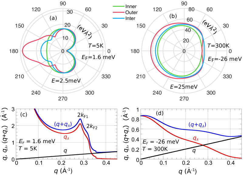
Fig. 5(b) shows the K matrix elements at an energy of 25 meV above the band edge. As the temperature increases to 300 K, both the magnitude and the angular dependence of the matrix elements change considerably compared to those at K. This is a result of the large change in the polarization function as shown in Fig. 4(d). An enlarged view of the K curve is shown in Fig. 5(d). The Fermi level now lies below the band edge at meV. Compared to the K polarization, the magnitude of the polarization decreases by an order of magnitude at the bandedge, the sharp features disappear, and monotonically decreases as increases. However, the overall decrease of over the range of relevant values is relatively small. At meV, and . At , , and at , . Thus, the maximum increase in the matrix element going from to is a factor of , which is shown for the matrix elements of the outer ring in Fig. 5(b). Over the entire range of relevent momentum transfer , the K polarization is much less than the K polarization, so that the matrix elements are uniformly larger at K compared to those at K. Since the scattering rate is proportional to , the scattering rates will be significantly larger at room temperature compared to those at low temperature.
The integrand that determines the momentum scattering rates at a given energy , given by Eq. (12), contains not only , but also the final density of states and the relative change in the velocity which can be positive or negative. The term further reduces the small angle intra-ring matrix elements, which are already small due to the large polarization at small . The integrand of Eq. (12) is plotted in Fig. 6 at K, meV, and meV. Fig. 6(a) shows the angle-dependent scattering rate for the initial on the inner ring, and Fig. 6(b) shows the angle-dependent scattering rate for the initial on the outer ring. Note that the energy meV is meV below the top of the hat in Fig. 2(a). At this energy, the magnitude of the group velocity of a state on the inner ring is much less that of a state on the outer ring. For inter ring scattering from the inner ring to the outer ring, , and a forward scattering process with causes the term in the integrand to become negative. The forward scattering process with corresponds to backscattering in -space with , where is the angle between the initial state on the inner ring and the final state on the outer ring. Thus, in Fig. 6(a), the negative values of , shown by the blue curve, are centered around . Backscattering with corresponds to forward scattering in -space with , and the corresponding positive values of are shown by the red curve centered around . When scattering from the outer ring to the inner ring, , so that is positive for all angles as shown in Fig. 6(b).
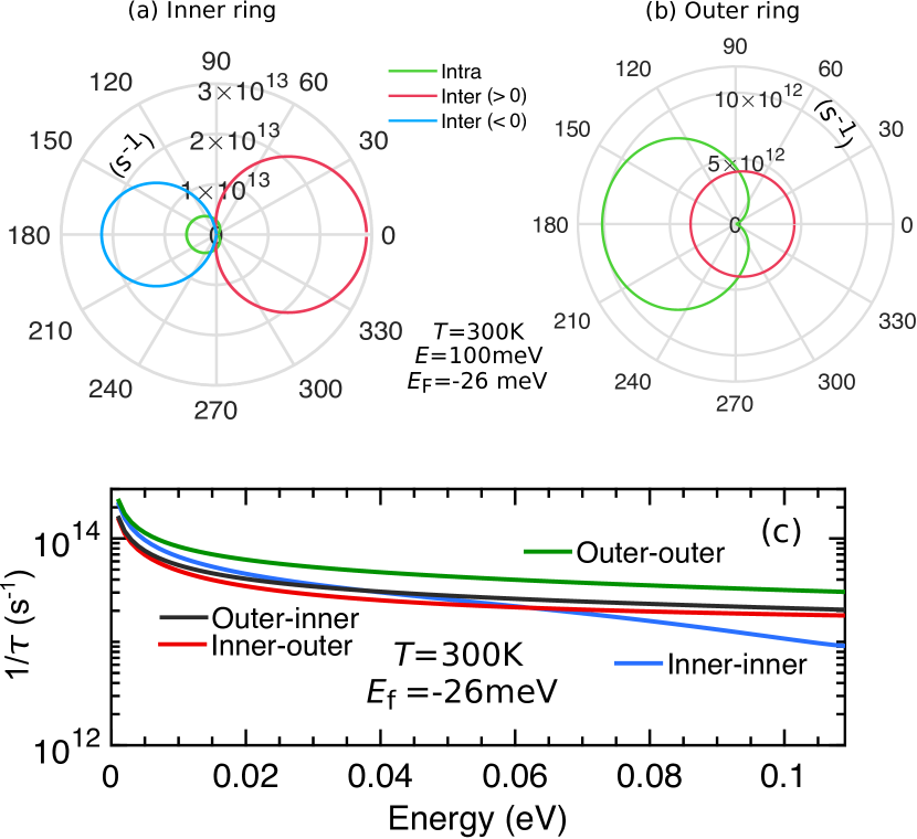
Fig. 6(c) shows the 4 components of the total scattering rate as a function of energy at K. The energy meV corresponds to the polar plots shown in (a) and (b). As the energy approaches the top of the hat, meV, the radius of the inner ring goes to zero, so that becomes independent of . The denominator in Eq. (6) is then independent of , the term integrates to zero, and the integral over gives . Thus, in the limit approaches from below, the integral in Eq. (12) can be performed analytically for both inter-ring scattering and intra-ring scattering within the inner ring. At , the single-spin density of states of both the inner ring and the outer ring are equal to . For inter-ring scattering, , and the inter-ring scattering rate is
| (16) |
where and . In the second line of Eq. (16), is the fine structure constant, is the bare electron mass, is the speed of light, is the relative mass, and is the relative dielectric constant. For intra-ring scattering within the inner ring, , and the intra-ring scattering rate becomes
| (17) |
where . The reduction of with respect to is solely the result of the increased value of as . The largest component to the total scattering rate is from scattering within the outer ring. Scattering within the outer ring allows for the largest momentum transfer and thus the smallest values of .
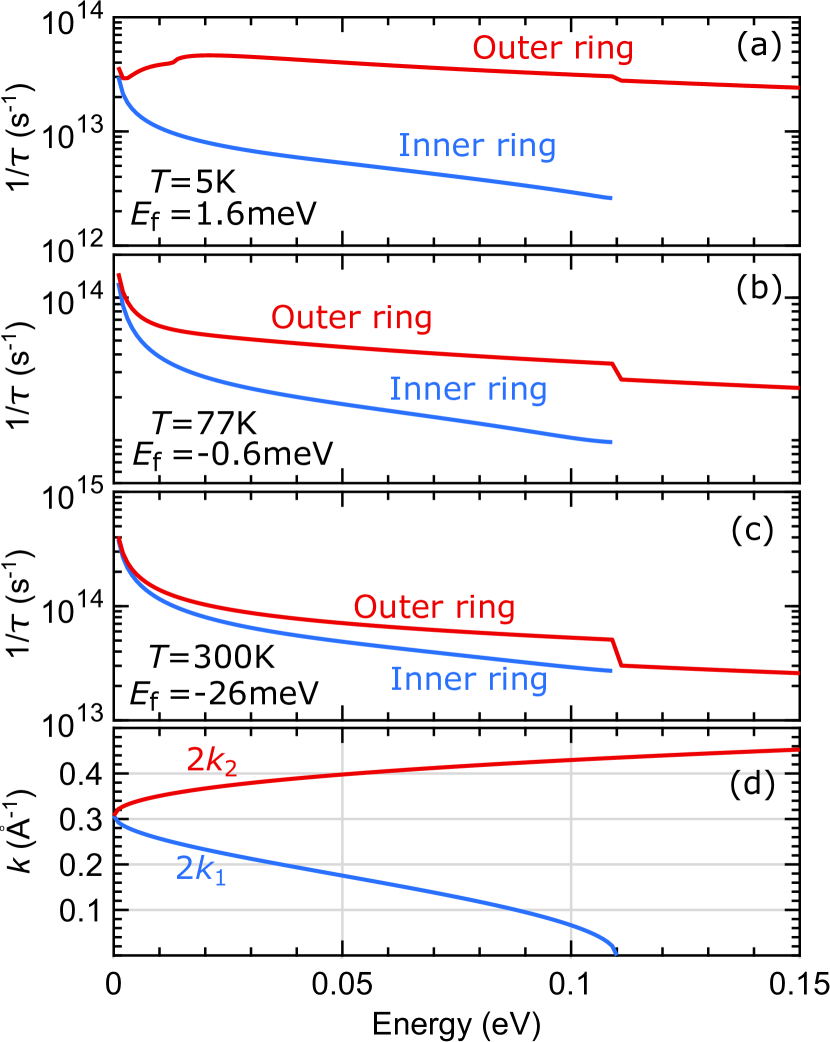
The total scattering rates for an initial state on the inner or the outer ring are shown in Fig. 7 for the same charge density () and temperatures as in Fig. 4(d). The parameters are also the same as the ones used in the calculation of the screened Coulomb matrix elements in Figs. 5 and 6. At K, as a result of the extremely large polarization, the scattering rate is suppressed for energies below 14 meV. At meV, . At energies below 14 meV, the polarization is large for all possible momentum transfer , the matrix elements of the screened Coulomb potential are reduced, and the scattering rate is reduced. The low-energy minimum occurs at meV, when the minimum inter-ring scattering momentum is where the polarization function has its maximum value. As the energy decreases below meV towards the band edge, the density of states term in Eq. (12) takes over, and the rate increases as . For momentum transfer , the polarization is negligible, and the RPA screened potential reverts to the bare unscreened potential as shown in Fig. 5(c). As the energy increases above 14 meV, unscreened backscattering takes place within the outer ring. The energy dependence for higher energies is governed by the energy dependence of the density of states and the dependence of the matrix element squared.
The radius of the inner ring is maximum at and decreases with increasing energy. Thus, the polarization relevant to the inner ring matrix elements increases with energy, causing the matrix elements to decrease. The density of states monotonically decreases and the scattering rate for states on the inner ring monotonically decreases with energy. The total rate is dominated by the intra-ring scattering of the outer ring.
At K, the polarization loses its sharp features and its magnitude is everywhere reduced causing an overall increase of the scattering rates and a monotonic decrease with energy. This trend is more pronounced at K where there is relatively little change in the sum over the range of relevant energies, and the energy dependencies of the rates are determined by the dependence of the density of states.
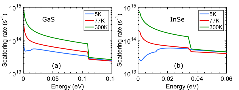
The total scattering rates for GaS and InSe are shown in Fig. 8 for temperatures of K, K and K. The temperature dependence of the overall magnitudes of the scattering rates are determined by the magnitudes of the matrix elements squared of the screened Coulomb potential, which, in turn, are determined by the temperature dependence of the polarization functions as shown in Figs. 4(d) and 5. When the energy is equal to the height of the hat, the contribution from the inner-ring scattering disappears giving an abrupt decrease in the total scattering rate at K and K. At K, the scattering rate from the inner ring is always small compared to that of the outer ring (except right at the band edge), so that the small discontinuity at is primarily the result of the disappearance of the inter-ring scattering from the outer ring to the inner ring. For energies above the top of the hat, the rates become almost identical differing by at most a factor of 1.2 for InSe. The fine differences result from the details of the different Fermi levels combined with the different thermal broadening for each different temperature. The large decrease in the K, low-energy scattering rate for InSe compared to GaS is the result of the larger polarization in InSe due to its larger mass and larger density of states.
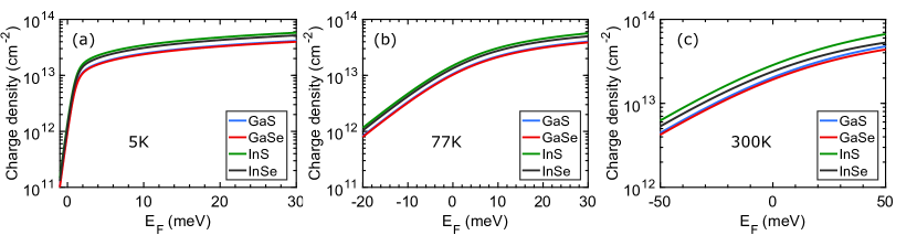
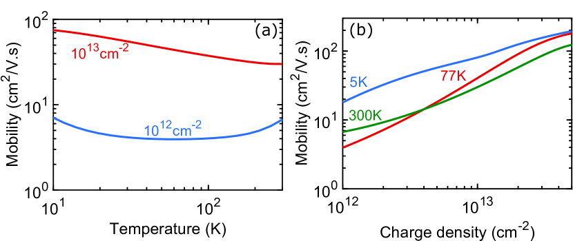
The temperature and charge density dependence of the mobility are plotted in Fig. 9. Both the temperature dependence and the density dependence of the mobility are primarily governed by the temperature and density dependence of the polarization. The initial decrease in mobility with temperature results from the decrease in polarization with temperature as shown in Fig. 4(d). The decrease in screening, increases the matrix element squared which increases the scattering rate and decreases the mobility. At K, there is a significant contribution to the integrand () of Eq. (15) from energies above . Once starts to fall inside the thermal window defined by in Eq. (15), the sudden decrease in shown in Fig. 8, gives rise to a corresponding increase in , so that the integral begins to increase with temperature. The ‘turn-on’ or ‘thermal activation’ of the mobility starts to be seen at lower temperatures for lower carrier densities as shown in Fig. 9(a). For lower carrier densities, screening is less, the matrix elements and scattering rates are larger at lower energies, the low-energy values of are reduced, and the discontinuity at is larger so that the higher energies give a disproportionally larger contribution to the mobility.
For a fixed temperature, as the charge density increases, the screening increases, which reduces the matrix element squared and the scattering rates and increases the mobility as seen in Fig. 9(b). At a charge density of cm-2, the mobility is between cm2/Vs for the 3 temperatures, 5 K, 77 K, and 300 K.
| Material | Effective mass m* (m0) | Height of the hat () (meV) | Relative permittivity |
| GaS | 0.409 | 111.2 | 3.10 |
| GaSe | 0.600 | 58.7 | 3.55 |
| InS | 0.746 | 100.6 | 3.08 |
| InSe | 0.926 | 34.9 | 3.38 |
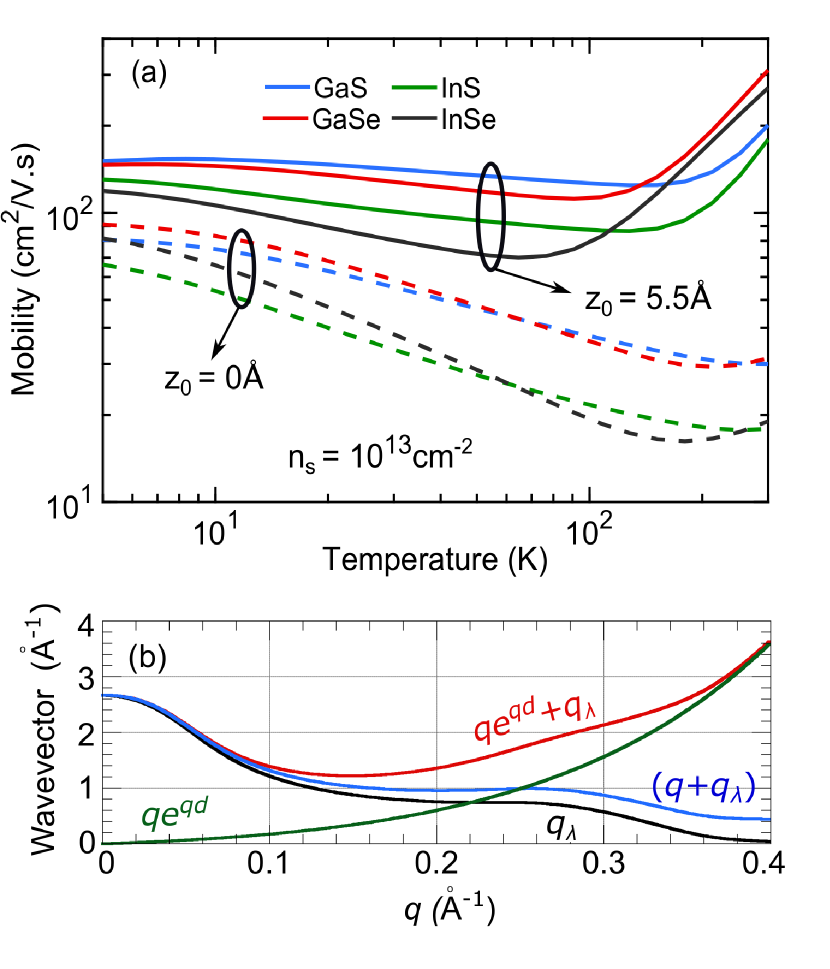
The temperature dependence of the 4 III-VI p-type materials are shown in Fig. (10) for a fixed hole density of cm-2 and two different positions of the charged impurities, in the middle of the channel (Å) and on the substrate ( Å). The relevant material parameters are given in Table 1. The general trends of the temperature dependence follow those seen in Fig. 9. The low temperature mobilities order according to the effective masses with the lower masses correlating with the higher mobilities. However, the dependence is weaker than a dependence. The minimum and maximum effective mass differ by a factor of 2.3, and at K, the mobilities differ by a factor of 1.4. The difference in mobilities increases to a maximum of 2 near the beginning of the high-temperature crossover where the mobilities start to increase. The cross-over begins at a lower temperatures for the materials with a smaller value of , since lower temperatures can thermally excite carriers above the top of the hat.
Moving the charged impurities from the middle of the channel to the substrate increases the mobility, as would be expected, since the charged impurities are further away from the carriers. However, it also lowers the temperature of the high-temperature crossover, which is not an obvious consequence. The reason lies in the large enhancement of the bare, large-wavevector screening as shown in Fig. 10(b) for GaS at K. For GaS, the bare term in the denominator becomes larger than at . The minimum value of is at the band edge, and at the top of the hat, . At that value of , the denominator is larger than at , so that backscattering across the outer ring is strongly suppressed giving a large enhancement to for energies .
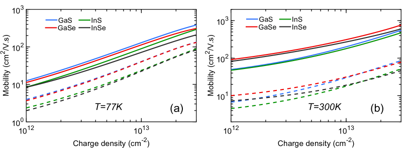
The hole density dependence of the charged impurity limited mobility at K and K is shown in Fig. (11). The mobility monotonically increases with hole density for a fixed charged impurity density . This trend would be expected due to increased screening resulting from the higher hole density. At the highest hole densities considered of cm-2, with the charged impurities on the substrate, the K mobilities lie between 500 and 800 cm2/Vs for all 4 materials. With the impurities at the center of the channel, the mobilities decrease one order of magnitude and lie in the range of 50 to 80 cm2/Vs. All mobilities are calculated for a charged impurity density of cm-2, and the mobilities are inversely proportional to , so that all mobility values shown can be easily scaled for arbitrary values of .
IV Conclusions
The Mexican hat type bandstructure that occurs in the valence band of monolayer and few layer III-VI materials and other 2D materials gives rise to unique screening properties. The singular density of states at the band edge and the two Fermi wavevectors up to the height of the hat, lead to large screening and strong wavevector dependence of the screening. The wavevector dependence of the screened Coulomb interaction is so strong, that the temperature and density dependence of the matrix element squared is the dominant factor determining the overall trends with respect to temperature and density. The reduction of polarization with temperature causes an initial increase in scattering and decrease in mobility with increasing temperature. Short wavevector inter-ring backscattering and scattering within the smaller ring is always suppressed by the large polarization at small . When the the charged impurities lie in the middle of the 2D channel, the wavevector dependence of the polarization favors large wavevector backscattering across the outer ring. When the charged impurities lie on the substrate, the bare screening increases rapidly at larger wavevectors suppressing the backscattering within the outer ring. For charged impurities on the substrate, the polarization suppresses the small wavevector scattering and the exponential wavevector dependence of the bare Coulomb interaction suppresses the large wavevector scattering across the outer ring leading to an overall increase in mobility. The suppression of the large wavevector scattering also reduces the temperature at which the mobility starts to increase when the charged impurities are on the substrate. The mobility monotonically increases with hole density up to the maximum value considered of cm-2 where it reaches a maximum value of 800 cm2/Vs for GaSe with the charged impurities located on the substrate. Placing the impurities in the center of the channel reduces the maximum value by an order of magnitude. All mobility values are calculated for a charged impurity density of cm-2 and scale inversely proportionally to .
Acknowledgements.
We acknowledge helpful discussion with Dr. Yafis Barlas. This work was supported by FAME, one of six centers of STARnet, a Semiconductor Research Corporation program sponsored by MARCO and DARPA. This work used the Extreme Science and Engineering Discovery Environment (XSEDE), which is supported by National Science Foundation Grant No. ACI-1548562 and allocation ID TG-DMR130081.References
- (1) D. Wickramaratne, F. Zahid, and R. K. Lake, Journal of Applied Physics 118, 075101 (2015).
- (2) V. Zolyomi, N. D. Drummond, and V. I. Fal’ko, Physical Review B 87, 195403 (2013).
- (3) V. Zolyomi, N. D. Drummond, and V. I. Fal’ko, Phys. Rev. B 89, 205416 (2014).
- (4) P. Hu, L. Wang, M. Yoon, J. Zhang, W. Feng, X. Wang, Z. Wen, J. C. Idrobo, Y. Miyamoto, D. B. Geohegan, and K. Xiao, Nano Letters 13, 1649 (2013).
- (5) H. L. Zhuang and R. G. Hennig, Chemistry of Materials 25, 3232 (2013).
- (6) T. Cao, Z. Li, and S. G. Louie, Phys. Rev. Lett. 114, 236602 (2015).
- (7) S. Wu, X. Dai, H. Yu, H. Fan, J. Hu, and W. Yao, arXiv preprint arXiv:1409.4733 (2014).
- (8) Y. Guo and J. Robertson, Physical Review Materials 1, 044004 (2017).
- (9) T. Stauber, N. M. R. Peres, F. Guinea, and A. H. Castro Neto, Physical Review B 75, 115425 (2007).
- (10) A. Varlet, D. Bischoff, P. Simonet, K. Watanabe, T. Taniguchi, T. Ihn, K. Ensslin, M. Mucha-Kruczyński, and V. I. Fal’ko, Phys. Rev. Lett. 113, 116602 (2014).
- (11) H. Min, B. Sahu, S. K. Banerjee, and A. H. MacDonald, Phys. Rev. B 75, 155115 (2007).
- (12) F. Zahid and R. Lake, Applied Physics Letters 97, 212102 (2010).
- (13) J. Maassen and M. Lundstrom, Applied Physics Letters 102, 093103 (2013).
- (14) Y. Saeed, N. Singh, and U. Schwingenschlögl, Applied Physics Letters 104, 033105 (2014).
- (15) Y. Li, Physical Review B 94, 245144 (2016).
- (16) L. Seixas, A. S. Rodin, A. Carvalho, and A. H. Castro Neto, Physical review letters 116, 206803 (2016).
- (17) M. Houssa, K. Iordanidou, G. Pourtois, V. V. Afanas’ ev, and A. Stesmans, ECS Transactions 80, 339 (2017).
- (18) H. Sevinçli, Nano Letters 17, 2589 (2017).
- (19) Y. Nie, M. Rahman, P. Liu, A. Sidike, Q. Xia, and G.-h. Guo, Physical Review B 96, 075401 (2017).
- (20) S. Lei, L. Ge, Z. Liu, S. Najmaei, G. Shi, G. You, J. Lou, R. Vajtai, and P. M. Ajayan, Nano Letters 13, 2777 (2013).
- (21) S. Lei, L. Ge, S. Najmaei, A. George, R. Kappera, J. Lou, M. Chhowalla, H. Yamaguchi, G. Gupta, R. Vajtai, et al., ACS nano 8, 1263 (2014).
- (22) M. Mahjouri-Samani, M. Tian, K. Wang, A. Boulesbaa, C. M. Rouleau, A. A. Puretzky, M. A. McGuire, B. R. Srijanto, K. Xiao, G. Eres, et al., Acs Nano 8, 11567 (2014).
- (23) N. Ma and D. Jena, Physical Review X 4, 011043 (2014).
- (24) Z.-Y. Ong and M. V. Fischetti, Physical Review B 88, 165316 (2013).
- (25) E. B. Kolomeisky and J. P. Straley, Physical Review B 94, 245150 (2016).
- (26) P. F. Maldague, Surface Science 73, 296 (1978).
- (27) D. A., Physica Status Solidi (b) 137, 319 (1986).