Searching for Materials with High Refractive Index and Wide Band Gap: A First-Principles High-Throughput Study
Abstract
Materials combining both a high refractive index and a wide band gap are of great interest for optoelectronic and sensor applications. However, these two properties are typically described by an inverse correlation with high refractive index appearing in small gap materials and vice-versa. Here, we conduct a first-principles high-throughput study on more than 4000 semiconductors (with a special focus on oxides). Our data confirm the general inverse trend between refractive index and band gap but interesting outliers are also identified. The data are then analyzed through a simple model involving two main descriptors: the average optical gap and the effective frequency. The former can be determined directly from the electronic structure of the compounds, but the latter cannot. This calls for further analysis in order to obtain a predictive model. Nonetheless, it turns out that the negative effect of a large band gap on the refractive index can counterbalanced in two ways: (i) by limiting the difference between the direct band gap and the average optical gap which can be realized by a narrow distribution in energy of the optical transitions and (ii) by increasing the effective frequency which can be achieved through either a high number of transitions from the top of the valence band to the bottom of the conduction or a high average probability for these transitions.
Focusing on oxides, we use our data to investigate how the chemistry influences this inverse relationship and rationalize why certain classes of materials would perform better. Our findings can be used to search for new compounds in many optical applications both in the linear and non-linear regime (waveguides, optical modulators, laser, frequency converter, etc.).
I Introduction
Light-matter interaction is at the core of various technologies (e.g. lasers, liquid-crystal displays, light-emitting diodes, …) with applications in many sectors (telecommunications, medicine, energy, transistors, microelectronics, …) Rondinelli and Kioupakis (2015). Improvement and further development of these technologies requires a thorough comprehension of the underlying physical processes and how optical properties are linked to the electronic structure. Hence, the study of the optical properties of materials has always generated considerable interest and curiosity in the scientific community (see Ref. 2 for a compilation of articles about recent developments). In particular, high refractive index materials are required to improve the performance of optoelectronic devices such as waveguide-based optical circuits, optical interference filters and mirrors, optical sensors, as well as solar cells (e.g. as anti-reflection coatings). Furthermore, according to the empirical Miller rule, high refractive index materials also potentially show high response in the non linear regime Miller (1964). In addition to having a high refractive index, the materials used in those optoelectronic devices are often required to have a wide band gap. This guarantees transparency over the visible spectral range and makes it possible for the devices to operate at higher temperatures and to switch at larger voltages Kirschman (1999). As a result, there is a strong push towards developing materials with high refractive index and wide band gap. However, while there is an abundance of systems with a wide band gap ( eV), or with a high refractive index (), there are unfortunately few materials which satisfy both requirements at the same time. The main difficulty in devising such compounds is due to the known inverse relationship between refractive index and band gap (see, e.g., Ref. 5 for a review of the different empirical or semi-empirical relations that have been proposed).
First-principles calculations have proven to be a very powerful tool to explore the electronic and optical properties of materials. Density Functional Theory (DFT) Hohenberg and Kohn (1964); Kohn and Sham (1965) provides a good description of the electronic structure, apart from a systematic underestimation of the band gap with respect to experiments. Density Functional Perturbation Theory (DFPT) Baroni et al. (1987); Gonze (1995) is widely used to predict the linear response (and related physical quantities) of periodic systems when they are submitted to an external perturbation. For instance, when considering the effect of a homogeneous electric field, DFPT allows one to compute the macroscopic dielectric function in the static limit (). The success of DFT and DFPT stems from their reliability and low computational cost. As a result, first-principles calculations have recently been combined with a high-throughput (HT) approach Hautier et al. (2012a); Curtarolo et al. (2013) targeting the discovery of new materials. Indeed, the combination of these two methods enables the creation of large databases of materials properties that would be prohibitive (in time and cost) for experimental measurements. By screening those databases, new materials, targeting specific applications, can be identified. Successful discoveries (i.e., prediction confirmed in the lab) include materials for batteries, hydrogen production and storage, thermoelectrics and photovoltaics (see, e.g., Refs. 11 and 12). Databases can also be analyzed using data mining techniques, aiming at identifying trends that can give a further insight into the comprehension of the materials properties, or even make predictions for unknown compounds through Machine Learning (see, for example, Refs. 13 and 14).
In this paper, we investigate the relationship between the refractive index and the band gap using a first-principles HT approach relying on DFT and DFPT. Our aim is to provide a statistical, “data driven”, analysis based on a large set of 4040 semiconductors. Calculated data confirm the global inverse trend between those two properties, as recently discussed in similar works Yim et al. (2015); Petousis et al. (2016, 2017). However, there is also a wide spread of the data around this general tendency, pointing out some outliers with both relatively high refractive index and wide band gap among which well-known materials (TiO2, LiNbO3, …), already widely used for optical applications, and other materials, not yet considered for such applications (Ti3PbO7, LiSi2N3, BeS, …). By mapping all the compounds onto a two-state system, a simple model is derived some descriptors of which can be accessed from the electronic structure. The density of states (DOS) at the valence and conduction band edges as well as the effective masses of those bands are found to play a critical role for achieving a high refractive index and a wide band gap simultaneously. Indeed, the availability of a large number of weakly dispersive states for optical transitions can partly counterbalance the inverse relationship between the refractive index and the band gap. Based on these considerations, we focus on the 3375 oxides present in the data set. We examine these materials in terms of their chemistry and pinpoint the most interesting ones.
II High-Throughput computation
Our database is built as follows. We start from the relaxed structures available in the Materials Project (MP) repository Jain et al. (2013). Their thermodynamical stability can be assessed by the energy above hull Ong et al. (2008); Chen et al. (2012): for a stable compound, meV/atom, and the stability decreases as increases. Here, we extract the materials with meV/atom Hautier et al. (2012b). We also include a few exceptions (with meV/atom) already investigated previously in the literature for technological applications. The 4040 selected materials cover a broad range of chemistries (oxides, fluorides, sulfides, …) with various compositions (binaries, ternaries, …). However, a significant fraction of those (3375 out of 4040) are oxides, since they show important applications in many sectors (semiconductor industry, catalysts, …) with an exceptionally broad range of electronic properties (see Ref. 22).
For all those structures, the static part of the refractive index is computed in the framework of DFPT. All the calculations are performed with the VASP software package Kresse and Furthmüller (1996), adopting the projector augmented wave (PAW) method Gajdoš et al. (2006), and using the Generalized Gradient Approximation (GGA) for the exchange-correlation functional as parameterized by Perdew, Burke, and Ernzerhoff (PBE) Perdew et al. (1996). When dealing with oxides including elements with partially occupied electrons (such as V, Cr, Mn, Fe, Co, Ni, or Mo) a Hubbard-like Coulomb term is added to the GGA (GGA+) Dudarev et al. (1998) to correct the spurious GGA self-interaction energies, adopting the values advised by the MP Jain et al. (2011). The electronic properties are calculated from the band structures available in the MP Ricci et al. (2017). For the band gap, we focus on the direct band gap, , since optical processes are related to vertical transitions. It is worth pointing out that DFT is known to underestimate the band gap up to the 50% with respect to experiments (see for example Refs. 29; 30), while a tendency to overestimate is to be expected. Further details on the validation of a similar workflow and on the error of the refractive index computed via DFPT can be found in Ref. 16.
Finally, the results (dielectric function, refractive index, space groups, etc.) are stored using the MongoDB database engine.
III Results and Discussion
III.1 Global trend
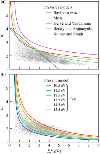
Various models have been proposed in the literature to describe the inverse relationship between the refractive index and the band gap. In Fig. 1(a), the models proposed by Ravindra et al. Ravindra et al. (1979) (green line):
Moss Moss (1985) (red line):
Hervé and Vandamme Hervé and Vandamme (1994) (cyan line):
Reddy and Anjaneyulu Reddy and Anjaneyulu (1992) (magenta line):
and Kumar and Singh Kumar and Singh (2010) (yellow line):
are superimposed on our calculated data. A detailed discussion of these models can be found in Ref. 5. It is clear that none of them follow closely the trend of the data (their mean absolute errors (MAE) range from 0.42 to 0.91) nor do they account for the wide spread of the points. It should however be mentioned that all these models were built up using a small set of experimental data points (). The model resulting from the present study is reported in Fig. 1(b). It captures the trend better than all previous models (MAE=0.33 considering eV, calculated by fitting Eq.(2) in the last square sense) and the spread in the data can be accounted for through the parameter , which will be defined below.
The inverse relationship between the refractive index and the band gap is also evident from the following equation:
| (1) | |||||
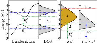
where is the polarization vector in the direction of the electric field and is the dipole matrix element for a transition from a valence state to a conduction state . Eq. (III.1) can be obtained starting from the Fermi’s golden rule Bassani and Parravicini (1975). Further details are given in the Appendix A. However, as can be anticipated from Eq. (III.1), the band gap is not a sufficient quantity to properly describe the data trend and other descriptors have to be included in the analysis. With this in mind, we map each material onto the simplest system that one can think of for describing optical transitions: a two-state (, ) system with a transition characterized by (i) an energy , (ii) a probability , and (iii) a degeneracy factor , where (resp. ) is the degeneracy of the state (resp. ). In the mapping procedure, which is schematically illustrated in the left panel of Fig. 2, is obtained as the weighted average of the transitions contributing to the optical properties (it will hence be referred to as the average optical gap). is simply the integral of , the corresponding joint density of states (JDOS), and is the average probability of those transitions. Their exact analytical expressions are given in the Appendix A. In principle, these involve integrals in an extended frequency range. In practice, one can set an upper frequency limit which is high enough compared to the optical absorption processes of interest and which can be identified by considering the optical function (see Eq. (13) of the Appendix A), as illustrated in the right panel of Fig. 2.
As a result of the mapping procedure, our data ( vs. ) shown in Fig. 1(b) can be described using the following relationship (see Eq. (21) of the Appendix A):
| (2) |
where we have further defined an effective frequency , which combines and , in order to ease the analysis.
As can be seen from Fig. 2, the average optical band gap is related to the direct band gap by:
| (3) |
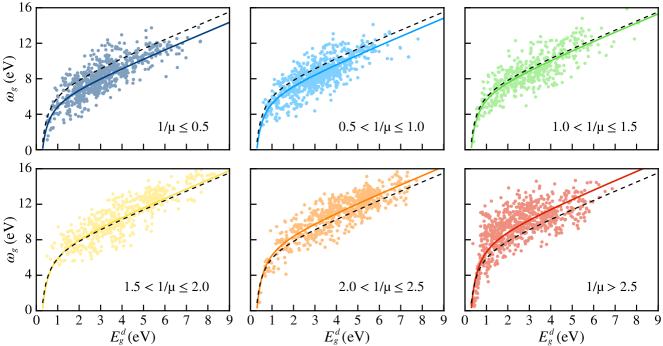
The value of is material dependent since it is influenced by the dispersion of the valence and conduction bands involved in the transition and their distribution in energy (see Fig. S3 of the Supplemental Material sup ) and, indirectly, by the direct band gap . The calculated values of and are shown in Fig. 3 for all the materials considered here.
We can describe the relationship between the quantities in Eq. (3) by the following equation (see Section I of the Supplemental Material sup for a more detailed description):
| (4) |
where =6.74 eV and =-1.19 eV2. However, we note that there is a wide spread of the data around the interpolated value (which translates into a quite large MAE of 1.20 eV for the fit).
This can be traced back to the dependence of on the width of the JDOS (see Fig. S2 of the Supplemental Material sup ) or, in other words, distribution in energy of the transitions. The simplest physical quantity that can account for this is the inverse effective mass of the transition Fox (2001) defined by
| (5) |
where and are respectively the effective mass of the valence and conduction states averaged over the three possible directions. The details of the calculation of and are given in Refs. 39; 28. By coloring the data points according to 1/ in Fig. 3, we note that the larger (the smaller the dispersion of the bands), the smaller . To improve the visualization, the full set of data has been split according to the values of . For each panel, the dashed line represents Eq. (4) with the the coefficients and reported above, and the the colored lines represent the same equation by fitting those coefficient considering each subset of data. The remaining spread in the data (other than the one coming from ) is difficult to quantify by a simple physical quantity. Part of it can probably be attributed to the distribution of the bands in energy (see Fig. S3 of the Supplemental Material sup ).
In principle, and in Eq. (4) depend on the width of the JDOS. In practice, in the rest of the paper we assume and as constants, i.e. considering the fit calculated on the overall set of data (=6.74 eV and =-1.19 eV2) to ease the discussion and the analysis.
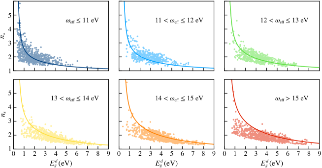
Combining Eqs. (2) and (4), we obtain a direct relationship between the average static refractive index and the direct band gap :
| (6) |
which can be compared to all the calculated data, as shown in Fig. 4. Here, the full set of data has been split according to the values of for a better visualization. In each panel, the colored lines were obtained using the same values of indicated in Fig. 1(b). Globally, the data follow the trend of Eq. (6) as represented by these lines, confirming the inverse relationship between refractive index and band gap. The agreement is quite good given the approximations that are being made for the fit of as a function of . In particular, the points with large (resp. small) effective masses can fall significantly above (resp. below) the corresponding curve (given that the latter is obtained for an average value of the effective mass).
From our analysis, it is clear that the effective frequency (combining the integral of the JDOS and the average transition probability ) and the effective mass (as well as the distribution in energy of the bands) play a key role in counterbalancing the effect of the band gap on the refractive index. The former is the numerator of the fraction appearing in Eq. (6), so the larger the higher . The latter acts on the denominator by limiting the difference between the direct band gap and the average optical gap: the larger , the smaller and hence the higher .
At this stage, we would like to emphasize that the model that we propose in Eq. (6) is not predictive. Indeed, while can be determined directly from the electronic structure of the compounds, but (and more precisely ) cannot. We leave it for another study to analyze whether machine learning might help to overcome this limitation.
III.2 Outliers
As far as the combination of high refractive index and high band gap is concerned, the most interesting materials are those lying above the curve corresponding to the value =12.10 eV, calculated by fitting in the last square sense Eq. (6) to the full set of our data. Such materials have either a large value of (i.e. following the general trend of the curves) or of (i.e. due to the spread of the data). Among those, we found various compounds commonly used for optical devices, a few examples of which are reported in Table 1. In contrast, to the best of our knowledge, some of these outliers have not yet been considered as optical materials (for instance, Ti3PbO7, LiSi2N3, BeS, …). In Section VI of the Supplemental Material sup , we provide various tables with the 10 materials with the highest refractive index for a given direct band gap range.
Having a high value of the refractive index, the compounds listed in Table 1 also show high response in the non-linear regime. In particular, LiTaO3, LiNbO3, LiB3O5, and BaB2O4 are known to have high non-linear second order coefficients. They are thus commonly used for Second Harmonic Generation (SHG), to convert the incoming light from UV, or even deep UV, to the visible spectral range (see for example Refs. 40; 41). In contrast, both TiO2 phases (anatase and rutile) are centro-symmetric and they do not show any response at the second order. But, because of their refractive index, they have been recently investigated as optical switching devices and waveguides (see for example Refs. 42; 43; 44).
| Formula | MP-id | |||||||
|---|---|---|---|---|---|---|---|---|
| LiTaO3 | mp-3666 | 2.25 | 3.71 | 14.44 | 9.05 | 3.48 | 1.44 | 1.02 |
| LiNbO3 | mp-3731 | 2.33 | 3.41 | 13.00 | 7.91 | 3.53 | 1.60 | 1.10 |
| LiB3O5 | mp-3660 | 1.62 | 6.35 | 16.13 | 13.70 | 6.77 | 1.20 | 1.02 |
| rutile-TiO2 | mp-2657 | 2.84 | 1.78 | 10.88 | 5.66 | 2.53 | 1.00 | 0.72 |
| anatase-TiO2 | mp-390 | 2.60 | 2.35 | 10.73 | 5.96 | 1.95 | 1.85 | 0.95 |
| BaB2O4 | mp-540659 | 1.63 | 4.60 | 13.46 | 11.29 | 15.01 | 0.61 | 0.58 |
III.3 Trend in oxides
We now concentrate on the 3375 oxides. We focus on the chemical composition and the electronic structure of the materials making the connection with their optical properties.
To properly describe the data distribution, we introduced the effective frequency that is related to both and (see Fig. S5 of the Supplemental Material sup ). Although both these quantities are important to obtain the correct for each material, only can be deduced from the electronic structure of the compounds. This is the main reason why our model cannot be predictive. To the best of our knowledge, there is no way to predict the probability transition just considering the band structure. Systematic correlations between and materials properties are still under investigations.
In order to analyze the trend in terms of their chemistry, the compounds are organized in four different classes: two groups of transition metal oxides (TMOs), lanthanide oxides, and main-group oxides. Materials with actinide elements are not taken in account in our analysis. These classes are created as follows: the groups of the TMOs include compounds in which there is at least one TM element with the d shell not completely filled and no lanthanide elements. The lanthanide oxides class contains compounds in which there is at least one lanthanide element, but no TM elements. Finally, the remaining oxides that do not contain any of the above mentioned elements are included in the main-group. The TMOs have been further split in two groups considering not only the TM element but also its oxidation state Waroquiers et al. (2017). In the first group, the d shell of the TM element is empty (e.g. V5+) and therefore the electronic transitions from the top of the valence to the bottom of the conduction states are expected to be from the O 2p to the TM d-orbitals. In the second group, the TM d shell is partially filled (e.g. V4+, V3+) and thus the transitions are expected to be from the TM filled d states to the empty ones. Finally, all the compounds that contain TM elements in which the d shell is completely filled (e.g. Zn2+, Cu+) are included in the main group.
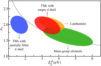
For each class, the probability density function is computed for the distribution of the refractive index as function of the band gap via a Kernel-Density Estimation (KDE) using a Gaussian kernel (see Ref. 46 for further details). The full distribution for each class of materials is reported in Fig. S6 of the Supplemental Material sup . In Fig. 5, we only represent each class by an ellipse that contains the main data distributions and is obtained as follows. Its center is located at the average value of the direct gap and refractive index for the corresponding distribution. The orientation and lengths of its axes are determined using principal component analysis for the materials which belong to the region with a density larger than 75%. The curve reported in the figure is obtained from Eq. (6) using . As we already stated, materials falling above this curve are the most interesting ones.
The importance of the flatness of the bands at the edges of the valence and conduction bands has already been underlined in Ref. 17. This means that the presence of d and f-orbitals can be helpful. Indeed, the most interesting compounds (i.e. those located mostly above this curve) come from the first group of TMOs and the lanthanide oxides, in which those orbitals are present close to the VBM and CBM. These are the most suitable for applications that require both a wide band gap and a high refractive index. This is especially true for applications for which the absorption edge is at the limit of the visible region (experimental 3 eV). For applications in the UV (experimental 6 eV), the compounds in the main group of elements reveal to be the most promising.
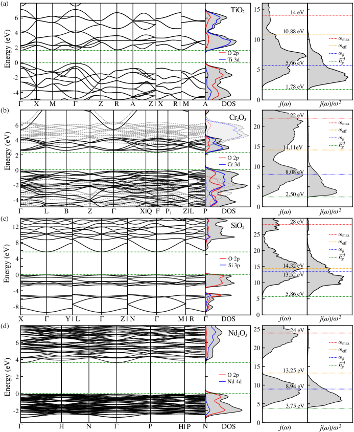
In the following subsections, we describe the peculiarities of the four different classes, focusing on a typical example for each of them. For the four representative materials, we focus on the electronic structure and on a brief description of the optical functions , and . We also highlight the different relevant quantities (, , and ).
Before proceeding with the discussion of the different classes, it is worth stressing again that the electronic structures used in this study are taken directly from the Materials Project repository. They have been obtained in the framework of DFT using the PBE exchange-correlation functional, that is known to underestimate the band gap with respect to experiments.
III.3.1 TMOs with empty d shell (1st group)
Many materials from this class are of high technological interest as dielectrics and as lenses for optical devices both in the linear and non-linear regime Cox (2010).
As can be seen in Fig. 5 (red ellipse), the materials from this class show a relatively high value for both the refractive index and the band gap. TiO2 is a typical material of this group. For this compound, the Ti oxidation state is +4 (empty d shell). This binary oxide compound still generates great interest for the construction of optical devices (see for example Refs. 47 and 48). It is indeed one of the materials with the highest value of the refractive index, while retaining a high transparency throughout the visible region. The electronic structure and the optical functions for the rutile phase (mp-2657) are shown in Fig. 6(a). These are representative of those for other known TiO2 phases (anatase, brookite, and monoclinic) and for other compounds in this class (e.g. ZrO2, V2O5, LiNbO3, …).
In all these materials, the bands at the valence and conduction edges are quite flat. The main contribution to the top valence states originates from the O 2p-orbitals, while that to the bottom conduction bands comes from the d-orbitals of the transition metal (Ti 3d in the case of TiO2). The flat nature of the bands at the edge of the band structure in this material can also be appreciated looking at the different values of the effective masses (=2.53, =1.00, =0.72). As a consequence the DOS is actually quite high at the band edges. This leads to an important originating from the transitions from the O 2p-orbitals to the transition metal d orbitals, and hence to a large value of . Further, these materials have a wide band gap that arises mainly from electron repulsion effects Zaanen et al. (1985); Harrison (2012). This translates into a high refractive index (=2.85).
In summary, for transition metals oxides from the first group, the wide band gap (which pushes the refractive index downwards) is compensated by a large number of available transitions from the top of the valence band to bottom of the conduction bands due to both the flatness of the band structure and to the high density of states at the band edges. These materials are thus very interesting candidates for further investigations.
III.3.2 TMOs with partially filled d shell (2nd group)
In general, TMOs from the second group have a smaller gap than those from the first group. This obviously pushes their refractive index upwards. However, contrary to the first group of TMOs, the majority of the data (blue ellipse in Fig. 5) fall below the curve. These materials could be considered good candidates for optical applications that require a moderate transparency (e.g. in the visible range) and a high refractive index. We focus on Cr2O3 (mp-19399) as an illustrative example with features common to other compounds of this class (e.g. PtO2, NiO…). In this case the Cr oxidation state is +3 (partially filled d shell). Chromium oxides are widely used in many sectors such as, for example, catalysis, solar energy applications, and others (further information can be found in Ref. 51). Since this material shows a magnetic ordering, in Fig. 6(b) is reported its electronic structure for both spin components separately, and the optical functions resulting from the combination of both of them. The bands at the edge of the band structure (spin up component) show a flat nature. This is further emphasized looking at the values of the effective masses (=4.29, =2.53, =1.59). At the bottom of conduction states (spin up component), as in the previous case, the main contribution comes from the d-orbitals of the TM (Cr 3d in the case of Cr2O3). One of the main difference lies in the contribution of the d-orbitals in the valence states, leading to a more hybridized character. The presence of an important amount of d states both at the top of the valence and at the bottom of the conduction leads to a decrease of the band gap with respect to the TMOs with empty d shell Zaanen et al. (1985); Harrison (2012). Due to the flatness of the bands, the DOS at the edge of the band structure is quite high giving an important . However, in this case, the JDOS gives a more broad spectrum with respect to the TiO2 case, leading to larger values of both and , and a slightly smaller value of the refractive index for Cr2O3 (=2.51).
In summary, the main difference with respect to the first group of TMOs lies in the valence bands in which there is a strong contribution from the d-orbitals. So, despite their lower gap, the TMOs from the second group show a similar refractive index.
As a final remark, it is worth to mentioning that, far this class of materials, DFT is known to predict wrong band gap and dispersion due to the presence of partially filled d-orbitals. To this purpose, as mentioned in Sec. II, a Hubbard-like Coulomb term was added (GGA+) Dudarev et al. (1998); Jain et al. (2011).
III.3.3 Main-group oxides
The main-group oxides (green ellipse in Fig. 5) show a higher diversity than the other classes. Indeed in this class we can find oxides that contain elements such as Zn, Cd and Hg in their oxidation state +2 such that they have a full d shell in valence, as well as Si, Ge, etc. Although the compounds in this class show a common behavior in terms of their electronic structure, due to the diversity of the materials their band gaps display a more important spread.
Most of the materials belonging to this class are commonly used as insulators. A prototypical example of this class SiO2. This material is used for many devices and one of the most known applications is found in the amorphous silica phase, used for optical fibers Senior (2009). The electronic structure and the optical functions for the -cristobalite tetragonal form (mp-546794) are shown in Fig 6(d). Here, as in the case of the first group of transition metals oxides, O 2p states lead to quite flat valence bands and increase the DOS at the valence edge. In contrast, the conduction bands are very dispersive, showing almost a free-electron like parabolic character which directly translates into the values of the effective masses (=4.15, =0.56, =0.49). This results in a small contribution to the DOS at the bottom of the conduction states. Consequently, the JDOS [Fig. 6(c)] does not show any clear peak close to the absorption edge and the refractive index is quite low (=1.48). Indeed the value of for this material is smaller than the one of both the representative candidates previously described. Furthermore, compared to the other cases, the value of is much higher than that of (), and it is much closer to .
III.3.4 Lanthanide oxides
Lanthanide oxides (orange ellipse in Fig. 5) tend to have a wide band gap, while still showing a high refractive index. The oxides contained in this class have common features with the TMOs with empty d shell. Indeed, the two respective ellipses are almost superimposed on each other in Fig. 5. As an illustrative example, we have chosen Nd2O3 (mp-1045). These compounds are typically known because they show good luminescence properties and they can be used as fluorescent materials in lighting applications (more information can be found in Ref. 53). Looking at the electronic structure, the flat nature of the bands can be appreciated at the top of the valence states coming mainly from the O 2p-orbitals. At the bottom of the conduction states, there is a slightly more dispersive behavior that comes mainly from the d-orbitals (Nd 4d in the case of Nd2O3). This is also evident looking at the values of the effective mass (=6.81, =0.53, =0.50). As a result, the DOS at the top of the valence is quite important (as in the case of the 1st group of TMOs), but the slightly more dispersive nature of the bands at the bottom of the conduction leads to a less pronounced DOS. Anyway, shows a pretty well-defined peak centered at around . The large availability of states for an electronic transition from valence to conduction turns into a large value of , leading to reasonably high value of the refractive index (=2.06). All these considerations show the similarity between this class of oxides and the 1st group of TMOs, and explain why the refractive index remains high in despite the wide band gap.
Finally, we would like to emphasize that the results for the lanthanide oxides need to be taken with great caution. Indeed, it is not a simple task to accurately compute materials with f electrons from first principles relying on pseudopotentials. In many cases, these electrons are frozen in the core, which may lead to a lack of accuracy.
IV Conclusions
In this study, we have performed a high-throughput investigation of the electronic and optical properties of 4040 semiconductors, calculating their band gap and static refractive index in the framework of density functional theory and density functional perturbation theory. Our data confirm the inverse relationship between and , but outliers are identified that combine a wide band gap with a high refractive index. Some of these are well-known optical materials (e.g. TiO2, LiNbO3, …) while others have never been considered in this framework to the best of our knowledge (e.g. Ti3PbO7, LiSi2N3, BeS, …).
By mapping all the compounds onto a two-state system, two main descriptors are identified: the average optical gap and the effective frequency. While the former can be deduced directly from the electronic structure, the latter cannot. This limits the predictive power of our model and calls for further analysis (e.g. using a machine-learning approach). However, the model highlights that the decrease of with can be partly counterbalanced by a high number and density of available transitions from the top of the valence band to the bottom of the conduction band. This is directly related to the density of states at the edges of those bands and to the effective mass of such states.
By considering the compounds based on their chemical composition, we have then extracted some common features that can be useful in achieving a wide band gap dielectric. We have found that materials belonging to the first class of transition metal oxides and lanthanide oxides are the most promising ones for optical applications that require a wide band gap and a high refractive index.
Though our data were collected for materials in the linear regime, they can also be used as a starting point for an analysis of optical properties in the nonlinear regime. It is worth stressing that our main conclusions are inferred merely from a statistical approach. Such an approach can help in the understanding and construction of optical devices in a wide range of applications.
Acknowledgments
The authors acknowledge X. Gonze and A. Tkatchenko for useful discussions. FN was funded by the European Union’s Horizon 2020 research and innovation programme under the Marie Sklodowska-Curie grant agreement N∘ 641640 (EJD-FunMat). GMR is grateful to the F.R.S.-FNRS for financial support. GH, GMR and FR acknowledge the F.R.S.-FNRS project HTBaSE (contract N∘ PDR-T.1071.15) for financial support. We acknowledge access to various computational resources: the Tier-1 supercomputer of the Fédération Wallonie-Bruxelles funded by the Walloon Region (grant agreement N∘ 1117545), and all the facilities provided by the Université catholique de Louvain (CISM/UCL) and by the Consortium des Équipements de Calcul Intensif en Fédération Wallonie Bruxelles (CÉCI).
Appendix A Theory
In the linear regime, the dielectric function of a material is the coefficient of proportionality between the macroscopic displacement field and the macroscopic electric field . In the most general form, both fields are frequency-dependent and they are not necessarily aligned (e.g. in an anisotropic material). The dielectric function is thus a frequency-dependent tensor (where ,=1,,3 span the space directions):
| (7) |
For sake of simplicity, we will avoid the tensor notation and refer to it simply as . In general, the displacement field will include contributions from both electronic and ionic displacements; but in the optical regime, the former dominates. This optical (ion-clamped) dielectric permittivity tensor is the one of interest for the present paper.
The refractive index is related to the dielectric function by:
| (8) |
where and are the real and imaginary parts of , respectively. In the static limit (), the imaginary part of the dielectric function vanishes for semiconductors, and Eq. (8) becomes:
| (9) |
In quantum mechanics, the dielectric function can be related to band-to-band transitions. Its imaginary part can be obtained from Fermi’s golden rule as:
| (10) |
where is the polarization vector in the direction of the electric field and are the dipole matrix elements for a transition from a valence state to a conduction state . The sum goes over all valence and, in principle, conduction states. In practice, a convergence test is performed with respect to the number of conduction states to be included in the sum.
The real part of the dielectric function can be derived from its imaginary part via the Kramers-Kronig relations:
| (11) |
where P indicates the principal part of the integral. In the static limit, it gives:
| (12) |
In principle, the above integral has to be taken from zero to infinity. In practice, a typical spectrum usually reveals well-separated peak regions, with little overlap, due to different absorption processes. Therefore, one can set an upper frequency limit which is high enough compared to the optical absorption processes of interest here, but small compared to other ones. In this work, is defined in such a way that:
| (13) |
The value of and hence can be directly calculated using DFPT at low computational cost Baroni and Resta (1986); Baroni et al. (1987); Giannozzi et al. (1991); Gonze (1997); Gonze and Lee (1997). Indeed, conduction states do not need to be taken into account in contrast with the sum over states formulation within the random-phase approximation Adler (1962); Wiser (1963). The drawback of the DFPT approach is that only the static limit of the dielectric function is computed and hence the frequency dependence is not available. This can be partly circumvented as follows.
We first introduce the joint density of states (JDOS):
| (14) |
which can easily be obtained from DFT calculations of the electronic band structure. We note its similarity with Eq. (A). As a result, we define a frequency-dependent transition probability such that:
| (15) |
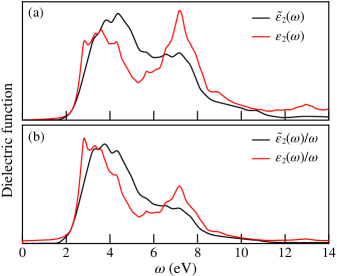
We note that, if the matrix elements were all equal to a constant , we would simply have . In Fig. A1, we show, as an example, a comparison between the frequency-dependent transition probability and the constant value for a real material.
Consequently, a simple approximation for the imaginary part of the dielectric function can be obtained as Bassani and Parravicini (1975):
| (16) |
The value of is determined such that also satisfies the Kramers-Kronig relation given by Eq. (12). This is strictly equivalent to defining as a weighted average of as follows:
| (17) |
A comparison of with is given in Fig. A2.
Using this approximation for the imaginary part of the dielectric function, Eq. (12) can be rewritten as follows:
| (18) |
Introducing the integral of the JDOS , we further define the effective frequency :
| (19) |
and the average optical gap :
| (20) |
Finally, we can thus write:
| (21) |
which is Eq. (2) in the main text.
References
- Rondinelli and Kioupakis (2015) J. M. Rondinelli and E. Kioupakis, Annu. Rev. Mater. Res. 45, 491 (2015).
- Odom et al. (2015) T. W. Odom, R. M. Dickson, M. A. Duncan, and W. Tan, ACS Photonics 2, 787 (2015).
- Miller (1964) R. C. Miller, Appl. Phys. Lett. 5, 17 (1964).
- Kirschman (1999) R. K. Kirschman, High temperature electronics (New York : IEEE Press, 1999).
- Tripathy (2015) S. Tripathy, Opt. Mater. 46, 240 (2015).
- Hohenberg and Kohn (1964) P. Hohenberg and W. Kohn, Phys. Rev. 136, B864 (1964).
- Kohn and Sham (1965) W. Kohn and L. J. Sham, Phys. Rev. 140, A1133 (1965).
- Baroni et al. (1987) S. Baroni, P. Giannozzi, and A. Testa, Phys. Rev. Lett. 58, 1861 (1987).
- Gonze (1995) X. Gonze, Phys. Rev. A 52, 1086 (1995).
- Hautier et al. (2012a) G. Hautier, A. Jain, and S. P. Ong, J. Mater. Sci. 47, 7317 (2012a).
- Curtarolo et al. (2013) S. Curtarolo, G. L. W. Hart, M. B. Nardelli, N. Mingo, S. Sanvito, and O. Levy, Nat. Mater. 12, 191 (2013).
- Jain et al. (2016) A. Jain, Y. Shin, and K. A. Persson, Nat. Rev. Mater. 1, 15004 (2016).
- Morgan et al. (2004) D. Morgan, G. Ceder, and S. Curtarolo, Meas. Sci. Technol. 16, 296 (2004).
- Hansen et al. (2013) K. Hansen, G. Montavon, F. Biegler, S. Fazli, M. Rupp, M. Scheffler, O. A. von Lilienfeld, A. Tkatchenko, and K.-R. Müller, J. Chem. Theory Comput. 9, 3404 (2013).
- Yim et al. (2015) K. Yim, Y. Yong, J. Lee, K. Lee, H.-H. Nahm, J. Yoo, C. Lee, C. Seong Hwang, and S. Han, NPG Asia Mater. 7, e190 (2015).
- Petousis et al. (2016) I. Petousis, W. Chen, G. Hautier, T. Graf, T. D. Schladt, K. A. Persson, and F. B. Prinz, Phys. Rev. B 93, 115151 (2016).
- Petousis et al. (2017) I. Petousis, D. Mrdjenovich, E. Ballouz, M. Liu, D. Winston, W. Chen, T. Graf, T. D. Schladt, K. A. Persson, and F. B. Prinz, Sci. Data 4, 160134 (2017).
- Jain et al. (2013) A. Jain, S. P. Ong, G. Hautier, W. Chen, W. D. Richards, S. Dacek, S. Cholia, D. Gunter, D. Skinner, G. Ceder, and K. A. Persson, APL Mater. 1, 011002 (2013).
- Ong et al. (2008) S. P. Ong, W. Lei, B. Kang, and G. Ceder, Chem. Mater. 20, 1798 (2008).
- Chen et al. (2012) H. Chen, G. Hautier, A. Jain, C. Moore, K. Byoungwoo, R. Doe, L. Wu, Y. Zhu, Y. Tang, and G. Ceder, Chem. Mater. 24, 2009 (2012).
- Hautier et al. (2012b) G. Hautier, S. P. Ong, A. Jain, C. J. Moore, and G. Ceder, Phys. Rev. B 85, 155208 (2012b).
- Cox (2010) P. A. Cox, Transition Metal Oxides: An Introduction to Their Electronic Structure and Properties (Oxford, 2010).
- Kresse and Furthmüller (1996) G. Kresse and J. Furthmüller, Comput. Mater. Sci. 6, 15 (1996).
- Gajdoš et al. (2006) M. Gajdoš, K. Hummer, G. Kresse, J. Furthmüller, and F. Bechstedt, Phys. Rev. B 73, 045112 (2006).
- Perdew et al. (1996) J. P. Perdew, K. Burke, and M. Ernzerhof, Phys. Rev. Lett. 77, 3865 (1996).
- Dudarev et al. (1998) S. L. Dudarev, G. A. Botton, S. Y. Savrasov, C. J. Humphreys, and A. P. Sutton, Phys. Rev. B 57, 1505 (1998).
- Jain et al. (2011) A. Jain, G. Hautier, S. P. Ong, C. J. Moore, C. C. Fischer, K. A. Persson, and G. Ceder, Phys. Rev. B 84, 045115 (2011).
- Ricci et al. (2017) F. Ricci, W. Chen, U. Aydemir, G. J. Snyder, G.-M. Rignanese, A. Jain, and G. Hautier, Sci. Data 4, 170085 (2017).
- Agapito et al. (2015) L. A. Agapito, S. Curtarolo, and M. Buongiorno Nardelli, Phys. Rev. X 5, 011006 (2015).
- Chan and Ceder (2010) M. K. Y. Chan and G. Ceder, Phys. Rev. Lett. 105, 196403 (2010).
- Ravindra et al. (1979) N. M. Ravindra, S. Auluck, and V. K. Srivastava, Phys. Status Solidi B 93, K155 (1979).
- Moss (1985) T. S. Moss, Phys. Status Solidi B 131, 415 (1985).
- Hervé and Vandamme (1994) P. Hervé and L. Vandamme, Infrared Phys. Technol. 35, 609 (1994).
- Reddy and Anjaneyulu (1992) R. R. Reddy and S. Anjaneyulu, Phys. Status Solidi B 174, K91 (1992).
- Kumar and Singh (2010) V. Kumar and J. Singh, Indian J. Pure Appl. Phys. 48, 571 (2010).
- Bassani and Parravicini (1975) G. F. Bassani and G. P. Parravicini, Electronic states and optical transitions in solids (Pergamon Press, 1975).
- (37) See Supplemental Material at [URL will be inserted by publisher].
- Fox (2001) A. Fox, Optical Properties of Solids, Oxford master series in condensed matter physics (Oxford University Press, 2001).
- Hautier et al. (2014) G. Hautier, A. Miglio, D. Waroquiers, G.-M. Rignanese, and X. Gonze, Chem. Mater. 26, 5447 (2014).
- Boyd (2008) R. W. Boyd, Nonlinear Optics, Third Edition, 3rd ed. (Academic Press, Inc., Orlando, FL, USA, 2008).
- Tran et al. (2016) T. T. Tran, H. Yu, J. M. Rondinelli, K. R. Poeppelmeier, and P. S. Halasyamani, Chem. Mater. 28, 5238 (2016).
- Evans et al. (2012) C. C. Evans, J. D. B. Bradley, E. A. Martí-Panameño, and E. Mazur, Opt. Express 20, 3118 (2012).
- Evans et al. (2013) C. C. Evans, K. Shtyrkova, J. D. B. Bradley, O. Reshef, E. Ippen, and E. Mazur, Opt. Express 21, 18582 (2013).
- Evans et al. (2015a) C. C. Evans, K. Shtyrkova, O. Reshef, M. Moebius, J. D. B. Bradley, S. Griesse-Nascimento, E. Ippen, and E. Mazur, Opt. Express 23, 7832 (2015a).
- Waroquiers et al. (2017) D. Waroquiers, X. Gonze, G.-M. Rignanese, C. Welker-Nieuwoudt, F. Rosowski, M. Göbel, S. Schenk, P. Degelmann, R. André, R. Glaum, and G. Hautier, Chem. Mater. 29, 8346 (2017).
- Scott (1979) D. W. Scott, Biometrika 66, 605 (1979).
- Evans et al. (2015b) C. C. Evans, C. Liu, and J. Suntivich, Opt. Express 23, 11160 (2015b).
- Evans et al. (2016) C. C. Evans, C. Liu, and J. Suntivich, ACS Photonics 3, 1662 (2016).
- Zaanen et al. (1985) J. Zaanen, G. A. Sawatzky, and J. W. Allen, Phys. Rev. Lett. 55, 418 (1985).
- Harrison (2012) W. A. Harrison, Electronic structure and the properties of solids: the physics of the chemical bond (Courier Corporation, 2012).
- Abdullah et al. (2014) M. M. Abdullah, F. M. Rajab, and S. M. Al-Abbas, AIP Advances 4, 027121 (2014).
- Senior (2009) J. M. Senior, Optical Fiber Communications Principles and Practice (Pearson Education, 2009).
- Bazzi et al. (2005) R. Bazzi, A. Brenier, P. Perriat, and O. Tillement, J. Lumin. 113, 161 (2005).
- Baroni and Resta (1986) S. Baroni and R. Resta, Phys. Rev. B 33, 7017 (1986).
- Giannozzi et al. (1991) P. Giannozzi, S. de Gironcoli, P. Pavone, and S. Baroni, Phys. Rev. B 43, 7231 (1991).
- Gonze (1997) X. Gonze, Phys. Rev. B 55, 10337 (1997).
- Gonze and Lee (1997) X. Gonze and C. Lee, Phys. Rev. B 55, 10355 (1997).
- Adler (1962) S. L. Adler, Phys. Rev. 126, 413 (1962).
- Wiser (1963) N. Wiser, Phys. Rev. 129, 62 (1963).