Magnetoelectronics; spintronics: devices exploiting spin polarized transport or integrated magnetic fields Spin polarized transport Reprogrammable magnetic logic
Simultaneous spin-based Boolean logic operations with re-programmable functionality
Abstract
Construction of parallel logic gates at nano-scale level undoubtedly improves the efficiency of computable operations. In this work we put forward a new idea of designing two distinct logical operations simultaneously in the two output leads of a three-terminal bridge setup which on one hand is highly stable as all the results are valid for a wide range of parameter values and on the other hand easy to engineer. Our system can be reprogrammed to have all the two-input logic gates with two operations at a time by selectively choosing the physical parameters describing the system, viz, Rashba spin-orbit (SO) interaction, magnetic flux, and Fermi energy. Finally, we explore the possible storage mechanism as well using our model.
pacs:
85.75.-dpacs:
72.25.-bpacs:
85.75.Ff1 Introduction
The logic gates are the most essential bricks of modern computers and digital electronics as their functionalities rely on the implementation of Boolean functions. These gates are usually comprised of various field-effect transistors (FETs) and metal oxide semiconductor field effect transistors (MOSFETs). So, finding of logical responses in a simple nano-scale device is a subject of intense research for better performance of computable operations. And for proper execution of such operations, wiring between individual logic gates is definitely required which limits integration densities, gives rise to huge power consumption and restricts processing speeds [1]. Therefore, accommodation of Boolean logic gates into a single active element is highly desirable to eliminate wiring amongst transistors.
Though a wealth of literature knowledge has been developed in designing logic gates essentially based on molecular systems [2, 3, 4], but most of these works are involved in single logic operation at a time, and very less number of works are available so far in the context of functioning parallel logic gates in one setup which is highly desirable from the efficiency perspective and suitable computable operations. Hod et al. [5] have made an effort to design parallel logic gates considering a cyclic molecule where a realistic magnetic field and gate potential are used as the inputs. In their work they have only shown AND and NAND operations. A completely different prescription was given by imposing a novel architecture considering a single parametric resonator (electromechanical) where three logical operations along with multibit logic functions can be performed [1]. This work essentially suggests a suitable prospect of designing parallel logic processor using a single resonator. There are other few realizations of parallel logic operations [6, 7, 8, 9] considering different semi-conducting materials, molecular systems, protein-like molecules, synthetic gene networks. But these studies do not essentially address the phenomenon of ‘simultaneous Boolean logical operations’, which is precisely our main motivation of the present work.
Most of the works available in literature exploit electronic charge for logical operations, but the implementation of these functional operations based on spin degree of freedom undoubtedly yields several advantages like rapid processing, much smaller energy consumptions, greater integration densities, etc. [10, 11]. In order to design an efficient spintronic device be it logic functions or any other operations, we need to take care about two important things: spin injection efficiency and spin coherence length. Metallic systems are much superior than semiconducting materials in the aspect of spin injection, but the previous ones have much lower spin coherence length [12]. Both these two facts viz, efficient spin injection and coherence length, can be incorporated if we can construct the device using normal metal by compromising on system size. Hopefully it can be done with suitable designing of the setup, and we explore it in this article. Here we also circumvent the consideration of molecular systems, as normally used in describing logic operations, due to the fact that they exhibit much lower transconductance [13].
Considering all these factors, here we propose a new idea of designing ‘simultaneous Boolean logic operations’ using a three-terminal bridge setup (see Fig. 1) where the output response is fully spin based. In the two outgoing leads we get two different logical operations at an
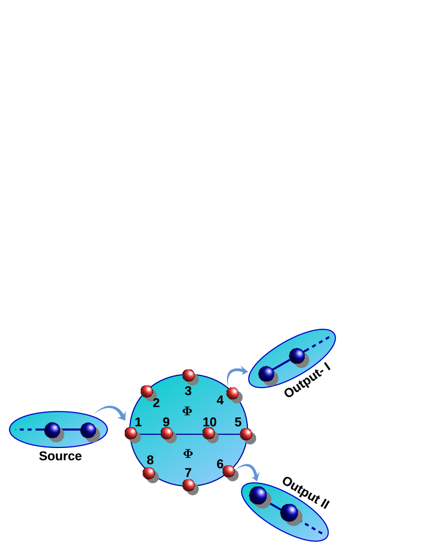
identical time which we measure by calculating spin current , and the central mechanism is controlled by the system placed within the three contacting leads. The bridging system consists of a metallic ring which is divided equally to form two sub-rings. Apart from the common portion of the two sub-rings (viz, the dividing line connecting the sites , , and ), the rest section (i.e., the ring circumference joining the sites , , , and ) is subjected to Dresselhaus SO interaction (DSOI) [14], and it is distributed uniformly throughout the ring. Along with this we also consider Rashba SO interaction (RSOI) [15] where two different cases, viz, uniform and non-uniform, are considered for the distribution of RSOI along the ring circumference to implement specific simultaneous logic operations, and it will be clearly observed from our subsequent analysis. Both these two SO interactions are commonly encountered in solid state materials and among them RSOI draws much attention as its strength can be tuned externally [16, 17] which yields controlled spin transmission. We use RSOI as one of the input signals of logic operations, and, in some cases we also introduce equal amount of magnetic flux in the two sub-rings which is treated as another input signal. The ‘ON’ and ‘OFF’ states of the output signal are described by the positive and negative signs of , respectively, where ( being the spin dependent current). By selectively choosing the physical parameters, viz, RSOI, magnetic flux and Fermi energy, the present setup can be ‘reprogrammed’ to have all the six two-input Boolean logic gates with two operations at a time. Achieving these parallel logic operations we can also think about other special-purpose logic operations [18] like full-adder, half-adder, multiplier, switching spin action, etc.
The rest of the paper is arranged as follows. With the above brief introduction and motivation, next we illustrate our model quantum system and the theoretical prescription for the calculations. The logical operations are clearly described in a separate section. In this section we also discuss the possibilities of utilizing the setup for storage mechanism. Logical operations along with storage function is extremely important for the complete executation of computable operation and that is hopefully possible as our response is spin based. In usual charge based devices we need to transfer the information to a memory as these are usually highly volatile [18]. Finally, we end with conclusion and future perspectives of spintronic applications.
2 Model Hamiltonian and the Method
The full bridge system described in Fig. 1 is divided into three parts: the central ring conductor, three leads (one incoming and two outgoing), and conductor-to-lead coupling. We simulate these parts by the tight-binding (TB) framework. Assuming the leads are perfect and semi-infinite, we can write the TB Hamiltonian of the leads as
| (1) |
where the summation over ( runs from to ) is used for the three leads. The parameters and describe the on-site energy and nearest-neighbor hopping (NNH) integral, respectively. For an ordered lead we can easily put , without loss of any generality. controls the band width () of the leads. We couple the incoming lead at site of the ring, for the entire analysis, whereas the other two leads are connected at two other sites of the ring (say, and ), those are variables. The leads are coupled to the ring through the hopping parameter .
The TB Hamiltonian for the central system looks quite different from Eq. 1, as the ring system is subjected to Rashba and Dresselhaus SO interactions, and the magnetic flux as well. The dividing line is free from any kind of SO interaction, and since the two sub-rings are threaded by equal amount of magnetic flux, no phase factor will introduce into this segment. We write the general Hamiltonian of the central ring (CR) geometry as [19, 20, 21, 22]
| (2) | |||||
where is a column of operators formed with the fermionic operators and . is the phase factor acquired by an electron [23] while traversing through the periphery of the ring. In this Hamiltonian we do not consider any spin splitting mechanism due to Zeeman interaction, as it is too small compared to the other two splitting mechanisms associated with the Rashba and Dresselhaus SO couplings. With this assumption no physical picture will be altered. The Rashba and Dresselhaus SO interactions are described by the factors and , respectively, and ( being the total number of atomic sites in the ring, and for our schematic diagram it is ) which defines the factor . The other physical parameters and represent on-site energy and NNH integral in the ring as well as in the central wire. ’s () are the usual Pauli spin matrices where is diagonal.
This is all about the model and the TB Hamiltonians describing the full system. Now, in order to describe the logical responses in two outgoing leads we need to calculate spin currents. At absolute zero temperature, the spin current at th lead ( can be lead-2 (i.e., output-I) and lead-3 (i.e., output-II)) is computed from the relation [24]
| (3) |
where is the effective two-terminal spin selective transmission probability, and it is defined as . To find spin dependent transmission probabilities we use Green’s function method, and in terms of the retarded and advanced Green’s functions (, ) it can be expressed as [24, 25, 26] , where are the coupling matrices and . is the effective Hamiltonian of the central ring system by incorporating the effects of side-attached leads through self-energy corrections. In our prescription, positive means high output, while negative corresponds to the low output.
3 Essential Results and Discussion
Simultaneous logical operations: As already stated above, by selectively choosing physical parameters, viz, Rashba SO coupling, magnetic flux in each sub-rings and location of the outgoing leads we can design all possible Boolean logic gates, two such gates at a time. Here we present three pairs (OR-NOR, AND-NAND, and XOR-XNOR) for a specific set of parameter values, as illustrative examples, but one can get other different pairs quite easily simply by adjusting the required variables, and thus, our system is reprogrammable.
We carry out numerical calculations at absolute zero temperature, considering a -site system as discussed in Fig. 1. Throughout the analysis we set, unless otherwise specified, all site energies to zero, NNH integral in contacting leads at eV, and the rest other NNH integrals including ring-to-lead coupling at eV. The DSOI is fixed at eV, and it is uniform throughout the ring circumference as stated earlier. The other two physical parameters, RSOI and , are no longer constant and we mention their specific values during the subsequent analysis. In what follows we present different functional logical operations one by one.
Case I. OR and NOR operations: The setup is shown in Fig. 2(a) where the outgoing leads are coupled to sites and , respectively, of the ring. Here two different strengths of RSOI are taken into account those are treated as low and high states of the inputs, and no magnetic
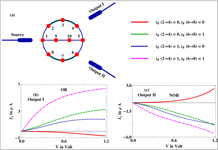
flux is added. These two input states are implemented by changing the Rashba strengths at the green portions of the upper and lower arms of the ring (see Fig. 2(a)), keeping a constant magnitude of RSOI in the other parts. It looks like a hybrid ring and seems quite easy to fabricate. The responses for this setup at the two outgoing leads under different input conditions are shown in Figs. 2(b) and (c). The spin current is computed up to a reasonable bias voltage, and for this entire voltage window we can clearly see that the two outgoing leads exhibit two different logical operations (OR and NOR) simultaneously. The output currents are also sufficiently high (A) which thus easy to detect. The underlying physics involved relies on the interplay between RSOI and DSOI which leads to anisotropic spin dependent transport in the outgoing leads as discussed clearly by Chang and co-workers [19, 27, 28]. In presence of both the two SO couplings, an effective periodic potential is developed which breaks the rotational symmetry of the ring, resulting non-trivial spin dependent transport phenomena [19, 27, 28]. To achieve simultaneous logical operations we essentially need to get polarized spin currents from an unpolarized beam of electrons in outgoing leads of a multi-terminal bridge setup. Several propositions have already been made by some groups and by one of the authors of us along this direction
i.e., how to get polarized spin currents in presence of SO interactions in outgoing leads considering different shaped geometries [29, 30, 31, 32, 33]. The main focus of those works was to achieve polarized spin currents under different input conditions, but no one has attempted to think about logical operations, especially simultaneous logic functions. This is precisely what we do in our present work, and the responses what we get in two outgoing leads are basically the combined effect of SO interactions and quantum interference of electronic waves passing through different sectors of the geometry. Here it is important to note that all the logical operations are implemented by determining the spin current , and more precisely by noting its sign viz, positive or negative. Thus, for two logical operations at the two output leads, we need to satisfy all the operations simultaneously (a set of four outputs for each logic gates) associated with the input conditions, and we achieve this goal considering the interplay between the RSOI and DSOI, and the interference among the electronic waves. If we set any one the two SO interactions to zero, which brings back the rotational symmetry in the ring [29, 30, 31, 32], it will be too hard to satisfy all the above mentioned operations at the two output leads. Particularly, when DSOI becomes zero (for instance), no spin current will be available for the input condition where RSOI is also zero, which thus fails to explain logic functions. In that case we have to consider non-zero Rashba couplings for the inputs, but satisfying all the output conditions will not be quite simple unlike the cases we discuss here with our present setups.
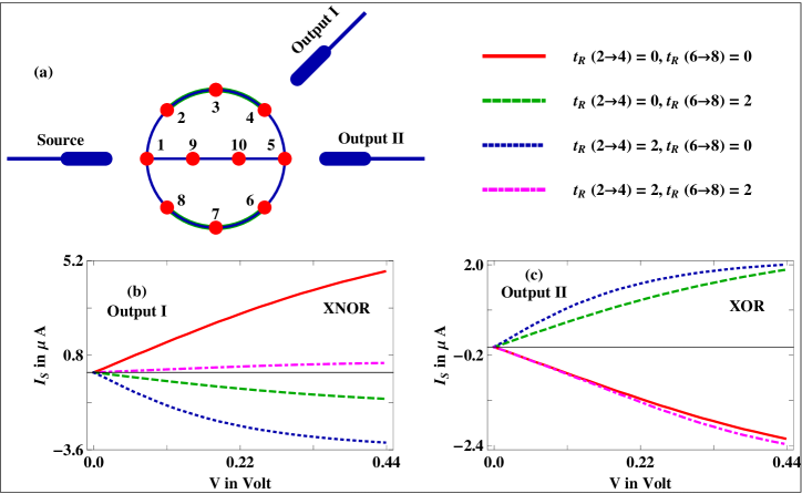
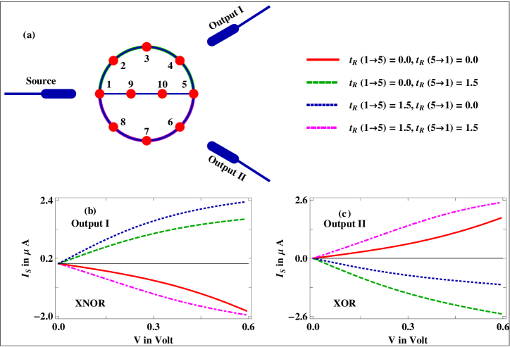
Case II. XOR and XNOR operations: Considering the identical ring type (viz, the hybrid ring where RSOI is distributed non-uniformly) as taken in Case I, and slightly modifying the location of one of the two outgoing
leads we get a pair of another two simultaneous logical operations. The setup along with the results are placed in Fig. 3, where we see that XOR and XNOR operations are clearly obtained from the two outgoing leads. We simulate these results setting the equilibrium Fermi energy at eV. Comparing the results given in Figs. 2 and 3 we get a clear hint about the robust effect of quantum interference as in one case a specific set of two logical operations are obtained, while another such set is visible for the other case.
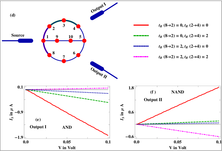
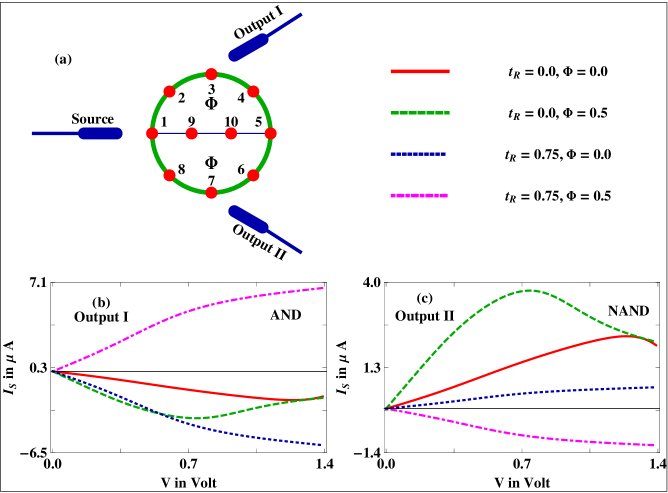
Case III. AND and NAND operations: Finally, we consider another configuration to implement other two logic functions i.e., AND and NAND operations. Here the full circumference is subjected to Rashba SO interaction which acts as one of the two input signals, and for the other input we impose equal amount of magnetic flux in each of the two sub-rings as shown schematically in Fig. 4(a). Thus, RSOI and are used for the two inputs of logic functions, and the responses in the two outgoing leads, associated with four input conditions are placed in Figs. 4(b) and (c). The two logical operations (AND and NAND) are clearly visible, and in this case the interplay between SO couplings, magnetic flux and quantum interference plays the central role to exhibit these two logic operations.
Case IV. Single setup - all possible logic operations: To put more emphasis on reprogrammability, finally we search for a possible ring-lead configuration where all the two-input logic gates can be achieved. In Fig. 5 four logical operations (XOR-XNOR and AND-NAND) are presented for a specific ring-to-lead geometry, and interestingly, for this same setup other two logic functions (OR-NOR) are also implemented as discussed earlier in Fig. 2. Looking carefully into the spectra and comparing the results given in Figs. 3-5 one can see that the responses obtained in Fig. 5 are quite inferior, as the magnitudes of spin currents in outgoing leads are reasonably lower in few cases, rather than that the individual geometries, i.e., the responses obtained in Figs. 3 and 4. This low-current response hopefully be sacrificed as we can able to establish all the possible two-input logic gates, two operations at a time, from a single ring-lead configuration. Thus, a possible hint of designing reprogrammable logic gates is expected. This argument i.e., the reprogrammability can be strengthened further following the propositions given by Peeters and his group in a work where they have shown that programmable spintronic devices can be designed using a network of quantum rings in which selective spin transmission will be obtained by locally tuning the Rashba SO coupling in different rings of the network [36].
Before we end the discussion of simultaneous logical operations, we would like to note that one may ask whether the same functionality persists if we consider a similar kind of geometry by removing the atomic sites and i.e., in the absence of the central horizontal line. The answer should not be strictly no, but it is very difficult to execute all the six logic functions, especially, two logic operations at the two outgoing leads which we confirm through our detailed numerical calculations. It is true that the polarizing effect in presence of RSOI and DSOI, based on which the logic operations are designed, is available even in a single ring geometry with one input and two outgoing leads, but the inclusion of multiple paths to form a network always yields novel spintronic features, which is substantiated clearly in Refs. [36, 37].
Applicability as a storage device: Along with the above mentioned functional logical operations here we give a brief outline how such a system can be utilized for storage purposes as well. Utilization of spin orientation (, ) for storing information will be the most suitable operation [10] as it does not alter its state unless some perturbations are imposed. The idea originated from the mechanism of spin-transfer torque (STT) [38] which suggests that a beam of polarized spin current having sufficient magnitude can rotate the spin orientation of a free magnetic moment, by transferring spin angular momentum, along the spin direction of the incident beam. Much higher spin current above cutoff for switching spin magnetization can easily be achieved [38] in our case mainly because of too narrow outgoing channel. Depending on the sign (ve or ve) of the polarized spin current , the free magnetic moment aligns along or direction, and assigning 1 or 0 of the logic bits with these orientations we can eventually store one bit memory [38, 39, 40, 41]. The free magnetic site can directly be embedded in the outgoing lead wire or be placed in its close proximity, and in either of these two cases angular momentum transfer takes place through exchange mechanism. Thus, for the present setup as there are two outgoing leads, we can think about two such free magnetic sites, and in principle, can store two bits simultaneously which significantly enhances the storage capacity.
4 Closing Remarks
In this work we make an in-depth analysis of designing simultaneous logic gates based on spin states that has not been discussed so far in literature, to the best of our concern. The significance of this proposal is that it relies on a simple tailor made geometry that can be configured to achieve different functional logical operations. Though the magnitude of spin current slightly change with the strengths of SO fields and magnetic flux, all the essential results, determined by the sign of , remain unchanged for a wide range of parameter values including bias voltage that we confirm through our exhaustive numerical calculations. Along with the logical operations, we also put forward an idea of devising this system for storage purposes utilizing the concept of spin exchange interaction. Since in this three-terminal setup, polarized spin currents are obtained at the two outgoing leads, we can in principle store two bits by imposing two free magnetic sites, which yields higher storage capacity. Thus, both logic functions and storage mechanism can be implemented in a single device, circumventing the use of additional storage device as usually considered in charge based systems, which no doubt brings significant impact to hit the present market of nanotechnology and nanoengineering. Finally, we end our discussion by pointing out that this proposal of simultaneous Boolean logic operations can be generalized to have more complex parallel logic operations by adding more output leads and re-programmed the system by the external factors.
Acknowledgements.
First author (MP) would like to acknowledge the financial support of University Grants Commission, India (F. (SA-I)) for pursuing her doctoral work.References
- [1] I. Mahboob, E. Flurin, K. Nishiguchi, A. Fujiwara, and H. Yamaguchi, Nat. Commun. 2, 198 (2011).
- [2] A. P. de Silva, H. Q. N. Gunaratne, and C. P. McCoy, Nature 364, 42 (1993).
- [3] F. M. Raymo, Adv. Mater. 14, 401 (2002).
- [4] A. P. de Silva et al. Chem. Rev. 97, 1515 (1997).
- [5] O. Hod, R. Baer, and E. Rabani, J. AM. CHEM. SOC. 127 (6), 1648 (2005).
- [6] B. Fresch, M. Cipolloni, T.-M. Yan, E. Collini, R. D. Levine, and F. Remacle, J. Phys. Chem. Lett. 6, 1714 (2015).
- [7] Y. Xu, X. Jin, and H. Zhang, Phys. Rev. E 88, 052721 (2013).
- [8] A. Dari, B. Kia, A. R. Bulsara, and W. L. Ditto, Europhys. Lett. 93, 18001 (2011).
- [9] H. Ando, S. Sinha, R. Storni, and K. Aihara, Europhys. Lett. 93, 50001 (2011).
- [10] S. A. Wolf, et al. Science 294, 1488 (2001).
- [11] D. E. Nikonov, G. I. Bourianoff, and P. A. Gargini, J. Supercond. Novel Magn. 19, 497-513 (2006).
- [12] B. Behin-Aein, D. Datta, S. Salahuddin, S. and S. Datta, Nature Nanotech. 6, 266 (2010).
- [13] C. Joachim, J. K. Gimzewski, and H. Tang, Phys. Rev. B 58, 16407 (1998).
- [14] G. Dresselhaus, Phys. Rev. 100, 580 (1955).
- [15] Y. A. Bychkov and E. I. Rashba, JETP Lett. 39, 78 (1984).
- [16] Z. Scherübl, G. Fülöp, M. H. Madsen, J. Nygar̊d, and S. Csonka, Phys. Rev. B. 94, 035444 (2016).
- [17] T. W. Chen, C. M. Huang, and G. Y. Guo, Phys. Rev. B 73, 235309 (2006).
- [18] A. Ney, C. Pampuch, R. Koch, and K. H. Ploog, Nature 425, 485 (2003).
- [19] J. S. Sheng and K. Chang, Phys. Rev. B 74, 235315 (2006).
- [20] C. P. Moca and D. C. Marinescu, J. Phys.: Condens. Matter 18, 127 (2006).
- [21] S. K. Maiti, J. Appl. Phys. 110, 064306 (2011).
- [22] M. Patra and S. K. Maiti, Eur. Phys. J. B 89, 88 (2016).
- [23] S. K. Maiti, S. Saha, and S. N. Karmakar, Eur. Phys. J. B 79, 209 (2011).
- [24] Datta, S. Electronic transport in mesoscopic systems (Cambridge University Press, Cambridge, 1995).
- [25] C. Caroli, R. Combescot, P. Nozieres, and D. Saint-James, J. Phys C: Solid State Phys. 4, 916 (1971).
- [26] D. S. Fisher and P. A. Lee, Phys. Rev. B 23, 6851 (1981).
- [27] M. Wang and K. Chang, Phys. Rev. B 77, 125330 (2008).
- [28] W. Yang and K. Chang, Phys. Rev. B 73, 045303 (2008).
- [29] A. A. Kislev and K. W. Kim, J. App. Phys. 94, 4001 (2003).
- [30] I. A. Shelykh, N. G. Galkin, and N. T. Bagraev, Phys. Rev. B 72, 235316 (2005).
- [31] P. Földi, O. Kálmán, M. G. Benedict, and F. M. Peeters, Phys. Rev. B 73, 155325 (2006).
- [32] M. Dey, S. K. Maiti, S. Sil, and S. N. Karmakar, J. Appl. Phys. 114, 164318 (2013).
- [33] S. K. Maiti, Phys. Lett. A 379, 361 (2015).
- [34] J. Chen, et al., Phys. Rev. Lett. 105, 176602 (2010).
- [35] Y.-J. Yu, et al., Nano Letters. 9, 3430 (2009).
- [36] P. Földi, O. Kálmán, M. G. Benedict, and F. M. Peeters, Nano Lett. 8, 2556 (2008).
- [37] O. Kálmán, P. Földi, M. G. Benedict, and F. M. Peeters, Physica E 40, 567 (2008).
- [38] N. Locatelli, V. Cros, and J. Grollier, Nat. Mater. 13, 11 (2014).
- [39] Memory with a spin. Editorial. Nature Naotech. 10, 185 (2015).
- [40] M. Patra and S. K. Maiti, Europhys. Lett. 121, 38004 (2018).
- [41] D. C. Ralph and M. D. Stiles, M. D., J. Magn. Magn. Mater. 320, 1190 (2008).