Imaging spin-resolved cyclotron trajectories in the InSb two-dimensional electron gas
Abstract
We consider spin-resolved cyclotron trajectories in a magnetic focusing device with quantum point source and drain contacts defined within the InSb two-dimensional electron gas and their mapping by the scanning gate microscopy. Besides the perpendicular component of the external magnetic field which bends the electron trajectories we consider an in-plane component which introduces the spin-dependence of the cyclotron radius. We demonstrate that the focusing conductance peaks become spin-split by the in-plane magnetic field component of the order of a few tesla and that the spin-resolved trajectories can be traced separately with the conductance mapping.
I Introduction
The separation and control of the electron spins in the two-dimensional electron gas (2DEG) has been a subject of intense investigation in the field of spintronics Wolf et al. (2001). In the external magnetic field the focusing of the cyclotron trajectories can be detected in a set-up with quantum point contact (QPC) source and drain terminals Sharvin (1965); Tsoi (1974); van Houten et al. (1989); Hanson et al. (2003); Aidala et al. (2007); Dedigama et al. (2006); Lo et al. (2017); Yan et al. (2017); Rokhinson et al. (2004); Chesi et al. (2011); Rokhinson et al. (2006). In this work we consider the spin-dependent trajectories that could be resolved in the magnetic focusing experiment Sharvin (1965); Tsoi (1974); van Houten et al. (1989); Hanson et al. (2003); Aidala et al. (2007); Dedigama et al. (2006); Lo et al. (2017); Yan et al. (2017); Rokhinson et al. (2004); Chesi et al. (2011); Rokhinson et al. (2006) by the scanning gate microscopy Sellier et al. (2011). The focusing of electron trajectories for carriers injected across the QPC with spins separated by spin-orbit interaction (SOI) was considered theoretically Usaj and Balseiro (2004); Zülicke et al. (2007); Reynoso et al. (2007); Schliemann (2008); Reynoso et al. (2008a); Kormányos (2010); Bladwell and Sushkov (2015) and studied experimentally Rokhinson et al. (2004); Dedigama et al. (2006); Chesi et al. (2011); Lo et al. (2017); Yan et al. (2017, 2018a). The spin separation by the strong spin-orbit interaction is achieved by splitting the magnetic focusing peaks with the orthogonal spin polarization for electrons that pass across the quantum point contacts. The spin-orbit coupling alone in the absence of the external magnetic field has also been proposed for the spin-separation in InGaAs QPCs Kohda et al. (2012) and in U- Zeng and Liang (2012) or Y-shaped Gupta et al. (2014) junctions of topological insulators. However, for strong spin-orbit coupling the electron spin precesses in the effective momentum-dependent spin-orbit magnetic field Meier et al. (2007); Reynoso et al. (2008b) that is oriented within the plane of confinement of the carrier gas. In this work we indicate a possibility of imaging the spin-resolved electron trajectories for which the electron spin is fixed and the spin-precession in the spin-orbit field is frozen by strong Zeeman effect due to an in-plane magnetic field. For that purpose instead of the spin-orbit coupling Usaj and Balseiro (2004); Schliemann (2008); Kormányos (2010); Rokhinson et al. (2004); Dedigama et al. (2006); Chesi et al. (2011); Lo et al. (2017); Yan et al. (2017) we use an in-plane magnetic field Watson et al. (2003); Li et al. (2012); Yan et al. (2018b) component that introduces the spin-dependence of the cyclotron trajectories by the Zeeman splitting. We demonstrate that for the indium antimonide – a large Landé factor material –the spin-dependent electron trajectories can be clearly resolved by the scanning gate microscopy technique.
In the focusing experiments with the 2DEG the electrons are injected and gathered by QPCs Wharam et al. (1988); van Wees et al. (1988, 1991). The constrictions formed in 2DEG by electrostatic gates depleting the electron gas lead to the formation of transverse quantized modes. By applying sufficiently high potential on the gates only one or few modes can adiabatically pass through the QPC. The quantized plateaus of conductance of such constrictions have been recently reported in InSb Qu et al. (2016).
The scanning gate microscopy (SGM) is an experimental technique in which a charged tip of atomic force microscope is raster-scanned over a sample while measuring the conductance Sellier et al. (2011). The tip acts as a movable gate that can locally deplete the 2DEG, with a possible effect on the conductance. The SGM technique has been used in 2DEG confined in III-V nanostructures for example to image the branching of the current trajectories in systems with QPC and the interference of electrons backscattered between the tip and the QPC LeRoy et al. (2005); Jura et al. (2009); Paradiso et al. (2010); Brun et al. (2014), the scarred wave functions in quantum billiards Crook et al. (2003); Burke et al. (2010), and electron cyclotron trajectories Aidala et al. (2007); Crook et al. (2000). It has been used for imaging the cyclotron motion also in two-dimensional materials like graphene Morikawa et al. (2015); Bhandari et al. (2016).
II Model and theory
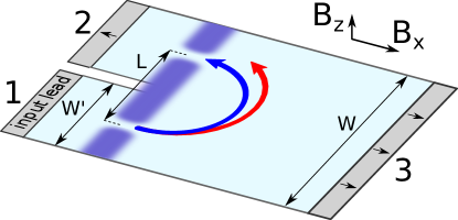
We consider quantum transport at the Fermi level in 2DEG confined within an InSb quantum well. The model system depicted in Fig. 1 contains two QPCs on the left-hand side, and is open on the right-hand side. The electrostatically defined two quantum point contacts are separated by a distance . The terminals are numbered as indicated in Fig. 1. The electrons entering from the lead 1 are injected trough the first (lower) QPC into the system in a narrow beam that is steered by the transverse magnetic field. Whenever the cyclotron diameter (or its integer multiple) fits the separation , electrons can enter the second QPC which serves as a collector. Electrons that do not get to the collector exit the system through the lead 3, which is used as open boundary conditions. Hard wall boundary conditions are introduced on the perpendicular edges of the computational box. The size of the computational box (width nm and length 1800 nm) is large enough to make the effects of the scattering by the hard wall boundaries negligible for the drain (lead 2) currents.
For the transport modeling, we assume that the vertical confinement in the InSb quantum well is strong enough to justify the two-dimensional approximation for the electron motion. The 2D effective mass Hamiltonian reads
| (1) |
where , with being the vector potential, , is the vector of Pauli matrices, is the Bohr magneton, is the diagonal Landé tensor, and is the electron effective mass in InSb.
.
The external potential as seen by the Fermi level electrons is a superposition of the QPC and the potential induced by the charged SGM tip
| (2) |
where we model the QPC using the analytical formulas developed in Davies et al. (1995) with electrostatic potential of a finite rectangular gate given by
| (3) |
where with nm, and is the potential applied to the gates. The QPC potential is a superposition of potentials of three such gates
| (4) |
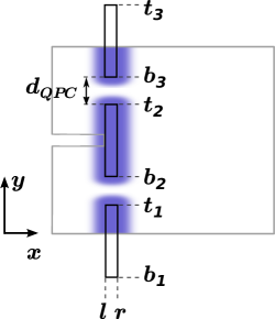
The gates and their labeling used in Eq. (4) are schematically shown in Fig. 2. The splitting of the gates is nm defining the QPC width. The QPCs are separated by nm.
For modeling the tip potential we use a Gaussian profile
| (5) |
with being the maximum tip potential, its width, and , the coordinates of the tip.
The spin-orbit interactions in InSb are strong, so we include them in the calculations. The two last terms in (1) account for the SOI with , where
| (6) |
describes the Rashba interaction, and
| (7) |
the Dresselhaus interaction. For the Hamiltonian (1) we use the parameters for InSb quantum well, eVÅ, eVÅ, Gilbertson et al. (2008), Qu et al. (2016), Qu et al. (2016).
We perform the transport calculations in the finite difference formalism. For evaluation of the transmission probability, we use the wave function matching (WFM) technique Kolasiński et al. (2016). The transmission probability from the input lead to mode with spin in the output lead is
| (8) |
where is the probability amplitude for the transmission from the mode with spin in the input lead to mode with spin in the output lead. We evaluate the conductance as , with .
The considered system presented in Fig. 1 has the width nm, and the narrow leads numbered 1 and 2 have equal width nm. The spacing between the centers of the QPCs is nm. We take the gate potential meV, for which at meV in the absence of the external magnetic field the QPC conductance is close to . For the SGM we use the tip parameters meV, and nm.
III Results
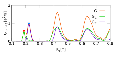
III.1 No in-plane magnetic field
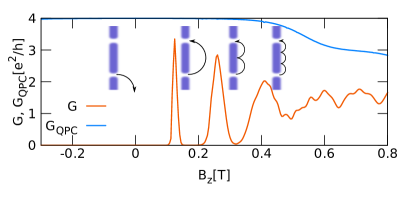
Let us first consider the transport in the system with the out-of-plane magnetic field only (i.e. , , ). In Fig. 3 we present the conductance from the lead 1 to lead 2 as a function of the applied transverse magnetic field, and the summed conductance from the lead 1 to the leads 2 and 3, which is essentially the conductance of the lower QPC . For no focusing peaks occur because the electrons are deflected in the opposite direction than the collector, propagate along the bottom edge of the system and finally exit through the right lead. For conductance peaks almost equidistant in magnetic field appear. The first three maxima occur at T, T, T. Neglecting the SOI terms and the Zeeman term in (1), one obtains . For the cyclotron diameter equal to
| (9) |
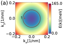
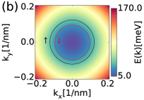
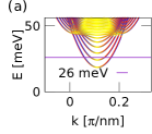
one obtains for the first three peaks nm, nm, nm, respectively. This is close to the distance between the centers of the QPCs, 1200 nm, its half , 600 nm, and one third, 400 nm, respectively. Despite the high spin-orbit interaction in the InSb quantum well, no spin splitting occurs. Let us denote the Fermi wave number of the subband of spin by . For the adapted values of the SO parameters, the difference in momenta for both spins is small [see Fig. 4(a)]. For example for and meV, the components extracted from the dispersion relation in Fig. 4(a) are nm-1, and nm-1, that for nm yield transverse magnetic field T and T, respectively. That is clearly too small difference to obtain a visible double peak.
III.2 Enhancement of the Zeeman splitting with in-plane magnetic field
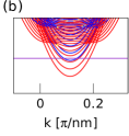
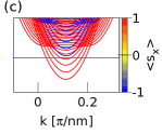
In the next step we apply an additional in-plane magnetic field. This leads to an increase of the Zeeman energy splitting for both spins leading to the increase of the momenta difference between both spin subbands. Fig. 4 shows the momenta for both spins for and 8 T. Without in-plane magnetic field, the spin subbands are nearly degenerate. With of the order of a few tesla the difference in the momenta becomes significant. This induces a change of the cyclotron radii of the electrons with opposite spins.
The spins are oriented along the total magnetic field, , where is the effective SO field. For of the order of a few tesla the out-of-plane magnetic field component and the SO effective field are small compared to the in-plane component. The spin is oriented nearly along the or direction. We refer to these states as spin-up and spin-down.
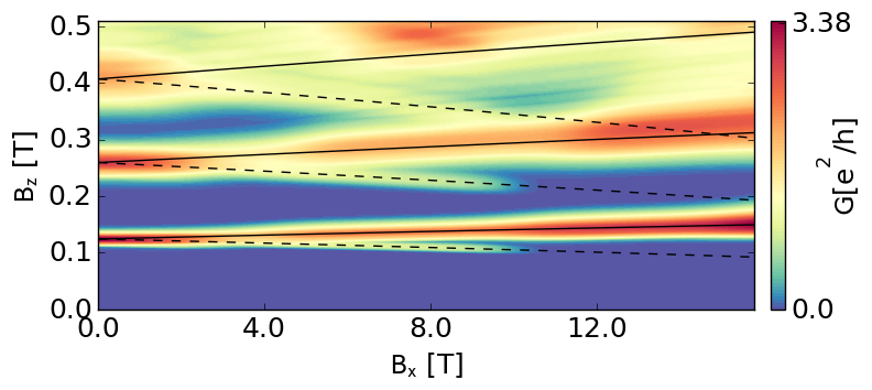
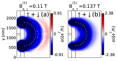
Fig. 5 shows the conductance from the lead 1 to the lead 2 as a function of the in-plane (here ) and the transverse magnetic fields. For sufficiently high in-plane magnetic field the peaks split, with the splitting growing with increasing . The lines plotted along the -th pair of split peaks are calculated from the condition , with obtained from
| (10) |
where , the sign corresponds to spin down and up, respectively, and are extracted from Fig. 3, using Eq. (9). Although the analytical lines are obtained neglecting the SOI and the Zeeman energy contribution from the transverse magnetic field, there is a good agreement between the obtained transport results and this simplified model.
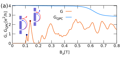
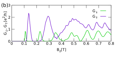
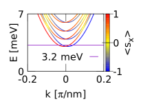
The cross section of the summed conductance and the spin-resolved conductance for T is shown in Fig. 6. In the pairs of focusing peaks, the spin-down (spin-up) conductance dominates for the peak at lower (higher) magnetic field [see Fig. 6(b)]. Interestingly, in each pair of the peaks in Fig. 5, the lower one has smaller transmission than the upper one, and at T vanishes, while the transmission of the upper one slowly increases. The reason for this behavior is the strong Zeeman splitting due to the in-plane magnetic field and the spin-dependent conductance of the QPCs Potok et al. (2002); Hanson et al. (2003). Fig. 7 shows the dispersion relation of an infinite channel with the lateral potential taken at the QPC constriction with applied , 8 T and 12 T. For T at the Fermi level for spin up 3 transverse subbands are available, while for spin down only one. For higher T the spin-down subband is raised above the Fermi level, and only spin-up electrons can pass through the QPC. On the other hand, for growing , the number of spin-up subbands increases. Thus in the focusing spectrum, the upper peak – the spin-up peak – becomes more pronounced, while the lower one – the spin-down peak – has lower value of transmission and finally disappears.
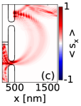
Concluding this section, we find that the in-plane magnetic field allows for a controllable separation of the electrons with opposite spins. It is worth noting that in the systems that have strong SOI, without the in-plane magnetic field, only the odd focusing peaks get split Usaj and Balseiro (2004); Reynoso et al. (2008b); Lo et al. (2017), and in case of the in-plane magnetic field all of the peaks are split. This is caused by the spin precession due to SOI in those systems. In our case the spin is determined by the effective magnetic field, which is almost parallel to direction. Thus the spin in direction dominates and the fluctuation due to SOI is negligible. It is shown in a representative case of the density and average spins for the low-field focusing peak at T in Fig. 8. The electron spins are nearly unchanged along the entire path. The and are negligibly small compared to the .
III.3 Scanning gate microscopy of the trajectories
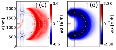
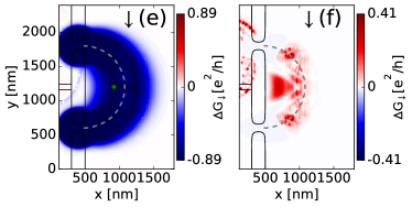
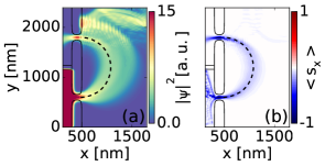
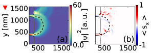
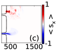
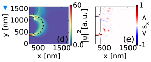
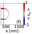
We simulated the SGM conductance maps for the magnetic fields that correspond to the peaks of magnetic focusing in the absence of the tip. We used T. In the cross section for T in Fig. 6(a) the dots show where the SGM scans were taken. Fig. 9 presents the maps of , and the spin-resolved conductances with . The conductance maps exhibit semicircular pattern with a pronounced minimum along the semi-classical orbit of a carrier incident in the direction (indicated in Fig. 9 with dashed semi-circles). For the spin-up focusing peak at T, the scan [Fig. 9(a)] is slightly different than for the spin-down peak at T [Fig. 9(b)]. In the first one there is a slight increase of conductance to the right of the dashed semi-circle [see the red blob in Fig. 9(a)]. Fig. 9(c,d) show the spin-up conductance, and Fig. 9(e,f) the spin-down conductance as a function of the tip position. One can see that in the spin-down peak (for T) the is everywhere negative or zero [Fig. 9(e)], and – positive or zero almost everywhere (except within the QPC) [Fig. 9(c)]. Examples of electron densities with the tip placed in two different points are shown in Fig. 10. In Fig. 10(a), the tip, when placed along the electron trajectory leads to the deflection of the beam and blocks the spin-down beam, preventing it from entering the collector. On the other hand, in Fig. 10(b), the tip can deflect the beam of spin-up electrons into the collector.
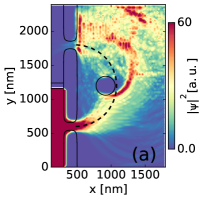
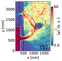
The situation is inverted in the peak at T. In the map [Fig. 9(d)], the values are smaller or equal to zero, and in the map [Fig. 9(f)], bigger or equal zero. In this case, the spin-up beam is blocked by the tip, thus drops along the semi-circle marked in Fig. 9(d). On the other hand, the spin-down electrons have a smaller cyclotron diameter [than the QPC spacing ], but they can be scattered by the tip to the collector, which leads to an increase of at some points to the left of (or along) the dashed semi-circle.
III.4 Magnetic focusing for heavy holes in GaAs/AlGaAs heterostructure
We consider an experiment conducted for two-dimensional hole gas (2DHG) in GaAs/AlGaAs, in Ref. Rokhinson et al., 2004, where the splitting of the first focusing peak was visible without an in-plane magnetic field, and was solely due to the spin-orbit interaction. For this problem we assume the distance between the two QPCs nm, the computational box of width nm and length nm, the QPC defined in the same manner as in Eq. 4 with the geometrical parameters: nm, nm, nm, nm, nm, nm, nm, nm, and =20 nm. We employ the effective mass of heavy holes Plaut et al. (1988), Landé factor Arora et al. (2013), the Dresselhaus SO parameter eVÅ Rokhinson et al. (2004), and zero Rashba SO.
We tune the lower QPC to , with meV, and meV. Figure 11 shows the focusing conductance of the system. The focusing peaks are resolved, with the first peak split by 35 mT, remarkably close to the result in Ref. Rokhinson et al., 2004, with the measured splitting of 36 mT. The splitting is due to the Dresselhaus SOI, which leads to the spin-polarization in the direction dependent on the hole momentum, and the difference in the Fermi wavenumbers of the holes with opposite spins. The band structure in the injector QPC is shown in Fig. 12. The hole spin in the injector QPC is in the direction.
The difference in focusing magnetic field due to SOI can be evaluated by:
| (11) |
The density and the spin evolution in the peaks highlighted in Fig. 11 by tiny triangles is shown in Fig. 13. In the densities [Fig. 13(a,d)] the contributions of both spins with slightly different cyclotron radii are visible. In the averaged spin component maps for the mode injected with spin up [Fig. 13(b,e)] the precession is visible, but a little blurred due to the scattering from the gates’ potential. For the mode injected with spin down [Fig. 13(c,f)] the flip of the spin direction in the detector is clearly visible.
IV Summary and Conclusions
We have studied the spatial spin-splitting of the electron trajectories in the transverse focusing system. We demonstrated that the in-plane magnetic field of a few tesla in InSb induces the Zeeman splitting which is large enough to separate the conductance focusing peaks for the spin-down and spin-up Fermi levels. The orientation of the spin is translated to the position of the conductance peak on the magnetic field scale. The focused trajectories for both the spin orientations can be resolved by the scanning gate microscopy conductance maps. Moreover, the SGM maps for opposite spin peaks contain qualitative differences due to the spin dependence of the cyclotron radii. The present finding paves the way for studies of the spin-dependent trajectories in the systems with the two-dimensional electron gas with high Landé factor materials.
Acknowledgments
This work was supported by the National Science Centre (NCN) Grant No. DEC-2015/17/N/ST3/02266, and by AGH UST budget with the subsidy of the Ministry of Science and Higher Education, Poland with Grant No. 15.11.220.718/6 for young researchers and Statutory Task No. 11.11.220.01/2. The calculations were performed on PL-Grid and ACK CYFRONET AGH Infrastructure.
References
- Wolf et al. (2001) S. A. Wolf, D. D. Awschalom, R. A. Buhrman, J. M. Daughton, S. von Molnár, M. L. Roukes, A. Y. Chtchelkanova, and D. M. Treger, Science 294, 1488 (2001).
- Sharvin (1965) Y. V. Sharvin, Sov. Phys. JETP 21, 655 (1965).
- Tsoi (1974) V. Tsoi, JETP Lett. 19, 70 (1974).
- van Houten et al. (1989) H. van Houten, C. W. J. Beenakker, J. G. Williamson, M. E. I. Broekaart, P. H. M. van Loosdrecht, B. J. van Wees, J. E. Mooij, C. T. Foxon, and J. J. Harris, Phys. Rev. B 39, 8556 (1989).
- Hanson et al. (2003) R. Hanson, B. Witkamp, L. M. K. Vandersypen, L. H. W. van Beveren, J. M. Elzerman, and L. P. Kouwenhoven, Phys. Rev. Lett. 91, 196802 (2003).
- Aidala et al. (2007) K. E. Aidala, R. E. Parrott, T. Kramer, E. J. Heller, R. M. Westervelt, M. P. Hanson, and A. C. Gossard, Nat. Phys. 3, 464 (2007).
- Dedigama et al. (2006) A. Dedigama, D. Deen, S. Murphy, N. Goel, J. Keay, M. Santos, K. Suzuki, S. Miyashita, and Y. Hirayama, Physica E Low Dimens. Syst. Nanostruct. 34, 647 (2006).
- Lo et al. (2017) S.-T. Lo, C.-H. Chen, J.-C. Fan, L. W. Smith, G. L. Creeth, C.-W. Chang, M. Pepper, J. P. Griffiths, I. Farrer, H. E. Beere, G. A. C. Jones, D. A. Ritchie, and T.-M. Chen, Nat. Commun. 8, 15997 (2017).
- Yan et al. (2017) C. Yan, S. Kumar, M. Pepper, P. See, I. Farrer, D. Ritchie, J. Griffiths, and G. Jones, Nanoscale Res. Lett. 12, 553 (2017).
- Rokhinson et al. (2004) L. P. Rokhinson, V. Larkina, Y. B. Lyanda-Geller, L. N. Pfeiffer, and K. W. West, Phys. Rev. Lett. 93, 146601 (2004).
- Chesi et al. (2011) S. Chesi, G. F. Giuliani, L. P. Rokhinson, L. N. Pfeiffer, and K. W. West, Phys. Rev. Lett. 106, 236601 (2011).
- Rokhinson et al. (2006) L. P. Rokhinson, L. N. Pfeiffer, and K. W. West, Phys. Rev. Lett. 96, 156602 (2006).
- Sellier et al. (2011) H. Sellier, B. Hackens, M. G. Pala, F. Martins, S. Baltazar, X. Wallart, L. Desplanque, V. Bayot, and S. Huant, Semicond. Sci. Technol. 26, 064008 (2011).
- Usaj and Balseiro (2004) G. Usaj and C. A. Balseiro, Phys. Rev. B 70, 041301 (2004).
- Zülicke et al. (2007) U. Zülicke, J. Bolte, and R. Winkler, New Journal of Physics 9, 355 (2007).
- Reynoso et al. (2007) A. Reynoso, G. Usaj, and C. A. Balseiro, Phys. Rev. B 75, 085321 (2007).
- Schliemann (2008) J. Schliemann, Phys. Rev. B 77, 125303 (2008).
- Reynoso et al. (2008a) A. A. Reynoso, G. Usaj, and C. A. Balseiro, Phys. Rev. B 78, 115312 (2008a).
- Kormányos (2010) A. Kormányos, Phys. Rev. B 82, 155316 (2010).
- Bladwell and Sushkov (2015) S. Bladwell and O. P. Sushkov, Phys. Rev. B 92, 235416 (2015).
- Yan et al. (2018a) C. Yan, S. Kumar, M. Pepper, K. Thomas, P. See, I. Farrer, D. Ritchie, J. Griffiths, and G. Jones, J. Phys. Conf. Ser. 964, 012002 (2018a).
- Kohda et al. (2012) M. Kohda, S. Nakamura, Y. Nishihara, K. Kobayashi, T. Ono, J.-i. Ohe, Y. Tokura, T. Mineno, and J. Nitta, Nature Communications 3, 1082 (2012).
- Zeng and Liang (2012) M. Zeng and G. Liang, Journal of Applied Physics 112, 073707 (2012).
- Gupta et al. (2014) G. Gupta, H. Lin, A. Bansil, M. B. Abdul Jalil, C.-Y. Huang, W.-F. Tsai, and G. Liang, Applied Physics Letters 104, 032410 (2014).
- Meier et al. (2007) L. Meier, G. Salis, I. Shorubalko, E. Gini, S. Schön, and K. Ensslin, Nature Physics 3, 650 (2007).
- Reynoso et al. (2008b) A. Reynoso, G. Usaj, and C. Balseiro, in Quantum Magnetism, edited by B. Barbara, Y. Imry, G. Sawatzky, and P. Stamp (Springer, Dordrecht, 2008) p. 151.
- Watson et al. (2003) S. K. Watson, R. M. Potok, C. M. Marcus, and V. Umansky, Phys. Rev. Lett. 91, 258301 (2003).
- Li et al. (2012) J. Li, A. M. Gilbertson, K. L. Litvinenko, L. F. Cohen, and S. K. Clowes, Phys. Rev. B 85, 045431 (2012).
- Yan et al. (2018b) C. Yan, S. Kumar, K. Thomas, P. See, I. Farrer, D. Ritchie, J. Griffiths, G. Jones, and M. Pepper, J. Phys. Condens. Matter 30, 08LT01 (2018b).
- Wharam et al. (1988) D. A. Wharam, T. J. Thornton, R. Newbury, M. Pepper, H. Ahmed, J. E. F. Frost, D. G. Hasko, D. C. Peacock, D. A. Ritchie, and G. A. C. Jones, J. Phys. C 21, L209 (1988).
- van Wees et al. (1988) B. J. van Wees, H. van Houten, C. W. J. Beenakker, J. G. Williamson, L. P. Kouwenhoven, D. van der Marel, and C. T. Foxon, Phys. Rev. Lett. 60, 848 (1988).
- van Wees et al. (1991) B. J. van Wees, L. P. Kouwenhoven, E. M. M. Willems, C. J. P. M. Harmans, J. E. Mooij, H. van Houten, C. W. J. Beenakker, J. G. Williamson, and C. T. Foxon, Phys. Rev. B 43, 12431 (1991).
- Qu et al. (2016) F. Qu, J. van Veen, F. K. de Vries, A. J. A. Beukman, M. Wimmer, W. Yi, A. A. Kiselev, B.-M. Nguyen, M. Sokolich, M. J. Manfra, F. Nichele, C. M. Marcus, and L. P. Kouwenhoven, Nano Lett. 16, 7509 (2016).
- LeRoy et al. (2005) B. J. LeRoy, A. C. Bleszynski, K. E. Aidala, R. M. Westervelt, A. Kalben, E. J. Heller, S. E. J. Shaw, K. D. Maranowski, and A. C. Gossard, Phys. Rev. Lett. 94, 126801 (2005).
- Jura et al. (2009) M. P. Jura, M. A. Topinka, M. Grobis, L. N. Pfeiffer, K. W. West, and D. Goldhaber-Gordon, Phys. Rev. B 80, 041303 (2009).
- Paradiso et al. (2010) N. Paradiso, S. Heun, S. Roddaro, L. Pfeiffer, K. West, L. Sorba, G. Biasiol, and F. Beltram, Physica E Low Dimens. Syst. Nanostruct. 42, 1038 (2010).
- Brun et al. (2014) B. Brun, F. Martins, S. Faniel, B. Hackens, G. Bachelier, A. Cavanna, C. Ulysse, A. Ouerghi, U. Gennser, D. Mailly, S. Huant, V. Bayot, M. Sanquer, and H. Sellier, Nat. Commun. 5, 4290 (2014).
- Crook et al. (2003) R. Crook, C. G. Smith, A. C. Graham, I. Farrer, H. E. Beere, and D. A. Ritchie, Phys. Rev. Lett. 91, 246803 (2003).
- Burke et al. (2010) A. M. Burke, R. Akis, T. E. Day, G. Speyer, D. K. Ferry, and B. R. Bennett, Phys. Rev. Lett. 104, 176801 (2010).
- Crook et al. (2000) R. Crook, C. G. Smith, M. Y. Simmons, and D. A. Ritchie, Phys. Rev. B 62, 5174 (2000).
- Morikawa et al. (2015) S. Morikawa, Z. Dou, S.-W. Wang, C. G. Smith, K. Watanabe, T. Taniguchi, S. Masubuchi, T. Machida, and M. R. Connolly, Appl. Phys. Lett. 107, 243102 (2015).
- Bhandari et al. (2016) S. Bhandari, G.-H. Lee, A. Klales, K. Watanabe, T. Taniguchi, E. Heller, P. Kim, and R. M. Westervelt, Nano Lett. 16, 1690 (2016).
- Davies et al. (1995) J. H. Davies, I. A. Larkin, and E. V. Sukhorukov, J. Appl. Phys. 77, 4504 (1995).
- Gilbertson et al. (2008) A. M. Gilbertson, M. Fearn, J. H. Jefferson, B. N. Murdin, P. D. Buckle, and L. F. Cohen, Phys. Rev. B 77, 165335 (2008).
- Kolasiński et al. (2016) K. Kolasiński, B. Szafran, B. Brun, and H. Sellier, Phys. Rev. B 94, 075301 (2016).
- Potok et al. (2002) R. M. Potok, J. A. Folk, C. M. Marcus, and V. Umansky, Phys. Rev. Lett. 89, 266602 (2002).
- Plaut et al. (1988) A. S. Plaut, J. Singleton, R. J. Nicholas, R. T. Harley, S. R. Andrews, and C. T. B. Foxon, Phys. Rev. B 38, 1323 (1988).
- Arora et al. (2013) A. Arora, A. Mandal, S. Chakrabarti, and S. Ghosh, J. Appl. Phys. 113, 213505 (2013).