Spin signatures in the electrical response of graphene nanogaps
Abstract
We analyse the electrical response of narrow graphene nanogaps in search for transport signatures originated from spin-polarized edge states. We find that the electrical transport across graphene nanogaps having perfectly defined zigzag edges does not carry any spin-related signature. We also analyse the magnetic and electrical properties of nanogaps whose electrodes have wedges that possibly occur in the currently fabricated nanogaps. These wedges can host spin polarized wedge low-energy states due to the bipartite nature of the graphene lattice. We find that these spin-polarized low-energy modes give rise to low-voltage signatures in the differential conductance and to distinctive features in the stability diagrams. These are originated by fully spin-polarized currents.
I Introduction
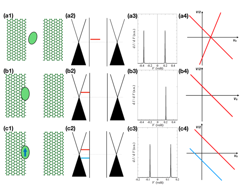
The development of graphene-based nano-electronics requires the fabrication of well-controlled nanometer-scale gaps. Graphene nanogaps with gap lengths of the order of one to few nanometres have indeed been realized in the past few years, via electro-burning techniquesPrins et al. (2011a); Nef et al. (2014); Gehring et al. (2016); El Abbassi et al. (2017). Very recently, graphene nanogaps have been fabricated via the Mechanically Controlled Break Junction technique Caneva et al. (2018). However, while these nano-gaps have indeed a length in the nanometer range, control over their morphology and content of the resulting edges is still in its infancy. Indeed, the differential conductance of the nano-gaps presents frequently a low-voltage resonance peak that is also manifested as a cross in the stability diagram (i.e.: a plot of the bias versus the gate voltage ), as we depict schematically in the first row of Figure 1. This resonant tunnelling behaviour is possibly due to molecular species left inside the nanogap by the electro-burning process. A possible question that may arise is whether localized electronic states at the edges can also lead to non-trivial tunnelling features. These features could only be measured above the electrical noise if the nanogap is as short as half a nanometer, or whether the localized state protrudes enough from the edge. This scenario is depicted in the second and third rows of Figure 1, that correspond to a non-magnetic and a magnetic state, respectively. We analyse in this article situations where this third scenario may be realized.
In the first situation, the graphene sheets at the nano-gap are terminated by hydrogenated zigzag graphene edges, that are predicted to carry spin polarized states with a local moment at the carbon edge atom aproaching 1/3 Fujita et al. (1996); Lehtinen et al. (2003); Son et al. (2006); Pisani et al. (2007); Yazyev and Helm (2007); Yazyev (2010); Li et al. (2013); Meunier et al. (2016). Experimental evidence of the existence of these spin-polarized edge states has emerged only recently Tao et al. (2011); Baringhaus et al. (2014); Slota et al. (2018) In the second and more realistic situation, we assume that one of the edges shows a protuberance in the form of a wedge, as we depict in Figure 2. Vacancies, voids, islands of different shapes or wedge-terminated edges have also been predicted to display local magnetic momentsLieb (1989); Fernández-Rossier and Palacios (2007); Palacios et al. (2008); Carrascal et al. (2012); Lado et al. (2016). Spin-polarized localized states in graphene sheets have been recently demonstrated via hydrogen decorationGonzález-Herrero et al. (2016), while nano-scale graphene islands passivated with hydroxyl groups have also been found to be magnetic Sun et al. (2017). We analyse in this article simple hydrogen passivation as a representative example, although we will also show some results for hydroxyl passivation of isolated graphene islands.
Magnetism at graphene edges can arise if the dangling bonds of the edge carbons are saturated with chemical groups so that they retain the bipartite nature of the original lattice and its half-filling naturePalacios and Ynduráin (2012). In addition, the pz orbitals at the edges must remain not fully saturated. This can be achieved not only by simple hydrogen passivation, but also by passivation via hydroxyl, carboxyl and COO groupsSun et al. (2017); Zhao et al. (2014). Under these conditions, the sheets can be described to a first approximation by the half-filled Hubbard model on a bipartite lattice and Lieb’s theorem appliesLieb (1989). This theorem states that if a bipartite lattice has and A and B sites so that there is a net unbalance , then the ground state has a moment . Additionally, the energy spectrum displays zero-energy modes, that are spin-split symmetrically about the Fermi energy by an amount that is proportional to the on-site Coulomb repulsion Palacios et al. (2008); Mielke (2015); Asboth et al. (2016). The occupied spin-up modes give rise to the finite moment predicted by Lieb’s theorem.
We analyse first nanogaps containing two hydrogenated zigzag edges, that carry spin polarized edge states, that we call in this article ZZ nanogaps. We find that the magnetic anisotropy of the spin-polarized edge states is consistent with a zero value and that their exchange coupling across the gap is minute and has a very short decay length. In consequence, the edge spin states show Heisenberg super-paramagnetic behaviour at any relevant laboratory temperature. This means that graphene nanogaps cannot show magnetorresistive behaviour. We also find that the differential conductance across these ZZ nanogaps is featureless and therefore does not carry any spin signature. We also find that the tunnelling decay length across the gap Å, i.e.: is smaller than the Bohr radius. This important fact indicates that the electrical transport across a short-length nanogap must be dominated by those protrusions having a height larger than about Å.
This is the reason why we turn to analyse in the second place nanogaps where one electrode displays a protrusion or wedge with a sub-lattice unbalance equal or larger than three or four, as is the case of Figure 2. These are called WZ nanogaps in the present article. We find, in agreement with previous work Fernández-Rossier and Palacios (2007); Palacios et al. (2008); Carrascal et al. (2012), that these electrodes display a magnetic moment localized at the wedge whose magnitude obeys Lieb’s theoremLieb (1989). We find low energy, single-electron spin-polarized states localized at the wedge. One of these spin-polarized states is placed at the wedge tip and gives rise to a single pair of low-voltage peaks in the differential conductance, as shown in bottom row of Figure 1. We finally analyse WW nanogaps where two protrusions are roughly facing each other. These nanogap configurations display a more complex electrical response. We however expect that most experimental nanogaps should be of the WZ kind because the very short tunnelling decay length.
We show finally some experimental differential conductance d/d traces that we have measured across several nanometer-size gaps, that show a pair of peaks. These measurements are consistent with the response of the WZ nanogaps discussed in the article, but also with the more conventional resonant tunnelling scenario shown in the top row of Figure 1. We expect that the technology for nanogap fabrication will undergo a substantial development in the near future, and that control over the morphology of graphene edges as well as edge decoration may be attained in due time. We therefore propose the mechanism laid in this article as a simple means to produce fully spin polarized electrical currents in a nanogap setting.
II Results and Discussion
II.1 Electrical response of a ZZ nanogap
The electronic and magnetic properties of hydrogenated zigzag nanoribbons have been discussed extensively in the past. We have therefore relegated our Density Functional Theory calculations on the matter to the Supporting Information, together with a few new results, that we summarize here. We find that the magnetic anisotropy energy of the edge zigzag states is of order or smaller than 0.01-1 eV, actually consistent with a value of zero. We therefore expect that edge-state spin coherent dynamics be driven by coherent rotation processes. We show in Figure 3 (a) the band structure and the Density of States of a zigzag ribbon that features two peaks corresponding to the spin-polarized edge states.
We make now a ZZ nanogap based on the above ribbon to compute the transport properties across the gap. We have first estimated the exchange interaction across the nanogap and found it to be as small as
| (1) |
so that we expect that the spin alignment of the edge states at both sides of the junction will be fluctuating between parallel (P) and anti-parallel (AP) configurations at any laboratory temperature. The DOS of each sheet is plotted in Figure 3 (b) in a narrow energy window where we focus on the peaks originated by the edge states, that are still there. The Open Channels are an intrinsic property of each electrode, and measure the available number of conduction channels at a given energy that the electrons can use to impinge onto a scattering region, i.e.: the gap in our case. Figure 3 (c) shows that the for our graphene electrodes possess electron-hole symmetry and are spin-unpolarized. Figure 3(d) shows that the peaks in the DOS do not translate into peaks in the spin-resolved transmission . This curve therefore demonstrates that the edge states do not contribute to the electrical transport across the gap. Furthermore, we have computed the spin-resolved transmission function for the parallel (P) and anti-parallel (AP) spin alignments of the edge states. We have found that is featureless for both spin alignments in the energy window shown in the Figure. We have also found that for the AP alignment is exactly the average of and for the P alignment, yielding a theoretical zero magnetorresistance ratio. The slopes of are different for positive and negative energies, reflecting a slight loss of electron-hole symmetry. This is remarkable because an inspection to the bulk graphene conduction channels reveals that these are electron-hole symmetric.
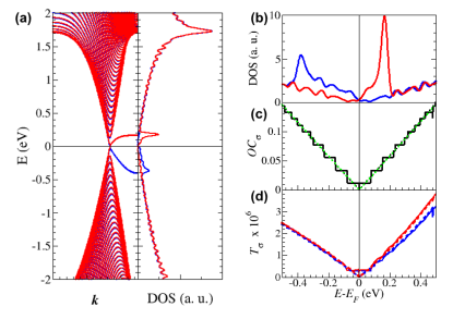
The featureless differential conductance of a ZZ nanogap enables us to determine unambiguously the dependence of on the gap length , measured as the distance between the hydrogen atoms on both edges. We find that the zero-bias conductance shows the expected exponential decay, i.e. , with a tunnelling decay length Å i.e.: smaller than a Bohr radius. This tiny decay length means that a ZZ nanogap should display negligible tunnelling current for nm or larger. It also means that the nanogap electrical response should be dominated by the largest protrusion or wedge appearing at any of the two nanogap edges. To place this statement on a firmer ground, we estimate the current flowing through a WZ nanogap where one of the two edges has a wedge having two extra rows. This means that the carbon atom at the wedge tip is Å closer to the opposite electrode than the outermost carbon atoms at the adjacent zigzag segments. Using the above decay length, we estimate that the contribution of this tip atom to the tunneling current is times larger than the contribution of carbon atoms at the zigzag segments, meaning that the wedge contribution dominates the gap conductance.
II.2 Properties of triangular islands
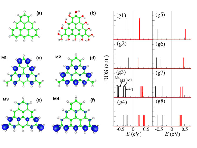
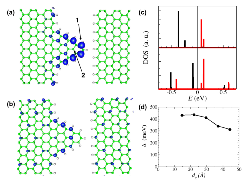
We discuss now the properties of graphene islands having a shape similar to the wedges. We show in Figure 4 (a), (b) two islands that have rows. They have an unbalance and , respectively. We have passivated the two islands with hydrogen or with hydroxyl groups, and use the notation R4I2H, R4I2OH, R4I4H or R4I4OH, respectively. Similar structures with unsatured carbon pz orbitals at the edges were addressed a few years ago in references Fernández-Rossier and Palacios, 2007; Palacios et al., 2008, and we recapitulate here some rules relevant for the present work: (1) The structures are well represented by the half-filled Hubbard model in a bipartite lattice and therefore satisfy Lieb’s theoremLieb (1989); (2) the single-particle spectrum of the structure has zero-energy states per spin channel, that are exchange split as ) ; (3) because there are electrons available, the resulting state has a moment . We have verified that the moment is for the four islands in accordance with Lieb’s theorem Lieb (1989), and that each island has modes having spin 1/2, each of them split by , as we show in Figure 4 (g1)-(g8), where we plot the Density of States (DOS) of the islands in the neighbourhood of the Fermi level. We have placed the modes split symmetrically about the Fermi energy to aid the eye and to connect with the conclusions drawn for the Hubbard model Fernández-Rossier and Palacios (2007). The splitting depends on the kind of passivation: we find that hydroxyl groups yield a smaller splitting than hydrogen atoms. In addition, this spin splitting is inversely proportional to the island’s size, as we show in the Figure (see also Ref. Palacios et al., 2008). We focus now in the R4I4H island (Figure 4 (g3)), whose shape is closest to the wedges in this article. This island has four low-energy modes, that we call M1, M2, M3 and M4. We find that their degeneracy is broken because of island’s lower symmetry, as shown in Figure 4 (g3). The four states of the spin-down DOS are quasi-degenerate, and the spin-splitting is of eV. Figure 4 (c)-(f) shows the spin-up Local Density of States (LDOS) of each mode M1-M4. They have a distinct shape and location across the island that will be reflected later on in their specific contribution to the electrical transport across WS gaps.
II.3 Magnetism and zero-energy modes of graphene wedges
We aim at describing now the properties of semi-infinite sheets whose single edge has a triangular wedge attached to it having rows as in Figure 5 (a). This wedges are similar in shape to the islands in Figure 4 (b). We set a nanogap length nm, long enough to avoid any interaction across the nanogap. By construction, the sublattice unbalance of these single-wedge nanogaps is , and we have checked that our DFT calculations yield a ground state with as expected. We analyse in detail the wedge for the sake of concreteness. The wedge hosts low-energy modes whose LDOS look similar to those shown in Figure 4 (c)-(f), as expected. We plot the spin-resolved DOS projected onto atoms 1 and 2 at the wedge tip in Figure 5 (c) . We find that the low-energy PDOS at atom 1 is dominated by a single spin-split mode that we identify as the M1 mode of the equivalent island. To confirm this assertion, we show in Figure 5 (a) the spin-up LDOS of the M1 mode, that looks extremely similar to that in Figure 4 (c). It also shares a similar, somewhat smaller, spin-splitting eV. The PDOS projected onto atom 2, that we show in Figure 5 (c), shows that the M2 mode splits into two peaks. This is due to hybridization with the bulk graphene modes. This can be seen by looking at the LDOS of each of the two split spin-up peaks. We show the one corresponding to the peak at -0.5 eV in Figure 5 (b). Because of this hybridization the spin-splitting is smaller, of order 0.1 eV. We find that the other two modes are localized away from the wedge tip, and closer to the semi-infinite sheet.
However, the energy of the wedge modes is not placed symmetrically about the Fermi energy, losing the spin-resolved electron-hole symmetry. For example, we find that eV and eV. This symmetry loss is physical and due to the electron-hole symmetry loss inherent in the DFT hamiltonian. We note that electron-hole symmetry is lost in a bi-partite lattice by adding hopping or Coulomb interaction matrix elements linking atoms in the same sub-lattice (i.e.: second nearest neighbours, see the extended Hubbard model discussed in the Supplementary Information).
We note that a real electrode has many protrusions at its edge. As demonstrated above, we expect that one of these protrusions will dominate the tunneling current. For discussion, we assume that the dominating wedge is a wedge. We find below that only the M1 mode gives rise to a low-voltage conductance peak in our transport simulations, that appears at a voltage , so we focus from now on on this mode and on its spin-splitting. We have found above that depends on the kind of carbon passivation, being larger for hydrogen than for hydroxyl passivation. We have also found that it is inversely proportional to the wedge size. However, may depend also on the distance between the dominating wedge and its closest cousin. We have estimated , via our simulations of a WZ nanogap, where we vary the height Å of the unit cell. The bottom panel in Figure 5 shows our results for the discussed wedge. This wedge has a length of about 12 Å at the base, so the first few distances correspond to the ”near field” interaction. While we do not have enough data points to attempt fitting the curve, we notice that the behaviour is consistent with a ”far field” interaction law
| (2) |
where meV and an exponent .
II.4 Electrical response of a WZ nanogap
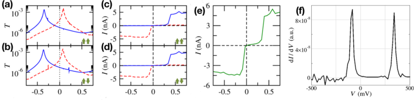
We discuss now the electrical response of WZ nanogaps, where we illustrate our results with the WZ nanogap shown in Figure 5. We have set the gap length nm so that the apparent length is nm. We fix the wedge spin in the up-direction, and orient the spin of the right-electrode zigzag edge upwards or downwards. Figures 6 (a) and (b) show that the spin-resolved transmissions for P and AP edge state spin alignments of the two electrodes are exactly the same. Therefore, we demonstrate again that the spin-polarized edge state at the right zigzag edge does not contribute to the electrical transport. The Figure also shows a single low-energy spin-split resonance, that appears exactly at the energy for the corresponding spin component. This corresponds to electron tunneling from the M1 mode at the wedge to the continuum of bulk states at the right electrode. The other wedge modes are localized further inside the wedge and deliver a negligible contribution to the electrical current. We have simulated WZ nanogaps with different , and have found that the height and width of the transmission resonance is proportional to the size of the wedge.
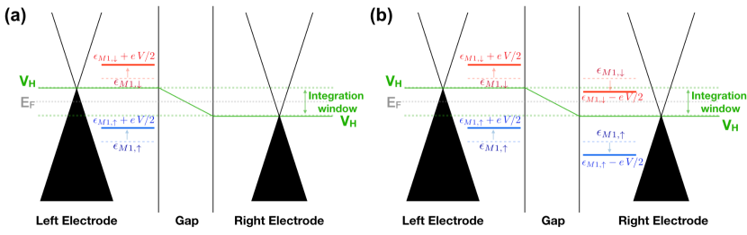
To understand the current-voltage curves, we draw the energy-level diagram shown in Figure 7 (a). The spin-split resonances corresponding to the M1 mode are localized in the wedge, i.e.: at the left electrode. They are centred at at zero voltage and do not possess electron-hole symmetry as discussed above. These two resonances shift up in energy when a positive bias voltage is applied according to . Therefore only the (negative-energy) spin-up resonance enters the integration window for positive bias. This happens at the threshold voltage , resulting in a sudden jump on the current, that is fully spin-up polarized. The resonance stays inside the integration window upon further increase of the bias voltage, and as a consequence the current remains constant. Conversely, only the (positive-energy) spin-down resonance enters the integration window at negative bias at resulting in a fully polarized spin-down current. The resulting spin-resolved and spin-summed current-voltage characteristics are shown in Figure 6 (c), (d) and (e), while the differential conductance is plotted in Figure 6 (f).
We mention that the application of a magnetic field modifies the energy of these spin 1/2 modes by the usual amount meV, where is measured in Tesla. This means that a magnetic field as large as 10 T shifts the modes by an amount of 0.5 meV.
II.5 Electrical properties of a WW nanogap
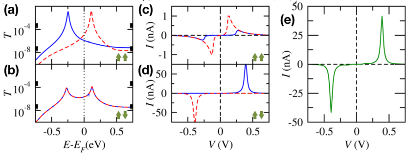
We discuss finally the electrical response of WW nanogaps where two wedges are facing each other across the gap. We have also simulated WW nanogaps where the two wedges are slightly shifted relative to each other, finding results similar to those discussed here if the two wedges are not strictly aligned. We find that the zero-voltage transmission coefficients for the P wedge alignment are similar to those of a WZ nanogap, having resonances at energies (see Figure 8 (a)). They correspond to tunneling between the M1 modes at both wedges as we show schematically in Figure 7 (b) for the P spin alignment. The low-voltage current is tiny because even though the two levels are aligned energetically, they stay outside the integration window. As the voltage is raised from zero, the two levels de-align. The spin-up M1 level at the left electrode never enters the integration window, while the right spin-up M1 level does enter at , resulting in a sudden rise of the current. This rise is small though because the two spin-up levels are de-aligned. Further increase of the voltage results in a Negative Differential Resistance feature because even though the right spin-up M1 level remains inside the integration window, the two levels de-align even further. The spin-resolved current-voltage curve for the P alignment is shown in Figure 8 (c).
The spin-up and -down M1 levels at the right electrode are swapped for the AP wedge alignment. As a consequence, the spin-up M1 levels at both wedges shift towards the Fermi level and enter the integration window when the bias voltage is increased from zero. Eventually they align with each other resulting in a large increase of the spin-up current. If the bias voltage is increased further then the two spin-up levels de-align and the current shrinks. The spin-down current is very small for positive biases because the spin-down levels at each side of the gap both move away from the integration window. Upon voltage reversal, the spin-up levels move away from the integration window, while the spin-down levels move towards it, eventually entering it and later on aligning with each other, resulting in a large increase of the spin-down voltage. The computed current-voltage is shown in Figure 8 (d). Perfect spin rectification and a large NDR signal is then expected for this nano-gap. The current peak for the AP is one order of magnitude larger than the current plateau for the P alignment. Because the nanogap follows super-paramagnetic behaviour, we expect that the AP current peak should dominate the current-voltage characteristics as we show in Figure 8 (e).
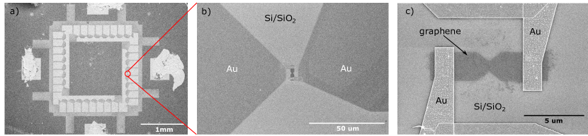
III Experimental measurements of graphene nanogaps
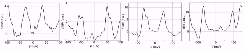
A set of nanometer-spaced graphene electrodes is prepared is prepared by electron-beam lithography and feedback-loop controlled electroburning of graphene Prins et al. (2011b); Burzurí et al. (2012); Island et al. (2014); Burzurí et al. (2016). A scanning electron microscope (SEM) image of the resulting devices is shown in Figure 9. Electron transport measurements across the gaps are performed at cryogenic temperatures ( around 2K) to reduce thermal noise. In particular, the electrical current is measured as a function of an applied bias voltage between the two graphene electrodes. The differential conductance d/d is thereafter numerically obtained. Some representative d/d characteristics measured in four devices are shown in Figure 10. These show low-voltage peaks in the 30-100 mV range, that are placed roughly symmetrically around zero voltage, however this symmetry is not exact. These results fit qualitatively with the theoretical differential conductance for a WZ nanogap and would point to one or more WZ edges participating in the electron transport across the gap. The results are also consistent with conventional resonant tunnelling by a single level placed inside the nanogap as shown in Figure 1 (a3).
IV Conclusions
We have proposed in this article two possible realizations of graphene nano-gaps that result is spin-polarized currents originated by spin-polarized low-energy modes residing on the electrodes protrusions. These spin-polarized states are zero-energy modes whose degeneracy is lifted by the Coulomb Hubbard interaction. We find that the fully spin-polarized might show perfect spin rectification together with low-voltage charge rectification. Additional features, like Negative Differential Resistance, that is spin-polarized should be an indication that two such protrusions are roughly facing each other. Our experimental measurements are consistent with our computational predictions for WZ nanogaps. We believe that further technological developments will enable to achieve a detailed control of the edges shape in nanogaps, so that our proposed mechanism can be used to design spintronically active devices.
V Methods
V.1 Technical details of the calculations
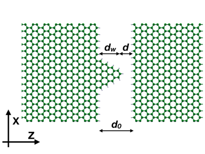
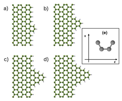
The super-cell used in our nanogap simulations is depicted schematically in Figure 2, where the X- and Z-axes are also shown. It consists of an hydrogenated ribbon whose edges run along the X-axis, are placed in the middle of the cell, and are separated by a gap of length . The elementary unit cell (EUC) used to build the nanogaps is shown in Figure 11 (e) and consists of four carbon atoms. The height of the super-cell has EUCs that corresponds to nm. Periodic boundary conditions are applied across the three spatial directions. The super-cell can be considered as a nanogap if is small enough that the wave functions at the two edges overlap with each other, or a ribbon in the opposite case. Several possible wedges for WZ nanogaps are illustrated in Figure 11 (a)-(d). They are characterized by the number of extra carbon rows , that correspond to a given wedge height . We note that the electrical current and conductance across the gap depend exponentially on the gap length but only linearly on the cross-sectional length. However, because the current is dominated by the wedge, the effective tunnelling length determined by a Simmons’ fitting Simmons (1963) of the tunnelling current and the apparent nanogap length estimated in a TEM image of the nanogap need not be the same. The strong dependence of the tunnelling current on conveys a large reduction of the effective cross-sectional length .
We have determined the magnetic properties of SS nanogaps through the Vienna Ab initio Simulation Package (VASP)Kresse and Hafner (1993); Kresse and Furthmüller (1996). The code expands the wave functions of the valence electrons in a plane-wave basis set where we have used an energy cutoff of 400 eV. Interactions among valence and core is reproduced with the Projector Augmented Wave (PAW) method Blöchl (1994); Kresse and Joubert (1999). We have used a Generalized Gradient Approximation functional Perdew et al. (1996). To find the optimal atomic arrangement we relaxed the inter-atomic forces using a force tolerance eV/Å. After force relaxation, we have included the Spin-Orbit interaction and have run the code again to determine the magnetic properties using 16 k-points along the X-axis. We have also used the code SIESTA to calculate magnetic moments and magnetic anisotropiesFernández-Seivane et al. (2006) and benchmark them against our VASP results. SIESTA uses norm-conserving pseudopotentials and linear combinations of atomic orbitals as basis set Soler et al. (2002). Because the above magnetic properties are rather sensitive to accuracy parameters, we have used a double-zeta polarized basis that includes d-orbitalsGmitra et al. (2009), a real-space mesh defined by a cutoff energy of 1000 Ry, an electronic tolerance for the density matrix of eV and a tolerance for the maximum atomic forces of eV/Å. We have simulated graphene islands with a triangular shape similar to the wedges. We have passivated the carbon atoms at the edges with hydrogen atoms or hydroxyl groups. We have used a double-zeta polarized supplemented with diffuse orbitals for all the islands’ atoms, and have relaxed all atomic forces below a tolerance of eV/Å.
We have determined the electronic properties of the different nanogaps mostly via SIESTA, where we have used a double-zeta basis set for the inner carbon atoms at the sheets. We have described the carbon and hydrogen atoms at the wedges and edges using a double-zeta polarized basis set that included diffuse orbitals with quite long radii. We have chosen a mesh cut-off of 300 Ry to define the real space grid and the LDA exchange and correlation functional Perdew and Zunger (1981). We have determined the electrical response of the nanogaps via the quantum transport code GOLLUM Ferrer et al. (2014). The code reads either DFT or model tight-binding Hamiltonians to generate those transport properties, and we have used the DFT code SIESTA in the present article. We have checked that the above-described basis set provides a reasonable description of the tunneling currents. Most of the calculations discussed here do not include transverse points.
V.2 Experimental details
The nanogaps are fabricated on chemical vapor deposited (CVD) graphene films grown on Si/SiO2 substrates. Tens of graphene bridges narrowed at the central part into bow-tie constrictions (m) are pre-patterned on the sheets by electron-beam lithography. The surrounding excess graphene is thereafter etched away with oxygen plasma reactive-ion etching. The electrical contact to the resulting graphene bridges is established through gold pads fabricated by electron-beam lithography and subsequent gold deposition. A scanning electron microscope (SEM) image of the resulting devices is shown in Fig. 9. The opening of the nanogaps is achieved via a feedback-loop controlled electroburning technique Prins et al. (2011b); Burzurí et al. (2012). A voltage bias in the few-volts range is applied between the Au terminals at room temperature and in air. The high current density generated heats the flake by Joule effect until eventually some carbon atoms are removed around the constriction where the heat dissipation efficiency is lower Island et al. (2014); Burzurí et al. (2016). As soon as the conductance drops around 10 %, the voltage is ramped to zero in milliseconds to avoid the abrupt burning of the flake that may result in wide gaps. The burning process is repeated until the low bias ( mV) resistance is greater than 10 G to avoid the presence of graphene nano-islands bridging the electrodes.
JF, AGF, VMGS and DC acknowledge funding by the Spanish MICINN through the grants FIS2012-34858 and FIS2015-63918-R. EB thanks funds from the EU FP7 program through Project 618082 ACMOL and the H2020-MSCA-IF 746579. Research at Delft was supported by NOW/OCW and an ERC advanced grant (Mols@Mols; HvdZ). Support by the EU FP7-ITN MOLESCO grant (no. 606728) and the EU H2020 RIA QuIET grant (no. 767187) is also gratefully acknowledged.
References
- Prins et al. (2011a) F. Prins, A. Barreiro, J. M. Ruitenberg, J. S. Seldenthius, N. Aliaga-Alcalde, L. M. K. Vandersypen, and H. S. J. van der Zant, Nano Lett. 11, 4607 (2011a), URL http://pubs.acs.org/doi/abs/10.1021/nl202065x.
- Nef et al. (2014) C. Nef, L. Pósa, P. Makk, W. Fu, A. Halbritter, C. Schoenenberger, and M. Calame, Nanoscale 6, 7249 (2014), URL http://pubs.rsc.org/en/Content/ArticleLanding/2014/NR/c4nr01838a#!divAbstract.
- Gehring et al. (2016) P. Gehring, H. Sadeghi, S. Sangtarash, C. S. Lau, J. Liu, A. Ardavan, J. H. Warner, C. J. Lambert, G. A. D. Briggs, and J. Mol, Nano Lett. 16, 4210 (2016), URL http://pubs.acs.org/doi/abs/10.1021/acs.nanolett.6b01104.
- El Abbassi et al. (2017) M. El Abbassi, L. Posa, P. Makk, C. Nef, K. Thodkar, A. Halbritter, and M. Calame, Nanoscale 9, 17312 (2017), URL http://dx.doi.org/10.1039/C7NR05348G.
- Caneva et al. (2018) S. Caneva, P. Gehring, V. M. Garcia-Suarez, A. García-Fuente, S. Davide, I. J. Olavarria-Contreras, J. Ferrer, C. Dekker, and H. S. J. van der Zant, arXiv:1803.05642 (2018), URL http://dx.doi.org/10.1039/C7NR05348G.
- Fujita et al. (1996) M. Fujita, K. Wakabayashi, K. Nakada, and K. K., J. Phys. Soc. Jap. 65, 1920 (1996).
- Lehtinen et al. (2003) P. O. Lehtinen, A. S. Foster, A. Ayuela, A. Krasheninnikov, K. Nordlund, and R. M. Nieminen, Phys. Rev. Lett. 91, 017202 (2003), URL http://journals.aps.org/prl/abstract/10.1103/PhysRevLett.91.017202.
- Son et al. (2006) Y. W. Son, M. L. Cohen, and S. G. Louie, Nature 444, 347 (2006), URL http://www.nature.com/nature/journal/v444/n7117/full/nature05180.html.
- Pisani et al. (2007) L. Pisani, J. A. Chan, B. Montanari, and N. M. Harrison, Phys. Rev. B 75, 064418 (2007), URL https://link.aps.org/doi/10.1103/PhysRevB.75.064418.
- Yazyev and Helm (2007) O. V. Yazyev and L. Helm, Phys. Rev. B 75, 125408 (2007), URL http://journals.aps.org/prb/abstract/10.1103/PhysRevB.75.125408.
- Yazyev (2010) O. V. Yazyev, Rep. Prog. Phys. 73, 056501 (2010), URL http://iopscience.iop.org/article/10.1088/0034-4885/73/5/056501.
- Li et al. (2013) Y. Li, W. Zhang, M. Morgenstern, and R. Mazzarello, Phys. Rev. Lett. 110, 216804 (2013), URL http://journals.aps.org/prl/abstract/10.1103/PhysRevLett.110.216804.
- Meunier et al. (2016) V. Meunier, A. G. Souza Filho, E. B. Barros, and M. S. Dresselhaus, Rev. Mod. Phys. 88, 025005 (2016).
- Tao et al. (2011) C. Tao, L. Jiao, O. V. Yazyev, Y.-C. Chen, J. Feng, X. Zhang, R. B. Capaz, J. M. Tour, A. Zettl, S. G. Louie, et al., Nature Physics 7, 616 (2011).
- Baringhaus et al. (2014) J. Baringhaus, M. Ruan, F. Edler, A. Tejeda, M. Sicot, A. Taleb-Ibrahimi, A. Li, Z. Jiang, E. H. Conrad, C. Berger, et al., Nature 506, 349 (2014).
- Slota et al. (2018) M. Slota, A. Keerthi, W. K. Myers, E. Tretyakov, M. Baumgarten, A. Ardavan, H. Sadeghi, C. J. Lambert, A. Narita, K. Müllen, et al., Nature 557, 691 (2018).
- Lieb (1989) E. H. Lieb, Phys. Rev. Lett. 62, 1201 (1989), URL http://journals.aps.org/prl/abstract/10.1103/PhysRevLett.62.1201.
- Fernández-Rossier and Palacios (2007) J. Fernández-Rossier and J. J. Palacios, Phys. Rev. Lett. 99, 177204 (2007), URL http://journals.aps.org/prl/abstract/10.1103/PhysRevLett.99.177204.
- Palacios et al. (2008) J. J. Palacios, J. Fernández-Rossier, and L. Brey, Phys. Rev. B 77, 195428 (2008), URL https://link.aps.org/doi/10.1103/PhysRevB.77.195428.
- Carrascal et al. (2012) D. Carrascal, V. M. García-Suárez, and J. Ferrer, Phys. Rev. B 85, 195434 (2012), URL http://journals.aps.org/prb/abstract/10.1103/PhysRevB.85.195434.
- Lado et al. (2016) J. L. Lado, N. García-Martínez, and J. Fernández-Rossier, Synth. Met. 210, 56 (2016), URL http://www.sciencedirect.com/science/article/pii/S0379677915300072.
- González-Herrero et al. (2016) H. González-Herrero, J. M. Gómez-Rodríguez, P. Mallet, M. Moaied, J. J. Palacios, C. Salgado, M. M. Ugeda, J. Y. Veuillen, F. Yndurain, and I. Brihuega, Science 352, 6284 (2016), URL http://science.sciencemag.org/content/352/6284/437.long.
- Sun et al. (2017) Y. Sun, Y. Zheng, H. Pan, J. Chen, W. Zhang, L. Fu, K. Zhang, N. Tang, and Y. Du, Quantum Materials 2, 5 (2017), URL https://www.nature.com/articles/s41535-017-0010-2.
- Palacios and Ynduráin (2012) J. J. Palacios and F. Ynduráin, Phys. Rev. B 85, 245443 (2012), URL https://link.aps.org/doi/10.1103/PhysRevB.85.245443.
- Zhao et al. (2014) M. Zhao, F. Yang, Y. Xue, D. Ziao, and Y. Guo, ChemPhysChem 15, 157 (2014).
- Mielke (2015) A. Mielke, Modeling and Simulation 5, 1 (2015).
- Asboth et al. (2016) J. K. Asboth, L. Oroszlany, and A. Palyi, A short course on Topological Insulators: band-structure topology and edge states in one and two dimensions (Lecture Notes in Physics, 919, 2016).
- Prins et al. (2011b) F. Prins, A. Barreiro, J. W. Ruitenberg, J. S. Seldenthuis, N. Aliaga-Alcalde, L. M. K. Vandersypen, and H. S. J. van der Zant, Nano Lett. 11, 4607 (2011b), ISSN 1530-6992, URL http://www.ncbi.nlm.nih.gov/pubmed/22011188.
- Burzurí et al. (2012) E. Burzurí, F. Prins, and H. S. J. van der Zant, Graphene 01, 26 (2012), ISSN 2169-3439, URL http://www.scirp.org/journal/PaperInformation.aspx?PaperID=23963{&}{#}abstract.
- Island et al. (2014) J. O. Island, A. Holovchenko, M. Koole, P. F. A. Alkemade, M. Menelaou, N. Aliaga-Alcalde, E. Burzurí, and H. S. J. van der Zant, J. Phys. Condens. Matter 26, 474205 (2014), ISSN 0953-8984, URL http://iopscience.iop.org/0953-8984/26/47/474205/article/.
- Burzurí et al. (2016) E. Burzurí, J. O. Island, R. Díaz-Torres, A. Fursina, A. González-Campo, O. Roubeau, S. J. Teat, N. Aliaga-Alcalde, E. Ruiz, and H. S. J. van der Zant, ACS Nano 10, 2521 (2016), ISSN 1936-0851, URL http://pubs.acs.org/doi/abs/10.1021/acsnano.5b07382.
- Simmons (1963) J. G. Simmons, Journal of Applied Physics 34, 1793 (1963), URL http://aip.scitation.org/doi/10.1063/1.1702682.
- Kresse and Hafner (1993) G. Kresse and J. Hafner, Phys. Rev. B 47, 558 (1993), URL http://link.aps.org/doi/10.1103/PhysRevB.47.558.
- Kresse and Furthmüller (1996) G. Kresse and J. Furthmüller, Phys. Rev. B 54, 11169 (1996), URL http://link.aps.org/doi/10.1103/PhysRevB.54.11169.
- Blöchl (1994) P. E. Blöchl, Phys. Rev. B 50, 17953 (1994), URL http://link.aps.org/doi/10.1103/PhysRevB.50.17953.
- Kresse and Joubert (1999) G. Kresse and D. Joubert, Phys. Rev. B 59, 1758 (1999), URL http://link.aps.org/doi/10.1103/PhysRevB.59.1758.
- Perdew et al. (1996) J. P. Perdew, K. Burke, and M. Ernzerhof, Phys. Rev. Lett. 77, 3865 (1996), URL http://journals.aps.org/prl/abstract/10.1103/PhysRevLett.77.3865.
- Fernández-Seivane et al. (2006) L. Fernández-Seivane, M. A. Oliveira, S. Sanvito, and J. Ferrer, J. Phys.: Condens. Matter 18, 7999 (2006), URL http://iopscience.iop.org/article/10.1088/0953-8984/18/34/012/meta.
- Soler et al. (2002) J. M. Soler, E. Artacho, J. D. Gale, A. García, J. Junquera, P. Ordejón, and D. Sánchez-Portal, J. Phys.: Condens. Matter 14, 2745 (2002), URL http://iopscience.iop.org/article/10.1088/0953-8984/14/11/302/meta;jsessionid=04AC038539991410155A6D2B59788523.c5.iopscience.cld.iop.org.
- Gmitra et al. (2009) M. Gmitra, S. Konschuh, C. Ertler, C. Ambrosch-Draxl, and J. Fabian, Phys. Rev. B 80, 235431 (2009), URL http://journals.aps.org/prb/abstract/10.1103/PhysRevB.80.235431.
- Perdew and Zunger (1981) J. P. Perdew and A. Zunger, Phys. Rev. B 23, 5048 (1981), URL http://journals.aps.org/prb/abstract/10.1103/PhysRevB.23.5048.
- Ferrer et al. (2014) J. Ferrer, C. J. Lambert, V. M. García-Suárez, D. Z. Manrique, D. Visontai, L. Oroszlany, R. Rodríguez-Ferradás, I. Grace, S. W. D. Bailey, K. Guillemot, et al., New J. Phys. 16, 093029 (2014), URL http://iopscience.iop.org/article/10.1088/1367-2630/16/9/093029/meta.