Strong phonon anharmonicity and low thermal conductivity of monolayer tin oxides driven by lone-pair electrons
Abstract
Motivated by the excellent electronic and optoelectronic properties of two-dimensional (2D) tin oxides, we systematically investigated the thermal conductivity () of monolayer SnO and SnO2 by the first-principles calculations. The room-temperature of monolayer SnO and SnO2 reaches 9.6 W/(mK) and 98.8 W/(mK), respectively. The size effect is much weaker for monolayer SnO than for monolayer SnO2, due to the coexistence of size dependent and independent component in the of monolayer SnO. The large difference between the of 2D tin oxides can be attributed to the small phonon group velocity and strong anharmonicity strength of monolayer SnO. Further electronic structure analysis reveals that the existence of sterically active lone-pair electrons is the key factor for the small of monolayer SnO. These results provide a guide for the manipulation of thermal transport in the electronic or thermoelectric devices based on 2D tin oxides.
pacs:
63.20.-e 63.22.-m, 68.60.Dv, 63.20.kgTwo-dimensional (2D) materials have attracted much attention as the candidates for developing next-generation high-performance electronics, optoelectronics, and spintronic devices. Novoselov et al. (2005); Chhowalla et al. (2013); Nicolosi et al. (2013) However, prototype 2D materials such as graphene, transition metal dichalcogenides (TMDs) and phosphorene are usually unstable at high temperature or oxidize gradually in the air. Ziletti et al. (2015); Cui et al. (2015) 2D metal oxides, by contrast, are environmentally stable, relatively easy to fabricate and typically comprised of non-toxic, naturally occurring elements. Daeneke et al. (2017) Thus, many efforts have been denoting into the synthesis, fundamental properties and devices applications of metal oxides. Sui and Charpentier (2012); Tokura and Nagaosa (2000); Miller et al. (2017)
Tin oxides are of considerable technological interest as a series of metal oxides. Under atmospheric conditions, tin oxides usually consist of both SnO and SnO2. Padova et al. (1994); Lee et al. (2018) Tin oxides have shown high promise in the field of gas sensing, Hien et al. (2014); Kumar et al. (2009) field effect transistors, Qiang et al. (2017); Dattoli et al. (2007) as anode materials, Zhang et al. (2017); Yuan et al. (2006) thermoelectrics Miller et al. (2017) and optoelectronic devices. Tsai et al. (2011) Besides, SnO can exhibit bipolar conductivity under suitable conditions which is of great potential in the design of p-n junction. Nomura, Kamiya, and Hosono (2011) Meanwhile, transition metal doped SnO2 was identified as dilute magnetic semiconductors with curie temperature close to 650 K. Ogale et al. (2003) 2D materials usually possess unique properties that differ from their bulk counterparts. The optical and electrical properties of SnO nanosheets were demonstrated to be strongly dependent on its dimensions. Singh et al. (2017) Bulk SnO is a layered material with a tetragonal PbO-type crystallographic structure. Recently, monolayer SnO has been synthesized. Saji et al. (2016); Daeneke et al. (2017) Ferromagnetism was predicted in the hole-doped monolayer SnO, due to its valence band which has a Mexican-hat band edge. Seixas et al. (2016) On the other side, though bulk SnO2 has a rutile crystal structure, porous monolayer SnO2 nanofilm has been fabricated, Chen et al. (2012) indicating that the growth of 2D SnO2 is likely to be realized in near future. A T-phase structure was predicted as the ground-state structure of monolayer SnO2. Xiao, Xiao, and Wang (2016) The magnetic properties of Co-doped and transition metal doped monolayer SnO2 have been investigated. Luan et al. (2014); Feng et al. (2015) Compared to the intense research on the synthesis and electronic properties of 2D tin oxides, their thermal properties receive less attention. Thermal conductivity () is a fundamental physical quantity which has a large influence on many applications such as the heat dissipation of the integrated electronic devices and the efficiency of thermoelectric conversion. Zou and Balandin (2001); Hochbaum et al. (2008) The thermal transport properties of 2D tin oxides have not been measured in experiment up to date and call for a systematical investigation at a microscopic level.
In this work, we calculated the thermal conductivity of monolayer SnO and SnO2 by the first-principles calculations coupled with the phonon Boltzmann transport equation (BTE). The stable structures of 2D tin oxides are identified. Monolayer SnO2 have a high room-temperature which is dominated by acoustic phonons. In contrast, monolayer SnO has a which is almost ten times lower than that of SnO2. The size effect of in tin oxides was investigated. We analyzed the role of phonon group velocity, anharmonicity and phase space for anharmonicity scattering in the thermal transport. The imparity of between 2D tin oxides can be attributed to the lone-pair electrons in the monolayer SnO.
The lattice thermal conductivity is obtained by Li et al. (2014)
| (1) |
where and are the number of point and volume of the unit cell, respectively. , and is the mode specific capacity, group velocity along the -th direction and phonon lifetime in the single-mode relaxation time approximation (RTA) of the phonon with wavevector and branch index , respectively. was obtained by combing the anharmonic scattering, isotopic impurities scattering and boundary scattering, according to the Matthiessen rule Li et al. (2014)
| (2) |
where the completely rough boundary with size of was used, leading to . All computational details are given in the supplementary material
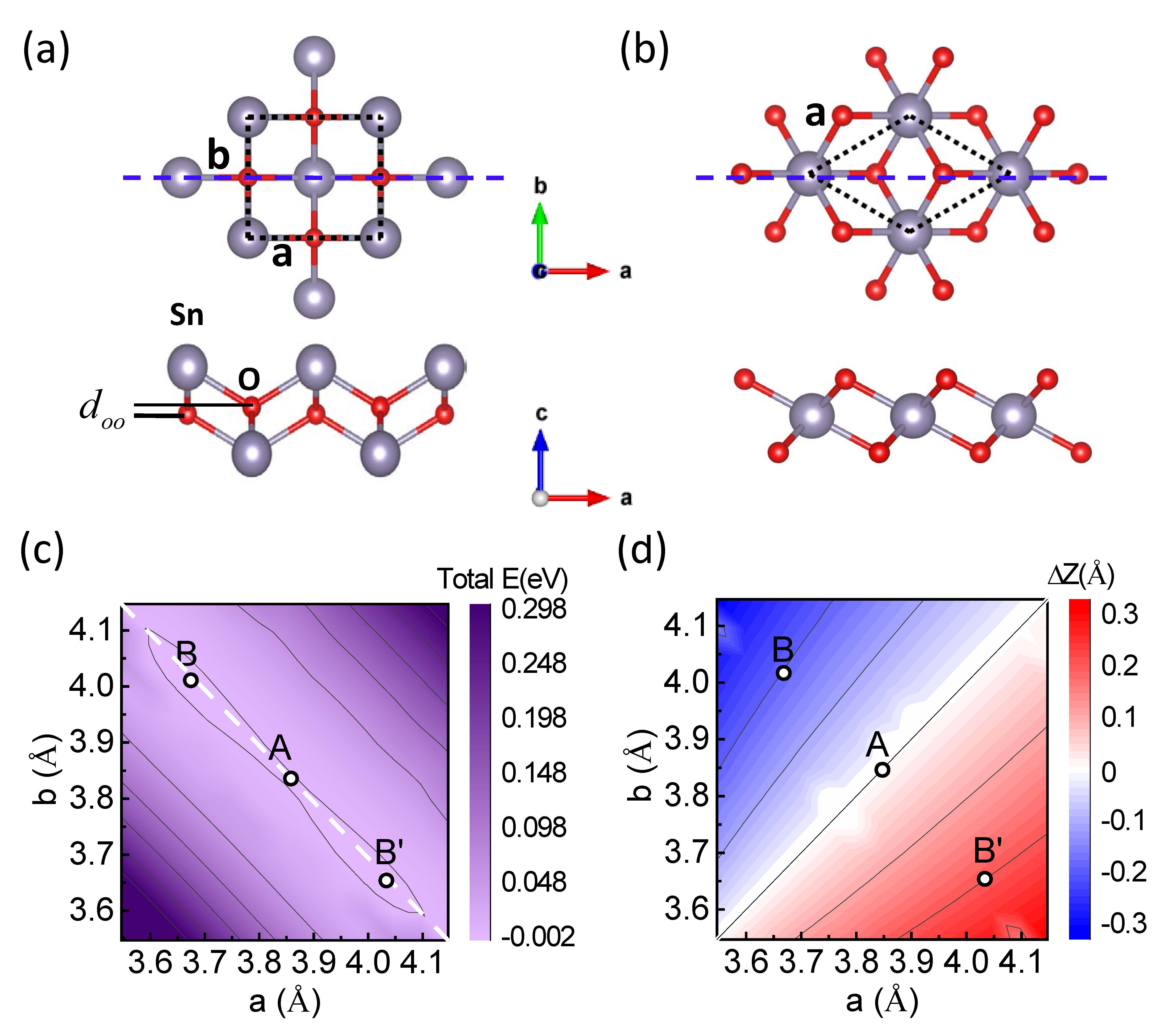
Figure 1(a) displays the lattice crystal of monolayer SnO, with two Sn and O atoms in a unit cell. and is the lattice constant along - and -axis, respectively. Unlike bulk and bilayer SnO, monolayer SnO with Å (labeled as phase A) is unstable (see Fig. S2(a-c) in the supplementary material), agreeing with previous works. Zhou and Umezawa (2015); Mounet et al. (2018) The eigenvectors of phonon modes with imaginary frequencies correspond to the anti-directional movement of O atoms along the -axis. The contour of total energy of monolayer SnO, as the function of and , is presented in Fig. 1(c). Compared to phase A, another rectangle structure is more stable which has Å and Å, or vice versa (labeled as phase B or B). For more clarity, Fig. S2(d) in the supplementary material displays the energy profile along the path B-A-B (see bash line in Fig. 1(c)). Meanwhile, the distance between O atoms () along the direction changes from zero in phase A to 0.2 Å in phase B (see Fig. 1(d)). That is consistent with aforementioned eigen-displacement of the imaginary modes in phase A. Moreover, the structural instability of phase A was further identified with different simulation methods (see Fig. S2(d) in the supplementary material). For the case of monolayer SnO2, we adopted T-phase structure Xiao, Xiao, and Wang (2016) (see Fig. 1(b)). The thickness of monolayer SnO2 is chosen by the interlayer distance of bilayer SnO2 with the most stable structure (see Fig. S3 in the supplementary material). All the optimized structural parameters are listed in Table. 1. The crystal symmetry of crystal lattice of monolayer SnO is while that of monolayer SnO2 is which contains an inversion center on Sn site. The bonding length of Sn-O is longer in monolayer SnO than that in monolayer SnO2.
| (Å) | (Å) | (Å) | |
|---|---|---|---|
| SnO | 4.022,3.663 | 2.281, 2.228 | 4.826 |
| SnO2 | 3.227 | 2.121 | 4.272 |
Pristine 2D tin oxides are non-magnetic semiconductors (see Fig. S4 in the supplementary material) and heat is mainly carried by phonons. The phonon dispersions of monolayer SnO in phase B and monolayer SnO2 are displayed in Fig. 2(a,b), which ensure their structural stability. The lowest three branches are the out-of-plane acoustic (ZA), transverse acoustic (TA) and longitudinal acoustic (LA) branch. ZA branch has a quadratic dispersion near the point. Carrete et al. (2016) An acoustic-optical gap is absent and present in the phonon dispersion of monolayer SnO and SnO2, respectively. The low- and high-frequency phonon modes are mainly dominated by the vibration of Sn and O atoms, respectively (see Fig. S5 in the supplementary material).
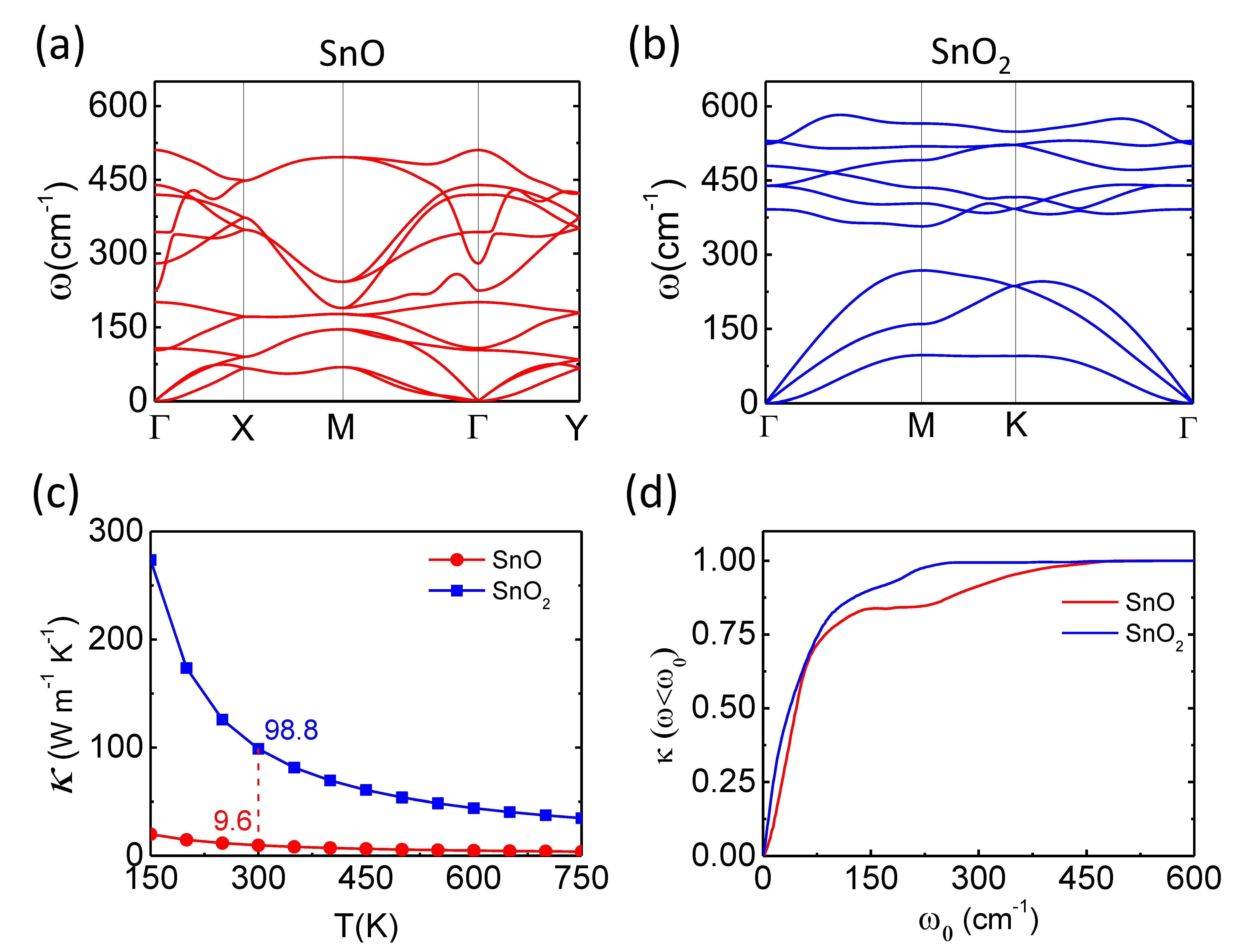
The temperatures (T) dependence of without boundary scattering is shown in Fig. 2(c). At room temperature, the of monolayer SnO2 reaches 98.8 W/(mK), comparable with that of conventional semiconducting Ge (65 W/(mK)) Morelli and A. (2006) and GaAs (45 W/(mK)). Morelli and A. (2006) Though the lattice crystal of monolayer SnO is anisotropic, its is almost isotopic. The small anisotropy of is keeping pace with that of phonon group velocity, Qin et al. (2016) which can be further attributed to the similar atomic bonding characteristics along the - and -direction (see Fig. S6 in the supplementary material). It is possible to induce the anisotropic thermal transport into 2D tin oxides by dislocation Sun et al. (2018) or uniaxial strain Fan et al. (2017) for broadening their potential applications in future. We will only discuss the along the -axis hereafter. The room-temperature of monolayer SnO, however, is only 9.6 W/(mK) which is ten times smaller than that of SnO2. Such a large imparity of is consistent with the large difference between the of bulk SnO and SnO2 observed in experiment. Kuwahara et al. (2018) Therefore, thermal transport is the limit factor in electronic applications of 2D SnO rather than 2D SnO2.
By fitting the phonon density of states (DOS) at low phonon frequencies with a Debye model, Togo and Tanaka (2015) we obtained Debye temperature as 259 K and 356 K for monolayer SnO and SnO2, respectively. As a result, the dependence of of monolayer SnO2 follows the relation of at temperature lower than . Ziman (1960) Here is an empirical parameter which was fitted as 1.02 (see Fig. S7(d) in the supplementary material). At temperature substantially beyond , the overall dependence of of 2D tin oxides restores the behavior (see Fig. S7 in the supplementary material).
We found that the effect of isotopic impurities scattering to is small compared with the anharmonic scattering in the temperature above 250 K. For example, if we exclude the from the total in Eq. 2, the room-temperature will increase only by 0.6% and 3.3% for monolayer SnO and SnO2, respectively. The is inversely proportional to atomic mass Li et al. (2014) which is not very small for tin oxides.
The normalized cumulative , which represents the contribution of from the phonons with frequencies less than , is shown in Fig. 2(d). In the case of monolayer SnO, apart from the acoustic phonons, optical phonons with frequency up to 470 cm-1 have a non-negligible contribution ( 20%) to (see Fig. 2(d) and Fig. S8(a) in the supplementary material). That can be attributed to the high dispersive relation and large group velocity of optical phonons (see Fig. 2(a) and Fig. 4(a)). In contrast, the of monolayer SnO2 is dominated by acoustic phonons with frequency less than 250 cm-1 (see Fig. 2(d)).
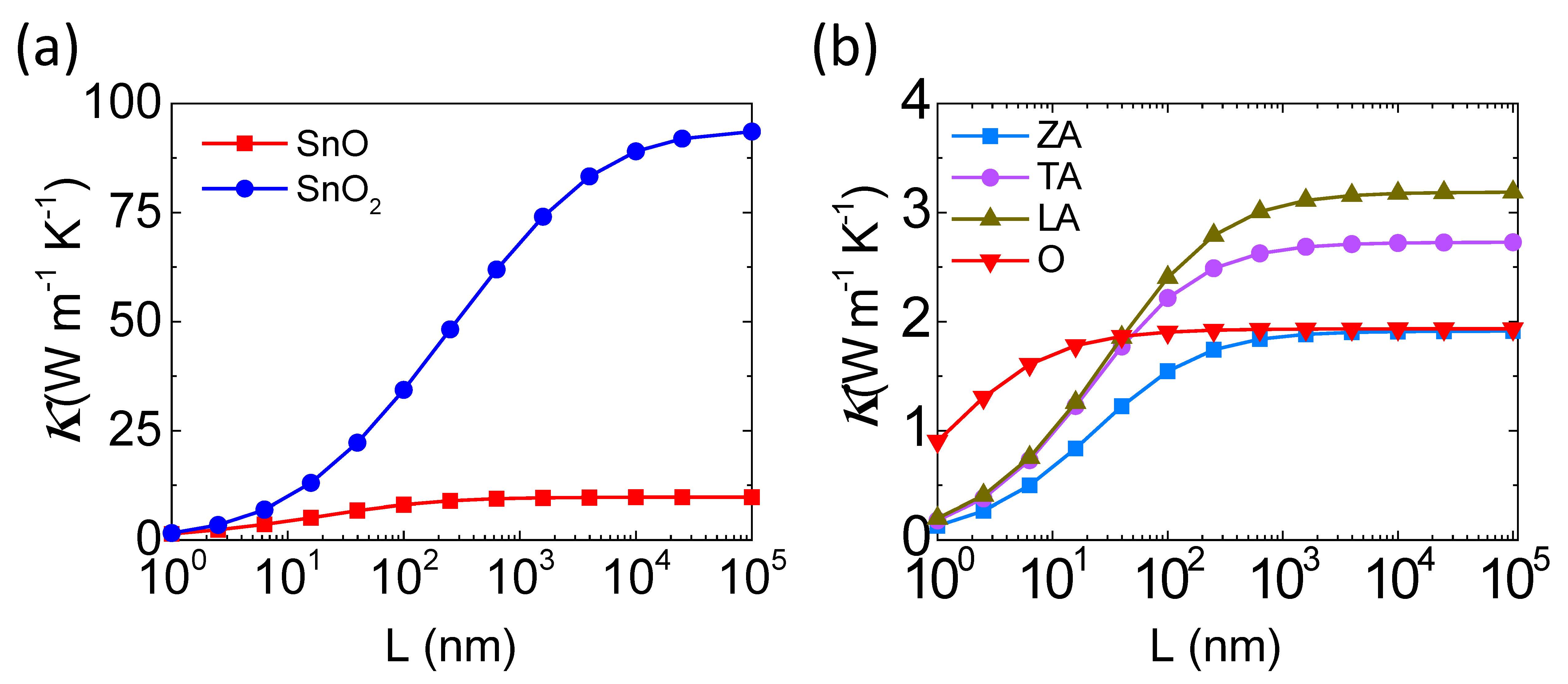
The phonon scattering from rough edge can decrease the of semiconductors to achieve excellent thermoelectricity. Hochbaum et al. (2008) Here the size effect of is discussed in the range of diffusive thermal transport. The lateral size () dependence of room-temperature and the contribution of phonons from different branches are displayed in Fig. 3. At room temperature, the mean free path (MFP) of phonon is about and nm for monolayer SnO and SnO2, respectively. In the case of monolayer SnO, though the contribution of from acoustic phonons can be decreased by enhanced boundary scattering, the contribution from optical phonons is almost size independent until the decreases down to 10 nm (see Fig. 3(b)), due to its small MFP. Thus, as the lateral size of 2D SnO decreases from nm, nanostructuring might not be an efficient method to reduce its , due to the coexistence of size dependent and independent component. In contrast, the of 2D SnO2, which is dominated by acoustic phonons, can be effectively decreased by edge roughness scattering (see Fig. 3(a)).
The large difference between the of monolayer SnO and SnO2 can not be simply attributed to the different mean atomic mass. We analyzed the role of each term in Eq. 1 in determining the of 2D tin oxides. Figure 4(a) displays the frequency dependence of mode group velocity . The of low-frequency phonon modes ( cm-1) in monolayer SnO2 is higher than that in monolayer SnO. The group velocity of phonon is large for materials with light atomic mass and strong bonding. The bond strength can be reflected by the 2D elastic module , which can be obtained through a fitting process of total energy with respect to strain. Qiao et al. (2014) The of monolayer SnO along - and -axis is 40.96 J/m2 and 34.98 J/m2, much smaller than J/m2 of monolayer SnO2 (see Fig. S9 in the supplementary material). The weak Sn-O bonding results in small phonon group velocity as well as aforementioned long Sn-O bond length in monolayer SnO (see Table. 1).
The mode phonon lifetimes of 2D tin oxides at room temperature are shown in Fig. 4(b). It can be seen that the overall of monolayer SnO2 is larger than that of monolayer SnO. As mentioned above, anharmonic effect dominates the phonon scattering in the thermal transport of 2D tin oxides. The scattering rate depends on both the square of Grüneisen parameter and the available three-phonon phase space (P3)q,s. Ziman (1960) The former one describes the strength of anharmonicity. The latter one represents the number of anharmonic scattering channel for phonon absorption processes and emission processes, according to the energy and momentum conservations. Li et al. (2014)
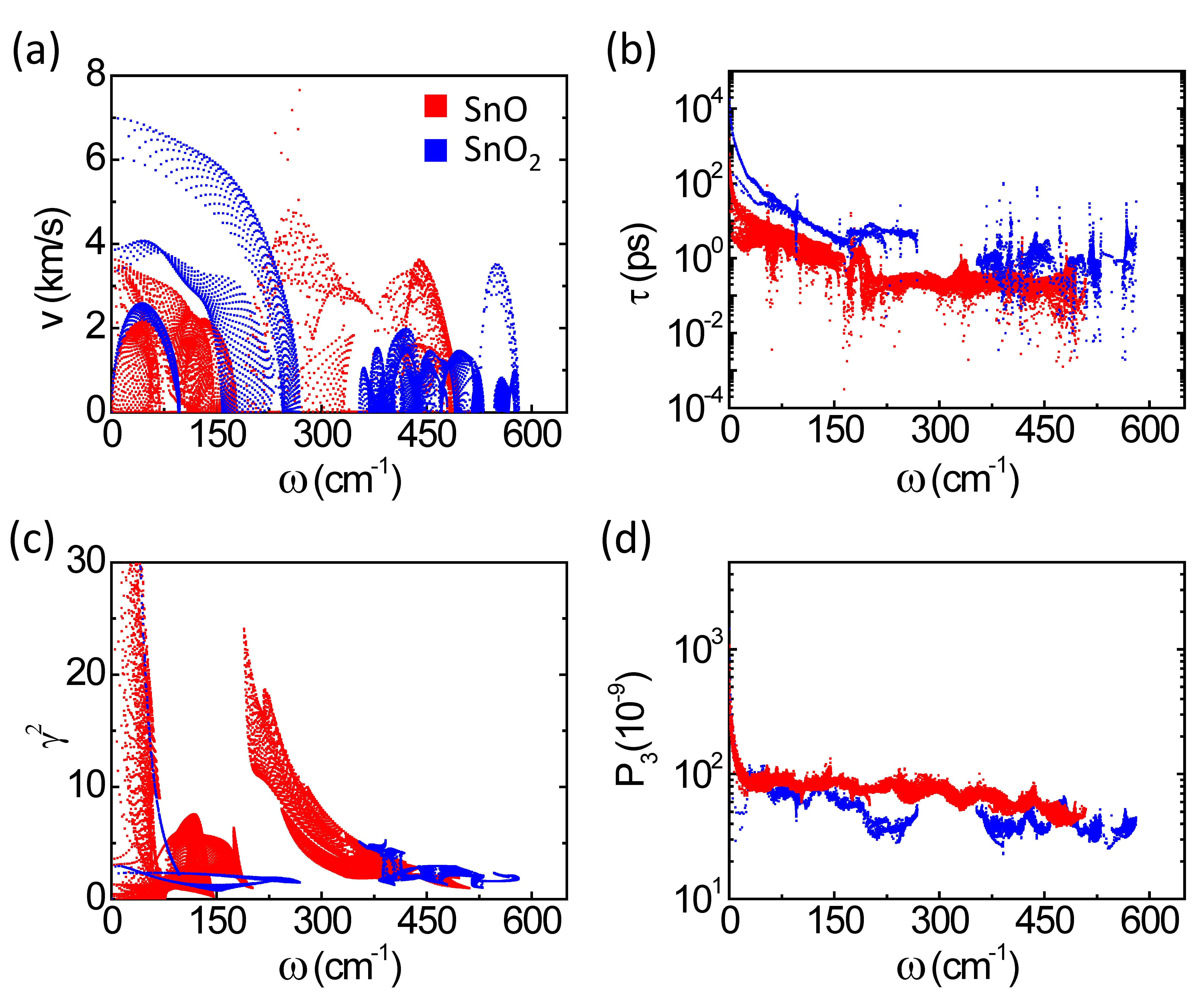
The overall of monolayer SnO is much larger than that of monolayer SnO2, which can be seen from Fig. 4(c). That is also consistent with the fact that the acoustic phonon branches of monolayer SnO are significantly softened compared to that of monolayer SnO2 (see Fig. 2). The overall of monolayer SnO is slightly larger than that of SnO2 (see Fig. 4(d)). In the phonon dispersion of monolayer SnO, the soft acoustic phonons and intersection between acoustic and optical branches (see Fig. 2(a)) provide more channels for anharmonic scattering, especially for emission process of high-frequency phonons (see Fig. S10 in the supplementary material). Combining with Fig. 4(c) and 4(d), the small in monolayer SnO is mainly due to the large . Thus, the much small of monolayer SnO arises from the small phonon group velocity and strong anharmonicity strength.
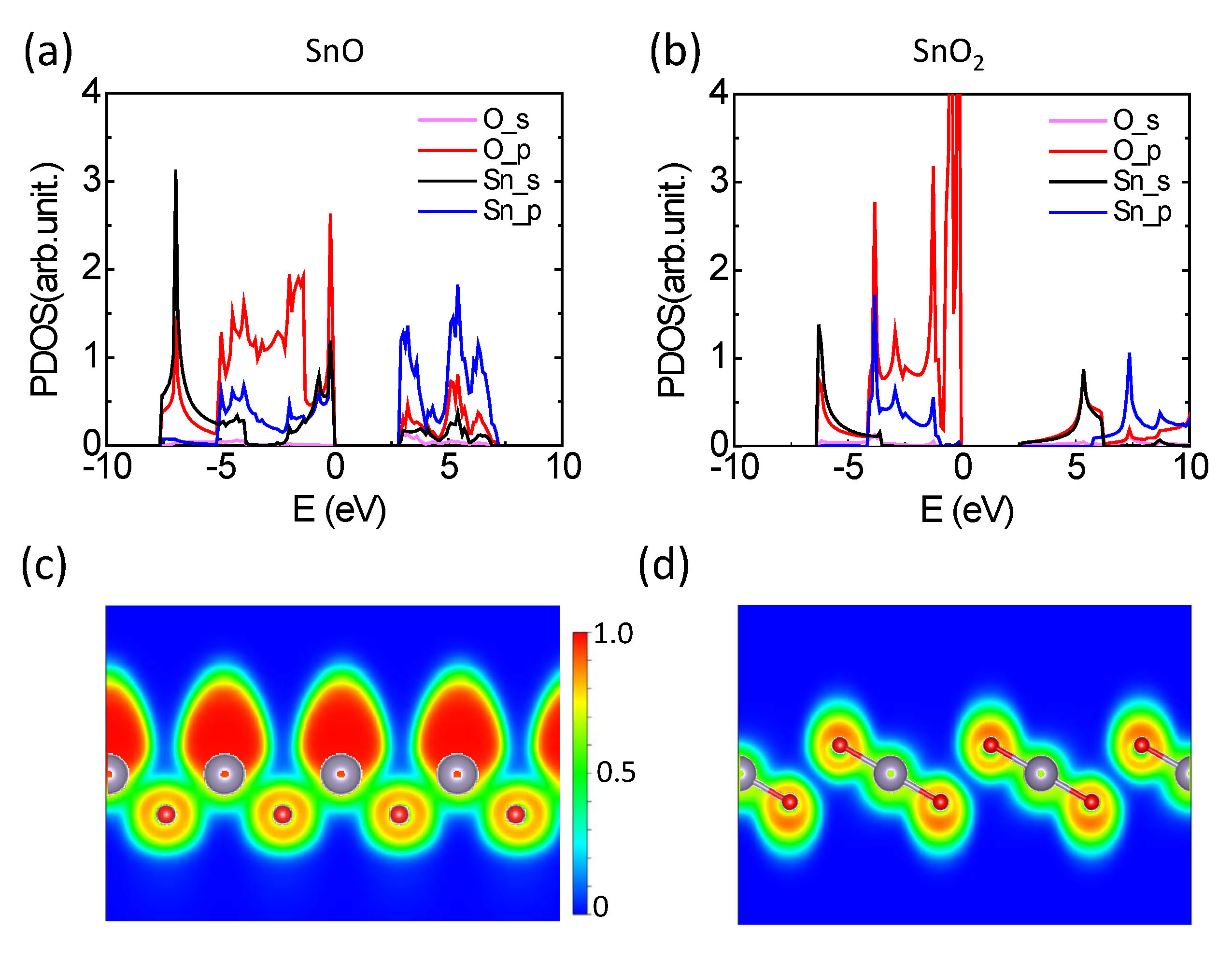
The large imparity between the anharmonicity strength of tin oxides can be further attributed to the electron configuration. The projected density of states (PDOS) of tin oxides are shown in Fig. 5(a) and 5(b). In the valence band of monolayer SnO, Sn-5 electrons interact with the O-2 states, with the bonding states locating between -8 and -5 eV and anti-bonding states appears at upper valence bands (see Fig. 5(a) and Fig. S11 in the supplementary material). The anti-bonding states, with a large contribution from the Sn-5 states, can hybridize with Sn-5 states due to the lack of inversion symmetry. This sort of hybridization shifts the energy of anti-bonding states downward, thereby stabilizing it at the top of valence bands.Watson and Parker (1999) The filled anti-bonding states result in the sterically active lone-pair electrons (see Fig. S11 in the supplementary material), similar to the case of bulk SnO. Watson (2001) The electronic local function (ELF) was calculated with the location of cross-section indicated by the blue line in Fig. 1(a, b), which can directly give a picture of lone-pair electrons. The ELF shows a strong electron localization around the Sn atom (see Fig. 5(c)), consistent with the distribution of lone pair at Sn. As a result, the overlapping wave functions of the lone-pair electrons and nearby O-2 bonding electrons will induce a nonlinear repulsive electrostatic force during thermal agitation, Skoug and Morelli (2011); Qin et al. (2018) leading to enhanced anharmonicity and small phonon lifetime. Additionally, it is indicated that chemical functionalization can effectively modulate the of 2D SnO since the lone-pair electrons distribute on the surface.
In contrast to SnO, the lattice crystal of monolayer SnO2 is centrosymmetric. The mixing between Sn- states and anti-bonding states of O- and Sn- is prohibited due to the different parity of and orbital. The anti-bonding states of O- and Sn- is above the Fermi level and unfilled. Thus, both the and electrons of Sn atom participate in Sn-O bonding in a form of hybridization. Electrons transfer from Sn to O atom, as shown in Fig. 5(d) and Fig. S11. The absence of lone-pair electrons make anharmonicity strength to be smaller for monolayer SnO2 than for monolayer SnO (see Fig. 4(c)), resulting in longer phonon life time (see Fig. 4(b)).
In conclusion, based on the first-principles calculations, we calculated the thermal conductivity of monolayer SnO and SnO2. The tetragonal lattice of monolayer SnO spontaneously transforms to a rectangle one. The room-temperature of monolayer SnO and SnO2 arrives at 9.6 W/(mK) and 98.8 W/(mK), respectively. The size effect of is much weaker for monolayer SnO than for monolayer SnO2, due to the coexistence of size-dependent and size-independent contribution of in monolayer SnO. The small of monolayer SnO is due to the small phonon group velocity and strong anharmonicity strength. That can be further attributed to the existence of sterically active lone-pair electrons distributed on the surface of monolayer SnO. This work may give a guide for the thermal management in the electronic or thermoelectrical devices based on 2D tin oxides.
Supplementary Material
See supplementary material for the computational details; The convergence test of ; The phonon dispersion of monolayer, bilayer and bulk SnO with a = b; The structural and energetical properties of bilayer SnO2; The 2D effective elastic module, band structure, projected phonon density of states of monolayer SnO and SnO2; The isotropic of monolayer SnO; The temperature dependence of of monolayer SnO and SnO2; The contribution of from different branches; The three-phonon scattering phase space for absorption and emission process; The distribution of charge density of monolayer SnO and SnO2.
Acknowledgements.
This work was supported by the NSFC (Grants No.11747054), the Specialized Research Fund for the Doctoral Program of Higher Education of China (Grant No.2018M631760), the Project of Heibei Educational Department, China (No. ZD2018015 and QN2018012), and the Advanced Postdoctoral Programs of Hebei Province (No.B2017003004).References
- Novoselov et al. (2005) K. S. Novoselov, A. K. Geim, S. V. Morozov, D. Jiang, M. I. Katsnelson, I. V. Grigorieva, S. V. Dubonos, and A. A. Firsov, Nature 438, 197 (2005).
- Chhowalla et al. (2013) M. Chhowalla, H. S. Shin, G. Eda, L.-J. Li, K. P. Loh, and H. Zhang, Nat. Chem. 5, 263 (2013).
- Nicolosi et al. (2013) V. Nicolosi, M. Chhowalla, M. G. Kanatzidis, M. S. Strano, and J. N. Coleman, Science 340, 1226419 (2013).
- Ziletti et al. (2015) A. Ziletti, A. Carvalho, D. K. Campbell, D. F. Coker, and A. H. Castro Neto, Phys. Rev. Lett. 114, 046801 (2015).
- Cui et al. (2015) S. Cui, Z. Wen, X. Huang, J. Chang, and J. Chen, Small 11, 2305–2313 (2015).
- Daeneke et al. (2017) T. Daeneke, P. Atkin, R. Orrell-Trigg, A. Zavabeti, T. Ahmed, S. Walia, M. Liu, Y. Tachibana, M. Javaid, A. D. Greentree, S. P. Russo, R. B. Kaner, and K. Kalantar-Zadeh, ACS Nano 11, 10974–10983 (2017).
- Sui and Charpentier (2012) R. Sui and P. Charpentier, Chem. Rev. 112, 3057–3082 (2012).
- Tokura and Nagaosa (2000) Y. Tokura and N. Nagaosa, Science 288, 462–468 (2000).
- Miller et al. (2017) S. A. Miller, P. Gorai, U. Aydemir, T. O. Mason, V. Stevanović, E. S. Toberer, and G. J. Snyder, J. Mater. Chem. C 5, 8854–8861 (2017).
- Padova et al. (1994) P. D. Padova, M. Fanfoni, R. Larciprete, M. Mangiantini, S. Priori, and P. Perfetti, Surf. Sci. 313, 379 – 391 (1994).
- Lee et al. (2018) J.-H. Lee, M. Yoo, D. Kang, H.-M. Lee, W.-h. Choi, J. W. Park, Y. Yi, H. Y. Kim, and J.-S. Park, ACS Appl. Mater. Interfaces 10, 33335–33342 (2018).
- Hien et al. (2014) V. X. Hien, J.-H. Lee, J.-J. Kim, and Y.-W. Heo, Sens. Actuators, B 194, 134 – 141 (2014).
- Kumar et al. (2009) V. Kumar, S. Sen, K. Muthe, N. Gaur, S. Gupta, and J. Yakhmi, Sens. Actuators, B 138, 587 – 590 (2009).
- Qiang et al. (2017) L. Qiang, W. Liu, Y. Pei, G. Wang, and R. Yao, Solid-State Electron. 129, 163 – 167 (2017).
- Dattoli et al. (2007) E. N. Dattoli, Q. Wan, W. Guo, Y. Chen, X. Pan, and W. Lu, Nano Lett. 7, 2463–2469 (2007).
- Zhang et al. (2017) F. Zhang, J. Zhu, D. Zhang, U. Schwingenschlögl, and H. N. Alshareef, Nano Lett. 17, 1302–1311 (2017).
- Yuan et al. (2006) L. Yuan, Z. Guo, K. Konstantinov, H. Liu, and S. Dou, J. Power Sources 159, 345 – 348 (2006).
- Tsai et al. (2011) F.-S. Tsai, S.-J. Wang, Y.-C. Tu, Y.-W. Hsu, C.-Y. Kuo, Z.-S. Lin, and R.-M. Ko, Appl. Phys Express 4, 025002 (2011).
- Nomura, Kamiya, and Hosono (2011) K. Nomura, T. Kamiya, and H. Hosono, Adv. Mater. 23, 3431–3434 (2011).
- Ogale et al. (2003) S. B. Ogale, R. J. Choudhary, J. P. Buban, S. E. Lofland, S. R. Shinde, S. N. Kale, V. N. Kulkarni, J. Higgins, C. Lanci, J. R. Simpson, N. D. Browning, S. Das Sarma, H. D. Drew, R. L. Greene, and T. Venkatesan, Phys. Rev. Lett. 91, 077205 (2003).
- Singh et al. (2017) M. Singh, E. D. Gaspera, T. Ahmed, S. Walia, R. Ramanathan, J. van Embden, E. Mayes, and V. Bansal, 2D Materials 4, 025110 (2017).
- Saji et al. (2016) K. J. Saji, K. Tian, M. Snure, and A. Tiwari, Adv. Electron. Mater. 2, 1500453 (2016).
- Seixas et al. (2016) L. Seixas, A. S. Rodin, A. Carvalho, and A. H. Castro Neto, Phys. Rev. Lett. 116, 206803 (2016).
- Chen et al. (2012) H. Chen, L. Hu, X. Fang, and L. Wu, Adv. Funct. Mater. 22, 1229–1235 (2012).
- Xiao, Xiao, and Wang (2016) W.-Z. Xiao, G. Xiao, and L.-L. Wang, J. Chem. Phys. 145, 174702 (2016).
- Luan et al. (2014) H.-X. Luan, C.-W. Zhang, F. Li, P. Li, M.-J. Ren, M. Yuan, W.-X. Ji, and P.-J. Wang, RSC Adv. 4, 9602–9607 (2014).
- Feng et al. (2015) Y. Feng, W.-X. Ji, B.-J. Huang, X.-l. Chen, F. Li, P. Li, C.-w. Zhang, and P.-J. Wang, RSC Adv. 5, 24306–24312 (2015).
- Zou and Balandin (2001) J. Zou and A. Balandin, J. Appl. Phys. 89, 2932–2938 (2001).
- Hochbaum et al. (2008) A. I. Hochbaum, R. Chen, R. D. Delgado, W. Liang, E. C. Garnett, M. Najarian, A. Majumdar, and P. Yang, Nature 451, 163–167 (2008).
- Li et al. (2014) W. Li, J. Carrete, N. A. Katcho, and N. Mingo, Comput. Phys. Commun. 185, 1747 – 1758 (2014).
- Zhou and Umezawa (2015) W. Zhou and N. Umezawa, Phys. Chem. Chem. Phys. 17, 17816–17820 (2015).
- Mounet et al. (2018) N. Mounet, M. Gibertini, P. Schwaller, D. Campi, A. Merkys, A. Marrazzo, T. Sohier, I. E. Castelli, A. Cepellotti, G. Pizzi, and N. Marzari, Nat. Nanotechnol. 13, 246–252 (2018).
- Carrete et al. (2016) J. Carrete, W. Li, L. Lindsay, D. A. Broido, L. J. Gallego, and N. Mingo, Mater. Res. Lett. 4, 204–211 (2016).
- Morelli and A. (2006) D. T. Morelli and S. G. A., edited by S. L. Shindé and J. Goela (Springer-Verlag New York, 2006).
- Qin et al. (2016) G. Qin, Z. Qin, W.-Z. Fang, L.-C. Zhang, S.-Y. Yue, Q.-B. Yan, M. Hu, and G. Su, Nanoscale 8, 11306–11319 (2016).
- Sun et al. (2018) B. Sun, G. Haunschild, C. Polanco, J. Z.-J. Ju, L. Lindsay, G. KoblmMei ller, and Y. K. Koh, Nat. Mater. (2018), 10.1038/s41563-018-0250-y.
- Fan et al. (2017) D. Fan, H. Sigg, R. Spolenak, and Y. Ekinci, Phys. Rev. B 96, 115307 (2017).
- Kuwahara et al. (2018) S. Kuwahara, S. at Tanusilp, Y. Ohishi, H. Muta, S. Yamanaka, and K. Kurosaki, Mater. Trans. 59, 1022–1029 (2018).
- Togo and Tanaka (2015) A. Togo and I. Tanaka, Scripta Mater. 108, 1 – 5 (2015).
- Ziman (1960) J. M. Ziman, International series of monographs on physics (Clarendon Press, Oxford, 1960).
- Qiao et al. (2014) J. Qiao, X. Kong, Z.-X. Hu, F. Yang, and W. Ji, Nat. Commun. 5, 4475 (2014).
- Watson and Parker (1999) G. W. Watson and S. C. Parker, J. Phys. Chem. B 103, 1258–1262 (1999).
- Watson (2001) G. W. Watson, J. Chem. Phys. 114, 758–763 (2001).
- Skoug and Morelli (2011) E. J. Skoug and D. T. Morelli, Phys. Rev. Lett. 107, 235901 (2011).
- Qin et al. (2018) G. Qin, Z. Qin, H. Wang, and M. Hu, Nano Energy 50, 425 – 430 (2018).