Highly confined Love waves modes by defect states
in a holey SiO2/quartz phononic crystal111Accepted for publication in Journal of Applied Physics
Abstract
Highly confined Love modes are demonstrated in a phononic crystal based on a square array of etched holes in SiO2 deposited on the ST-cut quartz. An optimal choice of the geometrical parameters contributes to a wide stop-band for shear waves’ modes. The introduction of a defect by removing lines of holes leads to the nearly flat modes within the band gap and consequently paves the way to implement advanced designs of electroacoustic filters and high-performance cavity resonators. The calculations are based on the finite element method in considering the elastic and piezoelectric properties of the materials. Interdigital transducers are employed to measure the transmission spectra. The geometrical parameters enabling the appearance of confined cavity modes within the band gap and the efficiency of the electric excitation were investigated.
pacs:
68.60.BsI INTRODUCTION
Phononic crystals (PnCs), as an elastic analog of the photonic crystals, have received increasing attention in the last two decades. PnCs are widely investigated for their potential applications in various areas, including RF communications[1; 2; 3; 4; 5; 6; 7], acoustic isolators[8; 9; 10; 11; 12; 13], sensors[14; 15; 16; 17; 18; 19], thermoelectric materials[20; 21; 22; 23] and meta-materials[24; 25; 26; 27; 28; 29; 30; 31; 32]. Composed of 1D, 2D, or 3D periodic arrays of inclusions embedded in a matrix, PnCs give rise to the complete or partial band gaps for both bulk acoustic waves (BAW)[33; 34; 35; 36; 1; 5] and surface acoustic waves (SAW)[37; 38; 39; 9; 40; 41; 42; 12; 43; 44]. The introduction of defects into PnCs is at the origin of multiple applications such as waveguide[45; 2; 46], cavity[1; 47; 48], filter[49; 5] and multiplexer[50]. Most research on the defect modes is based on the bulk waves[1; 2; 5], Rayleigh waves[51] and Lamb waves[52; 47], while sensors, especially the bio-sensors, are based on the Love waves and antisymmetric Lamb waves, which are compatible with the liquid environment[15; 16] and leak less energy in the liquid. However, Lamb waves propagate on the extremely thin slabs, making them comparably fragile and therefore difficult to manipulate. Whereas Love waves, a shear horizontal (SH) polarized SAW, exist in the guiding layer deposited on a semi-infinite substrate, which guarantees both the confinement of the energy and the toughness of the device, in comparison with the Lamb waves devices. In recent years, the partial band-gap effect of PnCs on Love waves has been reported and a reflective grating was then proposed[43; 12]. Nevertheless, the exploitation of Love waves interacting with the defect states in PnCs remains to be investigated.
In this paper, we demonstrate the acoustic band gap effect in a 2D PnC consisting of a square array of holes in a thin amorphous SiO2 (silica) layer covering a ST-cut quartz substrate. Localized defect or cavity modes in the band gap which are introduced by removing lines of holes in the lattice are observed. The efficiency of cavity modes in the isolation of PnC is investigated as a function of the geometrical parameters of PnC and cavity. These effects are used to design micro-electromechanical resonators with highly confined cavity modes of Love waves. The band structures and transmission spectra are calculated with the finite element method (FEM, COMSOL Multiphysics®). The transmission spectra are compared with the dispersion curves and the resonant frequencies, showing good compatibility.
II Models and Simulation
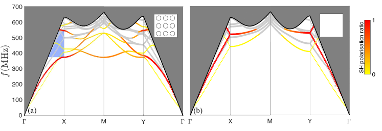
The guiding layer of Love waves is silica (kg/m3,), with a height of , covering a -height 90ST-cut quartz substrate (Euler angles=(0°, 47.25°, 90°), LH 1978 IEEE), which has been rotated 90 degrees around the -axis from the ST-cut quartz, for a fast SH waves (5000m/s) can be generated by the electric field. The shear wave velocity in the silica film is 3438m/s, less than that in the 90ST-cut quartz substrate, indicating the existence of Love waves. The cylindrical holes in the silica film have a radius of . The square array period or the lattice constant is . The air hole is chosen because of its strong contrast in density and elastic constants with regard to the silica. A unit cell of the PnC constructed in COMSOL, showing in Fig 1(a), is employed to calculate the dispersion curves or the band structure. Floquet periodic boundary conditions are applied along the x and y directions to form a whole crystal, and the bottom of the substrate is assumed fixed. Love waves propagate along the -axis (the -axis of the ST-cut quartz), where Rayleigh waves can not be generated[12] due to a zero electromechanical coupling factor to the substrate. The first Brillouin zone (BZ) of the PnC is shown in Fig 1(b). Considering the anisotropy of the quartz substrate, the irreducible BZ is a square bounded by -X-M-Y-. The surface of the PnC coincides with the plane . The wavelength normalized energy depth (NED) is calculated to select the surface modes for which is less than 1.
| (1) |
is the stress and the strain. The asterisk (*) signifies the complex conjugate. denotes the whole domain of the unit cell. is the wavelength. Note that the integral in the denominator is the total acoustic potential energy in the unit cell and that the integral in the numerator is weighted by the depth of the point where the acoustic energy is not zero. That means if the average depth of the energy is less than the wavelength, the NED will be less than 1. The NED can well select the modes with speed less than the SH wave velocity of the substrate, where the wave vector is relatively large. As for a relatively small , is fixed to that is resulting from and . Moreover, the NED can filter out the plate modes appeared in our finite-depth substrate which is supposed to be semi-infinite for Love waves.
Surface modes include SH type SAW and Rayleigh type SAW. The ratio of SH polarization is calculated to distinguish between Love waves and Rayleigh waves.
| (2) |
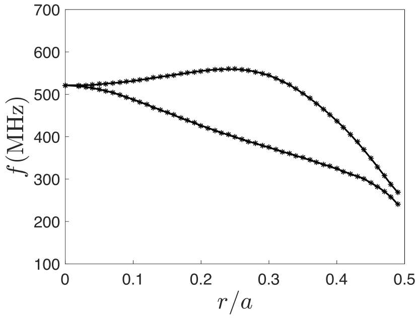
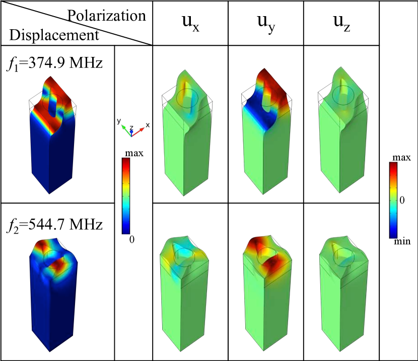
and are respectively the displacements along the directions. is the SH displacement component that can be expressed as , which is perpendicular to the wave vector . is the angle between and the -axis with . The complete band structure calculated with COMSOL is shown in Fig 2(a). The gray part is the radiation zone, where the waves diffuse to the volume (the bulk waves). The black line is the dispersion relation of the SH waves (here the fast shear waves) in the substrate, according to . The curves in red and yellow denote the surface polarization modes. With the change of propagation direction, certain modes become gray as they start to diffuse into the volume. The modes colors are determined by their SH ratio. The red modes have a large SH ratio, indicating the Love modes. The yellower the modes, the closer they are to the Rayleigh type. Orange implies a coupling between Love modes and Rayleigh modes. In the -X direction, the Love waves are not coupled to the Rayleigh waves, showing a large band gap ranging from 374.9 to 544.7 MHz between the two Love modes. Band structure without PnC is shown in Fig 2(b), with no band gap for the Love modes. The relation between the band gap width and the normalized hole radius is shown by the two black curves in Fig 3, where the band gap is between the two curves representing the two Love modes, consistent with the results reported by LIU et al.[43]. The PnC gives rise to the appearance of the band gap, and the band width reaches a maximum (170.3 MHz) at =0.29. Since the center of the band gap tends to decrease with the augmentation of the normalized radius, the relative band width () reaches its maximum (37.1%) at =0.31. The displacement fields of the two Love modes at the point X of the BZ and their polarizations along the three axis are shown in Fig 4. It is found that the polarizations along the -axis and the -axis are negligible compared with the polarization on the -axis, which means the polarizations of the two modes are horizontally perpendicular to the wave propagation direction (-axis), proving that they are of SH type. Due to the exclusive generation of Love waves by the generated electric field, we only consider the Love modes in the rest of this paper. As the wave vector deviates from the -axis, the band gap closes in the center of X-M. Therefore the propagation direction for calculating the transmission is along the -axis.
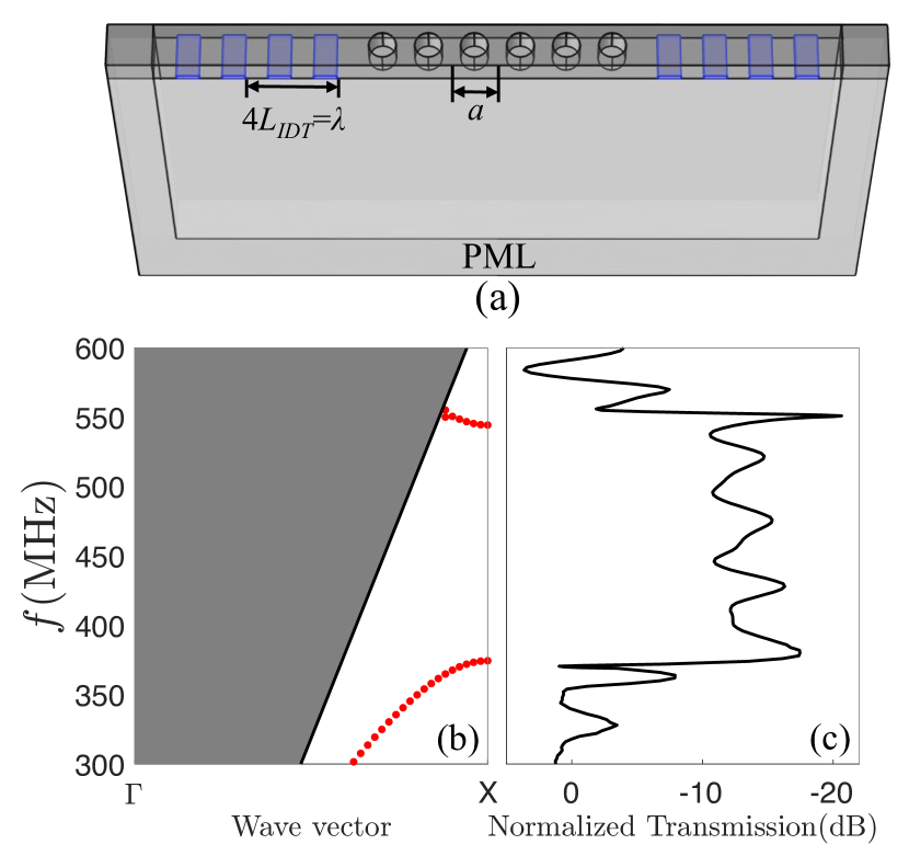
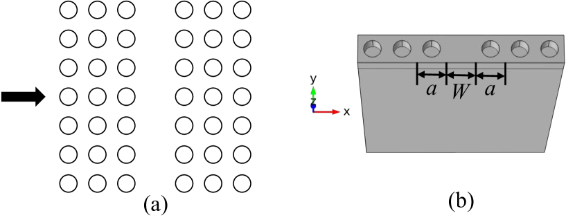
The calculation of transmission spectra is realized by simulating a SAW device consisting of two parts of aluminum inter-digital transducers (IDTs) and a PnC located between the IDTs. The height of IDTs is . The IDTs are constructed on the quartz surface which is piezoelectric to generate the electric field. The graphic representation of the model is shown in Fig 5(a). Since the device has translational symmetry along the -axis which is perpendicular to the direction of propagation, periodic boundary conditions are applied along the -axis, reducing the simulation structure to only one period. The model is surrounded by perfectly matched layers (PMLs) for absorbing the undesired reflections from the boundary. The bottom and lateral sides are assumed fixed. One of the IDTs performing as a transmitter is given a harmonic voltage signal, with an amplitude of 1, to excite acoustic waves in the quartz substrate. These waves are confined in the silica film and propagate through the PnC. They are received by the IDT on the other side. The output is measured by averaging the voltage difference between the odd and even fingers. The odd fingers of the input and output IDTs are assigned to the electrical ground. The even fingers of the output IDT are set to zero surface charge accumulation. Note that the width of the IDT fingers should be updated for each frequency in the spectrum according to the relation . is the velocity of Love waves for , resulting from the basic dispersion relation of Love waves. That is, each frequency corresponds to a single wave velocity and wavelength. This frequency response is then normalized by that of the matrix (without PnC) to show the transmission loss contributed by the PnC only. Our previous work[53] has proved the reliability of this model, giving coincident results between simulations and experiments. Fig 5(c) shows the normalized transmission spectra of the PnC, calculated with 10 PnC holes in center and 20 IDT fingers on each side. The attenuation appears clear and is consistent with the band structure prediction.
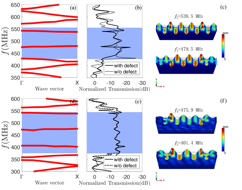
The resonator is realized by removing lines of holes along the direction in the PnC lattice, forming a cavity perpendicular to the propagation direction. A supercell containing 1×() unit cells is constructed and shown in Fig 6(b), with periodic boundary conditions applied in the and directions. Here we set the cavity width to . The band structures of Love waves in the PnCs containing the defect are calculated along -X and are shown in Fig 7(a) and (d), for =0.2 and 0.3 respectively. Note that the -X is 11 times smaller as we calculate for a supercell which is 11 times longer, and the band structure will be folded and repeated 11 times in the rest part. It is found that new flat modes, referred to as defect modes or cavity modes, appear inside the previously observed band gaps. These band structures are attributed to the coupling between the cavity and the perfect PnCs. Two cavity modes are predicted in Fig 7(a), respectively at 479.5 MHz and 538.5 MHz. In Fig 7(d), another two are at 401.4 and 475.9 MHz. The corresponding displacement fields of the cavity modes are shown in Fig 7(c) and (f). The displacements are concentrated in the center of the model (in the cavity) and attenuated at both ends. Inside the cavity, the displacements are uniform throughout the defect with maximums near the edges. It can be seen that the cavity modes for are more confined to the surface than that for the radius of . In Fig 7(d), the flat mode on the upper limit of the band-gap region is not referred to as a cavity mode, since its displacement is no more concentrated in the cavity. Fig 7(b) and (e) show the normalized transmission spectra with and without the cavity in the PnCs, for the two different radius, calculated with 4 holes on each side of the cavity (=4). For , two obvious peaks are found at 478 MHz and 540.6 MHz, consistent with the predicted resonant frequencies with small shifts due to the numeric mesh construction process of the FEM. These two flat cavity modes give rise to the highly confined transmission peaks. This means the cavity enables the propagation of waves that are otherwise forbidden in the perfect PnC. Each of the two transmission peaks possesses an antisymmetric line-shape, referred to as Fano resonance. The 1st transmission peak starts with an anti-resonance and ends with a resonance, while the 2nd transmission peak possesses the opposite behavior. In Fig 7(e) for , only a small dip is found at 403.2 MHz, corresponding to the first defect mode in the band-gap region. This resonance is rather difficult to recognize from the band-gap bottom. Furthermore, no resonance has been found at the predicted resonant frequency, which is referred to as a deaf mode. These phenomena might be resulting from the less confinement of the cavity modes for . In other parts of the band-gap region, a superposition of the two curves is observed.
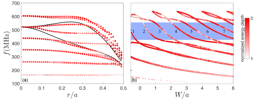
Fig 8(a) shows the eigenfrequency-radius relation of a 5 holes removed supercell (=5), with 3 holes on each side of the cavity (=3), calculated at the limit of the BZ (point X). Between the two black curves is the band-gap region of the perfect PnC. Two cavity modes are already in the band-gap region when r/a is near 0. They are separated with a certain distance as the radius increases. The two modes below penetrate into the band gap and become the cavity modes. It seems that the four cavity modes have a tendency to reach a similar distance from each other, referred to as mode spacing, the same way as the Love modes with r/a close to 0. Once this distance is reached, the lower external modes will cut in and their frequencies will be little affected by the normalized radius of the PnC. The modes outside are disturbed when approaching the band gap, and begin to surround this region. However, a larger radius of the holes and a lower order of the cavity modes result in a deeper mode energy (less confined to the surface), leading to a drop of energy transmission. The lowest cavity mode that appears around =0.45 becomes even difficult to recognize. This explained the different transmission peaks for the and defect-containing PnCs. For this reason, we change the radius of the holes for our PnC to in the rest of this paper, corresponding to a band gap extending from 426.8 to 555.5 MHz.
Fig 8(b) is the eigenfrequency-cavity width relation of a supercell with , calculated at point X. Inside the band gap denoted in blue are the cavity modes. As the cavity width increases, the frequencies of cavity modes decrease and modes with higher order appear (denoted by numbers). Apart the cavity mode, other modes are in pairs, and each pair is twisted outside the band-gap region and mutually merged. In our range of measurement (for from to ), the confinement of Love modes in the band-gap region is better for a larger cavity width () or a squeezed cavity width () . As the order of the cavity modes increases, the modes become less inclined, providing a larger cavity width range for each mode inside the band-gap region. For example, from 1 to 2.3 for the cavity mode, and from 3 to 4.7 for the cavity mode. The wave period in the cavity increases by one-half for every higher mode order.
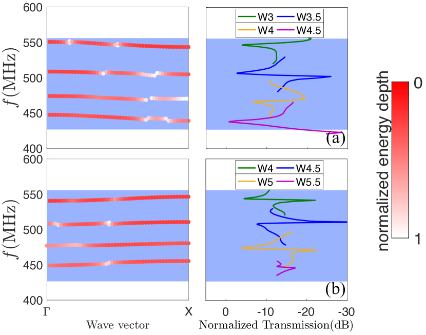
According to the cavity modes predictions in Fig 8(b), the transmission peaks of cavity modes can be displaced inside the band-gap region by changing the width of the cavity. The fifth and sixth cavity modes are shown as examples in Fig 9. As the cavity width increases, the resonant frequency of each cavity mode decreases, with different occurring order of resonance and anti-resonance on the transmission peaks. This proved the possibility of manipulation on the position of transmission peaks. However, significant changes in shape are observed. This can be explained after carefully observing the dispersion curve of each peak. It is found that the group velocity is negative for the 5th cavity mode and is positive for the 6th cavity mode. This is not influenced by the change in cavity width. However, the continuity and homogeneity of the dispersion curves are altered. A well confined (denoted in red) and smooth dispersion curve gives rise to a high and sharp transmission peak, see the cases of and for the 6th mode in Fig 9(b). If the mode is leaky (denoted in white) somewhere in the dispersion curve and causes the curve to break (discontinuity or non-smoothness), the corresponding transmission peak might be affected, in terms of height and/or sharpness. The transmission peak of the 6th mode is perturbed on a cavity, exhibiting a shift at the resonant frequency compared to the dispersion curve, which might be another explication of its shortened peak. A confined mode at point X is hence only a prerequisite for a high and sharp peak. The dispersion curves for the 6th cavity mode are more compact than the curves for the 5th mode, as it possesses a larger range of cavity width within the band gap.
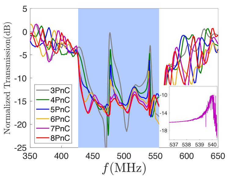
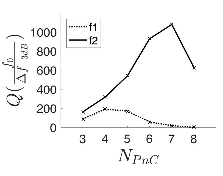
Fig 10 shows the influences of the number of PnC holes (the crystal size) on the formation of peaks. As augments, the band-gap effect increases and it becomes harder for the waves to penetrate through the crystal, so the cavity peaks become shorter and sharper. The 1st transmission peak (at 478 MHz) drops more quickly than the 2nd peak, due to the enhanced band-gap effect in the center of the band-gap region, and eventually disappears after exceeds 7. On the other hand, insufficient crystal size ( below 4) results in the blunt peaks, i.e., insufficient to filter out waves in the band-gap range other than the cavity frequencies. The changes in quality factors (Qs) of the two peaks are shown in Fig 11. As augments, the Qs have a tendency to increase and then decrease. The Q of the 1st resonant mode decreases earlier due to its rapidly shortened peak. The Q of the 2nd peak reaches a maximum (1100) at , where a highly confined cavity mode appears at 540 MHz, shown in the inset of Fig 10. It begins to decrease at , owing to the shortened peak. For this reason, the crystal size should be properly chosen to keep a good quality factor as well as an isolation of the cavity modes. It is further confirmed that in our range of measurement (), the eigenfrequencies of cavity modes are independent of the crystal size, with only slight frequency shifts on the transmission peaks, which is mainly due to the mesh construction of the FEM.
III CONCLUTION
In summary, we have presented the evidence of a partial band gap for Love waves propagating in a PnC consisting of holey square arrayed silica film on a 90ST-cut quartz. Cavity modes in the phononic band gap for Love waves are first demonstrated by removing lines of holes from the guiding film. The transmission peaks of cavity modes in the band gap of the perfect PnC is attributed to the appearance of new flat modes in the band structure. The transmission spectra are proved to be consistent with the band structure predictions. The resonant frequencies of cavity modes are related to the cavity width. A well confined and flat cavity mode, as well as a properly chosen PnC size, is essential for obtaining sharp transmission peaks. This study could be used for potential applications of Love wave-based PnC devices.
REFERENCES
References
- [1] A. Khelif, A. Choujaa, B. Djafari-Rouhani, M. Wilm, S. Ballandras, and V. Laude, Physical Review B 68 (2003).
- [2] A. Khelif, A. Choujaa, S. Benchabane, B. Djafari-Rouhani, and V. Laude, Zeitschrift für Kristallographie - Crystalline Materials, 220 836–840 (2005).
- [3] T.-C. Wu, T.-T. Wu, and J.-C. Hsu, Physical Review B 79, 836–840 (2009).
- [4] R. H. Olsson, S. X. Griego, I. El-Kady, M. Su, Y. Soliman, D. Goettler, and Z. Leseman, in IEEE International Ultrasonics Symposium (2009), pp. 1150-1153.
- [5] Y. Pennec, J. O. Vasseur, B. Djafari-Rouhani, L. Dobrzyński, and P. A. Deymier, Surface Science Reports 65, 229-291 (2010).
- [6] B. Liang, X. S. Guo, J. Tu, D. Zhang, and J. C. Cheng, Nature Materials 9, 989-992 (2010).
- [7] D. Feng, W. Jiang, D. Xu, B. Xiong, and Y. Wang, Applied Physics Letters 110, 171902 (2017).
- [8] F. Meseguer, M. Holgado, D. Caballero, N. Benaches, J. Sánchez-Dehesa, C. López, and J. Llinares, Physical Review B 59, 12169-12172 (1999).
- [9] T. T. Wu, W. S. Wang, and J. H. Sun, in IEEE International Ultrasonics Symposium (Nov. 2008), pp. 709-712.
- [10] R. H. Olsson III and I. El-Kady, Measurement Science and Technology 20, 012002 (2009).
- [11] M. Ziaei-Moayyed, M. F. Su, C. Reinke, I. F. El-Kady, and R. H. Olsson, in IEEE 24th International Conference (2011), pp. 1377- 1381.
- [12] T.-W. Liu, Y.-C. Tsai, Y.-C. Lin, T. Ono, S. Tanaka, and T.-T. Wu, AIP Advances 4, 124201 (2014).
- [13] L. Binci, C. Tu, H. Zhu, and J. E.-Y. Lee, Applied Physics Letters 109, 203501 (2016).
- [14] A. Talbi, F. Sarry, M. Elhakiki, L. L. Brizoual, O. Elmazria, P. Nicolay, and P. Alnot, Sensors and Actuators A: Physical 128, 78-83 (2006).
- [15] R. Lucklum and J. Li, Measurement Science and Technology 20, 124014 (2009).
- [16] M. Ke, M. Zubtsov, and R. Lucklum, Journal of Applied Physics 110, 026101 (2011).
- [17] M. Zubtsov, R. Lucklum, M. Ke, A. Oseev, R. Grundmann, B. Henning, and U. Hempel, Sensors and Actuators A: Physical 186, 118-124 (2012).
- [18] A. Salman, O. A. Kaya, A. Cicek, and B. Ulug, Journal of Physics D: Applied Physics 48, 255301 (2015).
- [19] Z. Xu and Y. J. Yuan, Biosensors and Bioelectronics 99, 500–512 (2018).
- [20] B. Kim, J. Nguyen, C. Reinke, E. Shaner, C. T. Harris, I. El-Kady, and R. H. Olsson III, in IEEE International Ultrasonics Symposium (Oct. 2011), pp. 1308-1311.
- [21] J.-K. Yu, S. Mitrovic, D. Tham, J. Varghese, and J. R. Heath, Nature Nanotechnology 5, 718–721 (2010).
- [22] L. Yang, N. Yang, and B. Li, Nano Letters 14, 1734-1738 (2014).
- [23] N. Zen, T. A. Puurtinen, T. J. Isotalo, S. Chaudhuri, and I. J. Maasilta, Nature Communications 5 (2014).
- [24] X. Zhang and Z. Liu, Applied Physics Letters 85, 341-343 (2004).
- [25] D. M. Profunser, E. Muramoto, O. Matsuda, O. B. Wright, and U. Lang, Physical Review B 80 (2009).
- [26] J. Zhu, J. Christensen, J. Jung, L. Martin-Moreno, X. Yin, L. Fok, X. Zhang, and F. J. Garcia-Vidal, Nature Physics 7, 52-55 (2011).
- [27] S. Narayana and Y. Sato, Physical Review Letters 108 (2012).
- [28] J. Zhao, B. Bonello, R. Marchal, and O. Boyko, New Journal of Physics 16, 063031 (2014).
- [29] J. Li, F. Wu, H. Zhong, Y. Yao, and X. Zhang, Journal of Applied Physics 118, 144903 (2015).
- [30] C.-N. Tsai and L.-W. Chen, Applied Physics A 122 (2016).
- [31] J. H. Page, AIP Advances 6, 121606 (2016).
- [32] Y. Guo, D. Brick, M. Gromann, M. Hettich, and T. Dekorsy, Applied Physics Letters 110, 031904 (2017).
- [33] R. Martínez-Sala, J. Sancho, J. V. Sánchez, V. Gómez, J. Llinares, and F. Meseguer, Nature 378, 241–241 (1995).
- [34] Z. Liu, X. Zhang, Y. Mao, Y. Y. Zhu, Z. Yang, C. T. Chan, and P. Sheng, Science 289, 1734–1736 (2000).
- [35] J. O. Vasseur, P. A. Deymier, B. Chenni, B. Djafari-Rouhani, L. Dobrzynski, and D. Prevost, Physical Review Letters 86, 3012– 3015 (2001).
- [36] S. Yang, J. H. Page, Z. Liu, M. L. Cowan, C. T. Chan, and P. Sheng, Physical Review Letters 88 (2002).
- [37] L. Dhar and J. A. Rogers, Applied Physics Letters 77, 1402 (2000).
- [38] T.-T. Wu, L.-C. Wu, and Z.-G. Huang, Journal of Applied Physics 97, 094916 (2005).
- [39] A. Khelif, B. Aoubiza, S. Mohammadi, A. Adibi, and V. Laude, Physical Review E 74 (2006).
- [40] S. Mohammadi, A. A. Eftekhar, A. Khelif, W. D. Hunt, and A. Adibi, Applied Physics Letters 92, 221905 (2008).
- [41] S. Benchabane, O. Gaiffe, G. Ulliac, R. Salut, Y. Achaoui, and V. Laude, Applied Physics Letters 98, 171908 (2011).
- [42] Y. Achaoui, V. Laude, S. Benchabane, and A. Khelif, Journal of Applied Physics 114, 104503 (2013).
- [43] T.-W. Liu, Y.-C. Lin, Y.-C. Tsai, T. Ono, S. Tanaka, and T.-T. Wu, Applied Physics Letters 104, 181905 (2014).
- [44] S. Hemon, A. Akjouj, A. Soltani, Y. Pennec, Y. El Hassouani, A. Talbi, V. Mortet, and B. Djafari-Rouhani, Applied Physics Letters 104, 063101 (2014).
- [45] M. Torres, F. R. Montero de Espinosa, and J. L. Aragfffdfffdn, Physical Review Letters 86, 4282–4285 (2001).
- [46] R. H. Olsson, I. F. El-Kady, M. F. Su, M. R. Tuck, and J. G. Fleming, Sensors and Actuators A: Physical 145-146, 87–93 (2008).
- [47] S. Mohammadi, A. A. Eftekhar, W. D. Hunt, and A. Adibi, Ap- plied Physics Letters 94, 051906 (2009).
- [48] Y. Jin, N. Fernez, Y. Pennec, B. Bonello, R. P. Moiseyenko, S. H ̵́emon, Y. Pan, and B. Djafari-Rouhani, Physical Review B 93 (2016).
- [49] A. Khelif, P. A. Deymier, B. Djafari-Rouhani, J. O. Vasseur, and L. Dobrzynski, Journal of Applied Physics 94, 1308–1311 (2003).
- [50] Y. Pennec, B. Djafari-Rouhani, J. O. Vasseur, H. Larabi, A. Khe- lif, A. Choujaa, S. Benchabane, and V. Laude, Applied Physics Letters 87, 261912 (2005).
- [51] S. Benchabane, O. Gaiffe, R. Salut, G. Ulliac, V. Laude, and K. Kokkonen, Applied Physics Letters 106, 081903 (2015).
- [52] T. Miyashita, Measurement Science and Technology 16, R47– R63 (2005).
- [53] S. Yankin, A. Talbi, Y. Du, J.-C. Gerbedoen, V. Preobrazhensky, P. Pernod, and O. Bou Matar, Journal of Applied Physics 115, 244508 (2014).