Characterisation of a large area silicon photomultiplier
Abstract
This work illustrates and compares some methods to measure the most relevant parameters of silicon photo-multipliers (SiPMs), such as photon detection efficiency as a function of over-voltage and wavelength, dark count rate, optical cross-talk, afterpulse probability. For the measurement of the breakdown voltage, , several methods using the current-voltage curve are compared, such as the “IV Model”, the “relative logarithmic derivative”, the “inverse logarithmic derivative”, the “second logarithmic derivative”, and the “third derivative” models. We also show how some of these characteristics can be quite well described by few parameters and allow, for example, to build a function of the wavelength and over-voltage describing the photodetection efficiency. This is fundamental to determine the working point of SiPMs in applications where external factors can affect it.
These methods are applied to the large area monolithic hexagonal SiPM S10943-2832(X), developed in collaboration with Hamamatsu and adopted for a camera for a gamma-ray telescope, called the SST-1M. We describe the measurements of the performance at room temperature of this device. The methods used here can be applied to any other device and the physics background discussed here are quite general and valid for a large phase-space of the parameters.
keywords:
SiPM, MPPC, , , cross-talk, dark count rate, afterpulses, triggering probabilityMSC:
[2010] 00-01, 99-001 Introduction
In the last few years the interest in solid state photodetectors has grown significantly. In particular, SiPMs 111Hamamatsu adopted the name Multi-Pixel Photon Counters or MPPCs have replaced traditional photo-multiplier tubes (PMTs) in many applications. As a matter of fact, they are very compact, robust, lightweight, insensitive to magnetic fields and work at temperatures that span a wide range from cryogenics to beyond room temperature. Their operating parameters are stable across devices of the same type thanks to the high level of uniformity achieved by the solid state technology production technique. Also the absence of aging caused by the integrated light over time, makes them particularly tailored for ground-based astrophysics [1], where they can be operated even in the presence of high background light level, thus increasing the duty cycle and then the physics reach of experiments [2].
The University of Geneva and a Consortium of Polish and Czech Institutions have proposed and built a single mirror small size telescope (SST-1M) for the Cherenkov Telescope Array (CTA), equipped with a SiPM-based camera. To achieve the desired performance with the chosen optics, a mirror of 4 m diameter, the camera of the SST-1M is composed by 1296 pixels, each of an angular opening of about . This translates into a pixel linear size of about 2.32 cm (more details on camera and its design and performances can be found in ref. [3]).
In order to have a spatial uniform response of the camera, the pixels should have a circular shape to ensure equal distance between pixel centres in every direction. The hexagon is the best possible shape to achieve this uniformity with minimum dead space. The pixel size to achieve the required angular resolution is achieved through a large SiPM coupled with light funnel. A light funnel, approaching the ideal Winston cone geometry, was designed by the University of Geneva group to be coupled to SiPMs and achieve the desired pixel size. The light funnel has hexagonal shape and has a compression factor of about six [4]. Its internal surface is coated in order to maximise reflection of UV Cherenkov light produced by the cosmic rays when traversing the atmosphere, and also to have a good reflectivity for light with a direction almost parallel to cone surface.
The Winston cone geometry, on the other side, imposes to have the same shape at entrance and exit side and then an hexagonal sensor was needed. This was developed by the University of Geneva group in cooperation with the Hamamatsu company (Hamamatsu S10943-2832(X)). The main characteristics of the sensor are detailed in Tab. 1. The sensor area is around 93.6 mm2 with a linear dimension of 10.4 mm flat-to-flat. It ranks among the world’s largest monolithic sensor. The large area can be a limiting factor in many application. As matter of fact, the capacitance and the dark-count rate () are proportional to SiPM area. Hence, larger devices tend to have longer output signals and be more noisy. However, as shown by the SST-1M camera [3], with the proper electronics, such a large device can achieve the desired performances in specific applications.
This work reports on the characterization studies done to validate the design and verify the performances of the SST-1M new sensor type.
| Nr. of channels | 4 |
|---|---|
| Cell size | 50 50 m 2 |
| Nr of cells (per channel) | 9210 |
| Fill Factor | 61.5% |
| (@ per channel) | 2.8-5.6 MHz |
| (@ per channel) | 85 fF |
| Cross-talk (@ per channel) | 10% |
| Temp. Coeff. | 54 mV/C∘ |
| Gain (@ per channel) |
2 The Hamamatsu S10943-2832(X) SiPM
The SiPM S10943-2832(X), shown in Fig. 1, has been designed in collaboration with Hamamatsu and is based on the so called LCT2 (Low cross-talk) technology available when the camera design was done. Hamamatsu has further improved this technology (LCT5 or LVR) and offers now better performance. It is worth to mention that the hexagonal shape can be obtained using any Hamamatsu cell standard technology and size, through a dedicated photo-mask. Currently, we evaluate that the slightly higher DCR of LCT2 does not impact significantly performances of camera if appropriately calibrated. Actually, dark counts are useful for in-situ calibrations and then a further reduction of this rate increases the time needed to accumulate the statistics needed for precise calibrations.
The sensor capacitance is directly related to its active area and this has an impact on the signal recharge time. In this case, signals would have typical duration of about hundred ns, a too long time for the desired bandwidth of 250 MHz. This frequency has been chosen taking into account the typical time duration of atmospheric showers induced by gamma-rays and cosmic rays. To reduce the effect of the capacitance, the sensor has four independent anodes and a common cathode as shown in Fig. 1. This configuration allows to readout the 4 channels independently but there is a single bias for the whole sensor. Nonetheless, in order to achieve the desired bandwidth, a shaping of the signal is needed.
To address this features, we developed in house the pre-amplification chain based on off-the-shelf components. The solution adopted [5] is a trans-impedance amplifier topology with low noise amplifiers (OPA846) as it can achieve the required events rate with the best signal-to-noise ratio and gain/bandwidth ratio. As shown in Fig. 2, the four channels are summed by two in order to reduce the equivalent capacitance and pulse length. The summed signals are further summed up in a differential amplifier, which feeds the output signal into the digital readout system.
Another important characteristic of the camera architecture is the fact that the front-end and the digital readout are DC coupled. This is important for gamma-ray astronomy, where Moon light and human-induced light and their reflections are a relevant background. As a matter of fact, the Night Sky Background (NSB) contributes to the determination of the real working point of the device, relevant to correctly extract the number of photons from the signal.
3 Static characterisation
All the laboratory measurements (i.e. static, dynamic and optical) are performed at room temperature T = 25 ∘C at the premises of IdeaSquare222http://ideasquare.web.cern.ch at CERN, where an experimental setup has been developed. The static characterization (i.e. reverse and forward current-voltage (IV) curves), is performed using a Keithley 2400 [6] pico-ammeter for bias supply and current measurements.
3.1 Forward IV characterization
The forward IV characteristic curve of the SiPM, shown in Fig. 3, exhibits a very small increase of the current when the polarization voltage, , is below the threshold value and a linear rapid current increase with above this threshold. A physical interpretation of this behaviour can be attempted starting from the ideal Shockley law [7], which expresses the forward current flowing through a p-n diode as:
| (1) |
where is the diode reverse bias saturation current, is the voltage across the junction, is the thermal voltage and is the ideality factor. The voltage is the difference between the applied voltage and the voltage drop across the neutral region and the ohmic contacts on the two sides of the junction:
| (2) |
where usually 100 .
Replacing by in Eq. 1, we obtain:
| (3) |
The SiPM is an array of micro-cells (cells), which are SPADs (single photon avalanche diode). Each cell can be represented by a diode connected in series with a quenching resistor 333The cell works in Geiger-Avalanche mode meaning that when a photon is absorbed, an electron-hole pair is created and the high electric field in the junction starts charge multiplication, which produces an avalanche. If the field is not reduced, the charge avalanche is stationary and leads to thermal destruction of the device. By adding a resistor in series to the cell, a voltage drop is produced by the current induced by the charge avalanche when flowing into the resistor. This drop reduces the field across the device thus quenching the avalanche. For this reason the SiPM are also referred to as an array of G-APDs - Geiger-Avalanche Photo-Diodes.. Eq. 3 applies to each single cell but requires the addition of the voltage drop caused by the presence of a quenching resistance . Then for a full SiPM device with connected in parallel, Eq. 3 becomes:
| (4) |
where is the SiPM reverse bias saturation total current and is the forward total current flowing through it.
The last term of Eq. 4 becomes dominant when the current is high ( 5 A). In this regime, + can be extracted from a linear fit of the forward IV characteristic curve in Fig. 3:
| (5) |
where is the slope parameter extracted by the linear fit (red line in Fig. 3). Also, can be calculated as . For this SiPM, the fit gives (stat.) (sys.) k. The systematic uncertainty comes from the fact that does not increase linearly with . This can be seen from the bottom part of Fig. 3, showing and . It is calculated as:
| (6) |
where and are two slopes calculated at of 1.6 V and 2.5 V respectively.
3.2 Reverse IV characterisation
The current flowing in the SiPM, when not illuminated, depends on the available free carriers. The Shockley-Read-Hall (SRH) [8, 9] effect is the dominant one in semiconductors and it is also the main contribution to the bulk dark current. It describes the generation and recombination of electron-hole pairs due to the trapping effect of impurities in the lattice (for this also called trap-assisted recombination), as well as band-to-band tunneling effects. In addition the carriers generation rate can be enhanced by reduction of activation energy due to the Poole-Frenkel effect [10].
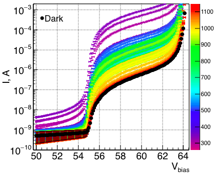
In the reverse IV characteristic curve of the SiPM, shown in Fig. 4, two zones are identified, corresponding to different regimes:
-
(1)
the “Linear” regime (pre-breakdown), corresponding to below the breakdown voltage (), where the current increases slowly with . This dark current is due to the surface current and the bulk dark current due to the free carriers.
-
(2)
the “Geiger” regime (post-breakdown), corresponding to above where the current increases much faster with . This trend is due to the Geiger avalanche created by the free carriers generated by ionization. Primary free carriers, which trigger an avalanche, are usually created, due to the SRH thermal generation enhanced by Poole-Frenkel effect and tunnelling, but also to other associated effects as afterpulsing, prompt cross-talk and delayed cross-talk.
The breakdown voltage of a SiPM device represents the voltage above which the electrical field inside the depleted region of a cell is high enough that any free carrier (created by an absorbed photon or by a thermally generated carrier) can trigger an avalanche. It marks, then, the transition between the two regimes and that is why it represent one of the most important parameter to determine.
The reverse IV measurements is commonly used for fast calculation of using different methods such as the “relative logarithmic derivative” [11], the “inverse logarithmic derivative” [12], the “second logarithmic derivative” [13], the “third derivative” [14] and “IV Model” methods [15, 16].
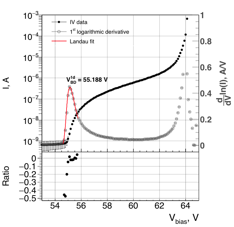
In the “relative logarithmic derivative” the breakdown voltage can be calculated [17] as the voltage where diverges, where is the model constant which determine the shape of the reverse . Clearly, this divergence is not observed in the experimental data, being a non-physical state. Therefore, from this method one can extract , a quantity proportional to , as the voltage at which the “relative logarithmic derivative” has a local maximum, for example by fitting the region around with a peaked and skewed function. In our case, we chose a Landau function (see Fig. 5).
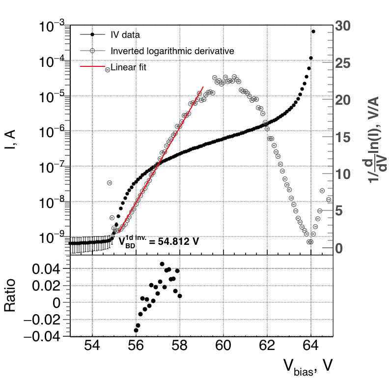
The “inverse logarithmic derivative” increases linearly with above the (See Fig. 6). Assuming that this behaviour does not change near the breakdown region, the breakdown voltage can be extracted as the voltage at which the “inverse logarithmic derivative” is equal to zero, i.e. the intersection with the x-axis of the fitted line above .
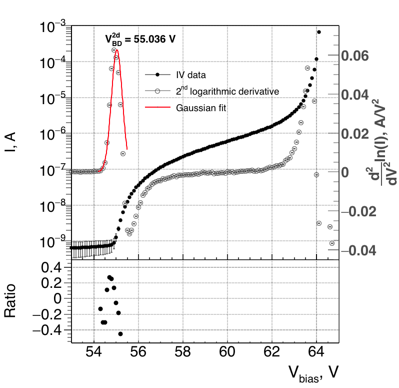
The “second logarithmic derivative” method [13, 18] is commonly used for the determination. Here, is calculated as the voltage corresponding to the maximum of the second derivative, as shown in Fig. 7. However, we observe that the Gaussian fit does not describe the data well. Therefore, this method determines a systematic error in the absolute value of .
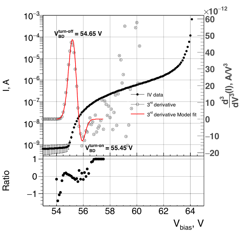
The “third derivative” method [19, 14] assumes two separate breakdown voltages: the “turn-on” and “turn-off” voltages. defines the regime in which a cell initiates an avalanche and the current is related to the avalanche triggering probability . is the voltage at which the quenching of the avalanche starts and the current is related to charge production. Following the prescription in Ref. [14], we find 54.65 V and 55.45 V for and , respectively (see Fig. 8).
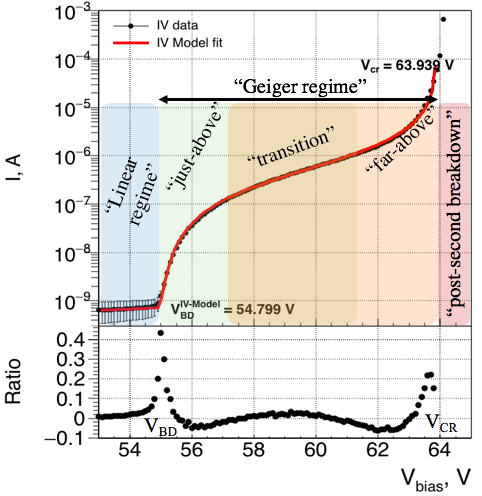
To overcome the limitation of all the methods shown so far, a model of the reverse IV curve has been proposed [15, 16]. According to this “IV Model”, different SiPM working regimes can be identified in the IV curve, as shown in Fig. 9. As in Fig. 4 the “Linear” region (1) is below , while here the “Geiger” region above , is split in four different regions: the “just-above” (breakdown), “transition”, “far-above” and “post-second breakdown” zones.
This model can describe the IV over the full working range of SiPM and therefore it can be used not only to determine breakdown voltage , but also to determine other SiPM parameters such as working range or Geiger probability when the IV is measured under light illumination. Here we use the procedure described in Ref. [15], and we obtain a V.
The systematic uncertainty on all these measurements is given by the:
- 1.
-
2.
the model assumptions made to approximate the IV curve with a simple equation:
-
(a)
as already noted, divergence to infinity of the reverse IV for the “relative logarithmic derivative” and for the “inverse logarithmic derivative” cannot physically observed;
-
(b)
“second logarithmic derivative” and “third derivative” methods do not fit perfectly experimental data;
-
(c)
the ”IV Model” does not describe the experimental data near and . As a matter of fact, a SiPM biased below works like an avalanche photodiode and this regime is not included in the IV Model (for more details see Ref. [16]). Additionally, following Ref. [20], the value is subject to statistical fluctuations due to Geiger avalanche statistical fluctuations. On the other hand, the difference near is related to the voltage drop on .
-
(a)
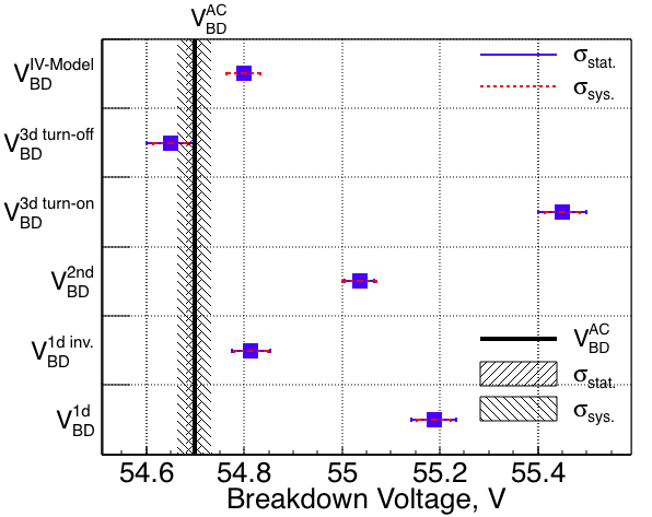
In Fig. 10, the values of obtained using the described methods are compared. They are spread over a range of less than 1 V. In general, the “inverse logarithmic derivative” or “second logarithmic derivative” methods provide the most stable and straightforward results, and provide a reasonable estimate of . Therefore, those methods are used when many SiPM devices should be characterized or compared, as for example in quality assurance procedures. However, for the full characterization of a device, the ”IV model” should be used, as it can provide the most complete description of the reverse IV. This is the optimal method when design and tuning of front-end electronics is needed or to compare performance of different devices. Moreover, as will be shown in Sec. 5.2, the “IV Model” method can also provide the relative photodetection efficiency () of a device.
4 Dynamic characterisation
For the dynamic measurements presented here (also refereed further as AC measurements), instead of the standard pre-amplification topology used in the real camera [5](see Fig. 2), each SiPM channel is connected to an operational amplifier OPA846 and readout independently. The SiPM device is illuminated with low intensity light of different wavelengths (e.g. 405 nm, 420 nm, 470 nm, 505 nm, 530 nm and 572 nm) produced by pulsed LEDs. For each operating voltage of the LED providing a certain light level, 10’000 waveforms are acquired on an oscilloscope and sampled at 500 MHz. Each one is 10 s long. The signal used to pulse LEDs is produced by a pulse generator and it is also used to trigger waveform acquisition.
The readout window is adjusted in such a way to have the trigger signal in the middle of the waveform. i.e. at 5 s from the window start, in order to have
-
1.
a “Dark” interval from 0 to 5 s, when the device is operated in dark conditions. Only uncorrelated enhanced by correlated noise, i.e. cross-talk (prompt and delayed) and afterpulses, are present (see Sec. 4.5 for more details);
-
2.
“LED” interval, from 5 to 10 s, when the device is illuminated by LED light pulses. In this case, both signals pulses due to the light and uncorrelated SiPM noise pulses are present. Both types of pulses are further affected by SiPM correlated noise (i.e. prompt and delayed cross-talk and afterpulses).
Dark intervals are used to calculate the SiPM , the breakdown voltage , the dark count rate () and the optical cross-talk probability , while LED intervals are used to calculate the SiPM photon detection efficiency . To measure the afterpulses probability , an additional data run was performed (See sec. 4.5.2).
The data acquisition system used for these measurements, consists of a transimpedance amplifier based on OPA846, an oscilloscope Lecroy 620Zi for the waveform acquisition (a bandwidth of 20MHz is used to reduce the influence of the electronic noise) and a Keithley 6487 to provide bias voltage to the SiPM. For each LEDs of different wavelengths, the over-voltage = is varied in the range 1 V V, to cover the full working range of the device (see Sec. 3.2).
4.1 Automatic data analysis procedure
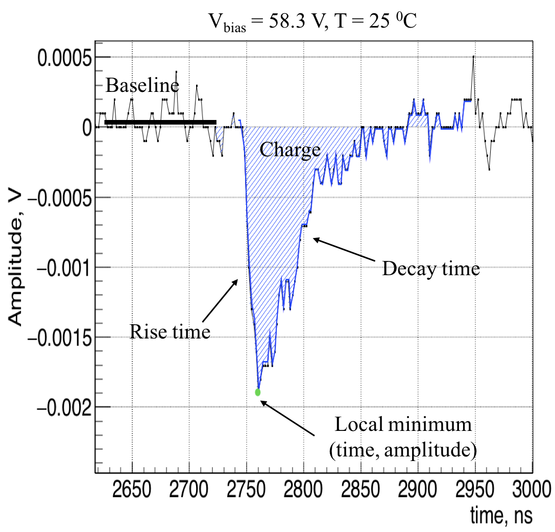
The acquired experimental data are analyzed with an automatic procedure developed in the ROOT Data Analysis Framework 444https://root.cern.ch. The waveforms acquired with the oscilloscope are used to create ntuples storing SiPM pulse templates. The steps of the analysis to determine the main features of pulses are the following:
-
1.
the construction of a template of a typical SiPM pulse shape (see Fig. 11) in a given working condition;
-
2.
a pulse finding procedure to identify SiPM pulses (i.e. a single pulse or a train of pulses 555By single pulses here it is intended a SiPM signal separated by neighbouring pulses by a time interval longer than its recovery time, while train of pulses is a sequence of two or more signals within a time interval shorter than the SiPM recovery time.) and their relative time spacing;
-
3.
a template subtraction to reconstruct only the SiPM pulses in a train of pulses.
The SiPM pulse characteristics, such as the baseline, time position and amplitude, rise time and decay time, charge , 666Time difference between the analyzed pulse and the previous one. and 777Time difference between the analyzed pulse and the following one., are determined for different values of . More details on the developed analysis procedure can be found in the Ref.[21].
4.2 SiPM Gain
The SiPM gain is defined as the number of charges created by one avalanche in one and it can be expressed as:
| (8) |
where is the avalanche charge, and are the and parasitic capacitance, respectively, and is the breakdown voltage (more details are given in Sec. 4.3). The SiPM gain can be calculated from the time integration of the signals of a device:
| (9) |
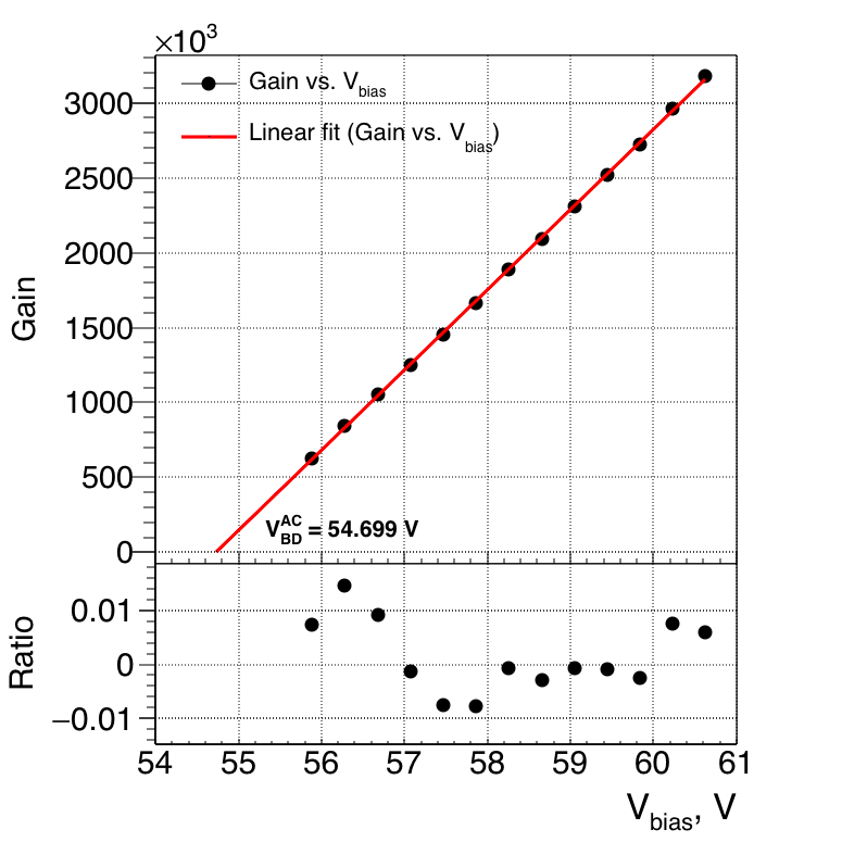
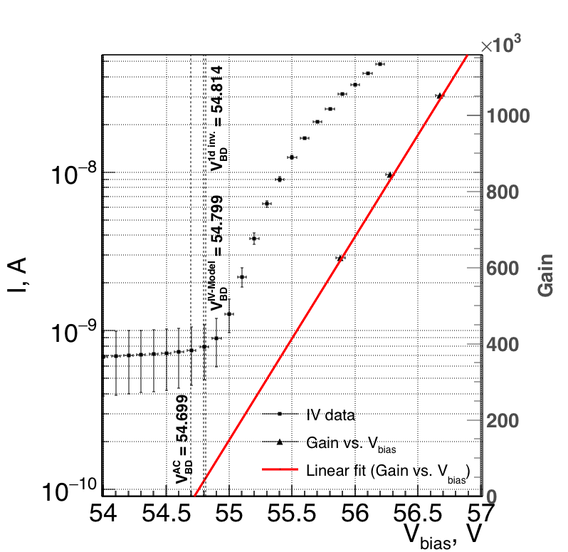
where is the amplifier gain, is the amplifier input impedance (), is the pulse evolution over time and is the baseline. The gain of the OPA846 amplifier has strong frequency dependence. Therefore, it will be different for different SiPMs. However, in particularly for our SiPM device the of 5.86 0.04 was found. At a given and temperature the SiPM gain has Gaussian shape as shown in [22]. Therefore, gain errors were calculated as the errors of the mean. As can be seen in Fig. 12, the gain increases linearly with as expected from Eq. 8.
4.3 Breakdown Voltage
From the curve of the gain as a function of (Fig. 12), the breakdown voltage can be determined as the value where (see Eq. 8), i.e. extrapolating the linear fit to zero. The obtained value is = 54.699 0.017 (stat.) 0.035 (sys.) V. The comparison between this value and those obtained from reverse IV curve static methods (see Sec. 3.2) is shown in Fig. 10. We can observe significant differences between the dynamic measurement and the static ones, except for the obtained with the derivative method. The and are equal within the uncertainties. However, for all other breakdown voltages, the value is a few hundreds of smaller than from the IV methods. This discrepancy reflects the described limitation of some of the static methods. As it can be seen in Fig. 13, the static measurement is sensitive to the onset of the avalanche phenomenon and it determines the breakdown voltage, as defined by the fundamental papers of McIntyre (named as “turn-on” voltage) [23]. The linearity dynamic method determines the voltage across the diode when the avalanche is quenched (named as “turn-off” voltage). The “turn-off” (i.e. and ) is naturally lower than the “turn-on” (i.e. , , , and ), as shown in the Fig. 10).
4.4 SiPM micro-cell capacitance and depletion depth
Combining Eq. 8 and Eq. 9, one can extract the device capacitance, which is the sum of the cell capacitance and the parasitic one. is related to cell geometry, through the parallel plane capacitance equation:
| (10) |
where = F/cm is the vacuum permittivity, = 11.9 is the silicon dielectric constant, m2 is the active area reduced by the geometrical fill factor of 0.615 and is the depletion thickness of the cell. From this formula, the resulting depletion thickness is m. This relationship between and the depletion thickness was studied with Silvaco TCAD888https://www.silvaco.com/products/tcad.html simulation of the capacitance-voltage characteristic of a diode structure similar to the SiPM micro-cell (i.e. p+/n/n-epi/n-substrate). We found agreement between simulated and calculated depletion thicknesses within 0.1 m, corresponding to 5.2 relative error.
4.5 SiPM noise and
SiPM noise is a limiting factor for low-light level applications (from one to few photons) and various mechanisms contribute to it. Two main categories of noise can be identified: the or primary uncorrelated noise, which is independent from light conditions, and the secondary or correlated noise.
At room temperatures, the is dominated by thermal generation of carriers. When a SiPM is operated at high overvoltage and the electric field across the junction increases, the carriers can tunnel from the valence band to the conduction band through trap or defect states. In this case, the rate of thermally generated carriers is amplified by the trap-assisted tunnelling mechanism. In addition, the generation rate can be enhanced by the reduction of activation energy due to the Poole-Frenkel effect [10]. As the electric field increases, the tunnelling of electrons directly from the valence band into the conduction band increases. Therefore, at a given temperature, the is determined by the rate of thermally generated carriers and the probability that carriers trigger an avalanche (i.e. Geiger probability ). Consequently, a simple empirical formula for the can be approximated as:
| (11) |
where is a free parameter describing the increase of with due to electrical field effects, is the average Geiger probability for dark pulses. Following the Refs. [15] [24] the Geiger probability can be well expressed as:
| (12) |
where is the SiPM structural parameter, which determines the rate of increase of with . depends on whether an electron or a hole initiates an avalanche (i.e. it detected light of some wavelength) and to some extent on the temperature [25] (See Sec. 5.3). Therefore, can be approximated as:
| (13) |
where is the average of pulses.
Secondary, or correlated, noise is due to the optical cross-talk and the afterpulsing induced by a primary avalanche previously generated by a noise source or by detected light photons. During the primary avalanche multiplication process, photons can be emitted due to hot carrier luminescence phenomena [26]. These photons may lead to:
-
1.
Prompt optical cross-talk, due to photons starting secondary avalanches in one or more neighbour cells. Therefore, the prompt cross-talk probability can be expressed as:
(14) where is the probability that a photons is emitted, reach the high field region of another cell and create electron-hole pair, is the SiPM gain, i.e. the number of charges created during primary avalanche multiplication (see Eq. 8) and is the average Geiger probability for cross-talk pulses. can be approximated as:
(15) where is the average of cross-talk pulses.
- 2.
Afterpulsing occurs when, during the primary avalanche multiplication process, carriers are captured by trap levels in the cell junction depletion layer and are released after some time, triggering a secondary avalanche discharge correlated to the primary one. Therefore, the afterpulse probability can be approximated as:
| (16) |
where is the probability that a carrier will be trapped and released after and is the average Geiger probability for afterpulses.
Since, the afterpulsing occurs in the same cell as primary avalanche, its amplitude strongly depends on the recovery state of the cell, and can be expressed as:
| (17) |
where is the single photoelectron (p.e.) amplitude and is the recovery time constant.
As mentioned before, the device is considered as operated in dark conditions, in the time window of about 5 s preceding the LED trigger. This time interval is used to calculate the dark count rate .
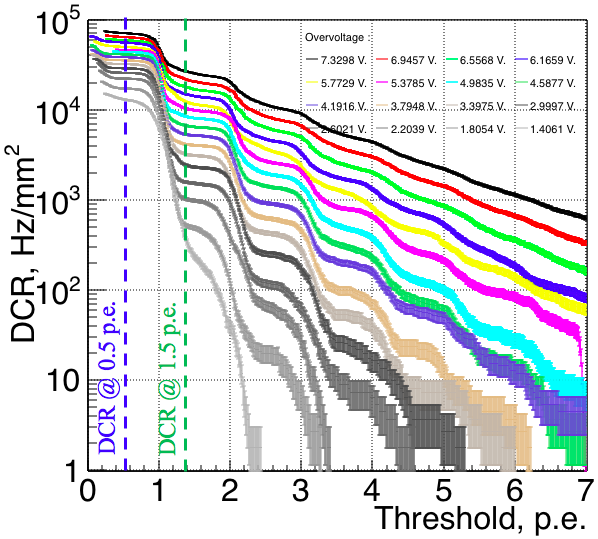
The as a function of a discriminating threshold expressed in photoelectrons at a given is calculated by counting the number of SiPM pulses with amplitude above the threshold (see Fig. 14). This counting method is affected by afterpulses. To overcome this limitation, the Poisson statistic can be used to calculate pure uncorrelated SiPM noise at 0.5 p.e. threshold as:
| (18) |
where is the Poisson probability not to have any SiPM pulse and then is the average number of detected SiPM pulses within the time interval . The can be calculated as:
| (19) |
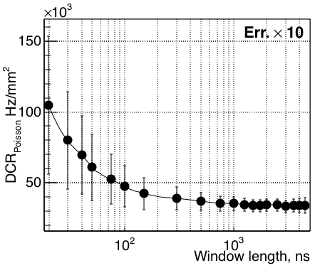
where (total) represents the total number of analyzed waveform and (0) is the number of waveforms without any SiPM pulse within given time interval . As can be seen in Fig. 15, the is overestimated for short window lengths ( 1 s), as it also affected by afterpulses. So to estimate correctly the DCR, we need to use a window greater than 1 s, where the DCR becomes flat within the error bars. This value clearly depends on the afterpulse probability and their distribution in time for the specific device, but the same method can be used to identify the right window size for any type of device.
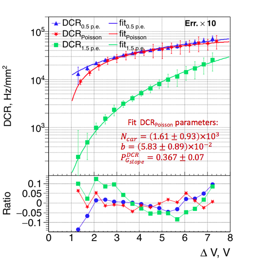
Despite the fact that calculated from pulse counting method is slightly overestimated due to afterpulses (see Fig. 16), it is anyhow interesting to use it to extract other important parameters of the device.
The trend of the measured as function of the overvoltage, at the threshold of 0.5 p.e., can be fitted using Eq. 11. From the fit, we can extract using Eq. 13 (for a physical interpretation of this parameter see Sec. 5.3). The discrepancy between data and fit is larger than the errors. This can be related to the fact that the fit formula does not include afterpulses and delayed optical cross-talk. The inclusion of these two effects would make the fit more complex and unstable. This inclusion is not worth given that the errors are quite small (10 ppm at V) and then the discrepancy has negligible impact.
4.5.1 Prompt cross-talk probability
The measured at thresholds 1.5. p.e. can be regarded as the results of the optical cross-talk effects related to the and then
| (20) |
which can be used to define how to measure :
| (21) |
However also the pile up effect is present. The total rate of pile up pulses within a given time interval can be calculated as the sum of the pile up rate of two, three, four and more pulses (). Using a standard approach [29], the rate for the estimation of accidental pile up of 2 pulses, with a rate of and a coincidence window of , is . Therefore, the total rate, , for any number pile-up event, can be regarded as a geometrical series of :
The can be corrected for the pile up effect as:
| (23) |
In our case, the afterpulses can be neglected as they can appear within , and then their contribution to the amplitude is negligible. As matter of fact, the maximum possible afterpulse amplitude within this time interval was calculated from Eq. 17 and it is only 0.37 p.e. Therefore, the amplitude of the primary pulse, even including afterpulses, is still below 1.5 p.e. threshold.
In Fig. 17 the prompt optical cross-talk probability, , as a function of the over-voltage, , is shown (blue dots) together with the corrected one (green dots). The pile-up correction is below 1% due to the small value of , which is the minimal separation in time between two pulses needed for the automatic data analysis to recognize them as single pulses inside a train. However, the pile-up correction may become important when SiPMs with very low are used or when is much longer, as shown in Ref. [30].
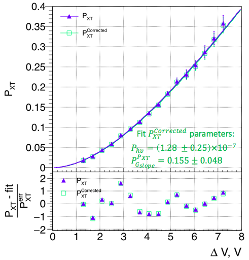
We can see that except for two points, the difference between fit and data is inside the error bars. Given fF (See Tab. 1), two free parameters can be extracted from the fit of : and . We find an average probability that photon with sufficient energy can be emitted by one carrier crossing the junction during avalanche multiplication and reach the high field region of another cell. Taking into account that the average probability of photons with energy higher than 1.14 eV (or ), emitted by carriers crossing the junction, is [31], we can conclude that around 2% of emitted photons reach the high field region of neighbouring cells. The parameter is extracted from the fit. Its physical interpretation will be discussed later in section 5.3.
As a further cross-check, we use the value found here for to fit the data in Fig. 16 using Eq. 20 and Eq. 14. The parameters found from the fit of in Fig. 16 are fixed in the fit for . Also in this case, the data are well reproduced by the fitted model, as for
The , extracted from data shown in Fig. 16, represents the probability that a free carrier initiates an avalanche (see Eq. 11), while represents the probability that a photon (emitted by hot carrier luminescence) is absorbed and initiate an avalanche (See Eq. 14). In general, free carriers and luminescence photons are absorbed at different depths of SiPM active areas. Therefore, , even if they have a similar behaviour as a function of .
4.5.2 Afterpulse and delayed cross-talk probability
The afterpulse probability is measured by acquiring 20 s long waveforms, triggering their acquisition and using a pulse with an amplitude larger than 0.5 p.e.. This pulse, called in the following primary pulse, is adjusted to fall in the center of the waveform (i.e. at 10 s). To ensure that pulses are either afterpulses related to the primary pulse or randomly generated dark pulses, waveforms without any signal within the 5 s preceding the primary pulse are selected and analyzed in the following. For all waveforms triggered by a primary signal of 1 p.e. amplitude, the time difference between primary pulse and first following pulse is shown in Fig. 18. The number of DCR pulses, separated by a given time difference , can be calculated as:
| (24) |
where is the average time difference between two dark pulses and is the normalization amplitude. Not to include afterpulses, the from the Poisson statistics method was used. Eq. 24 is used to fit the data in Fig. 18, where the contribution due to the afterpulse component is also shown. This afterpulse component can be approximated as:
| (25) |
where is the afterpulse time constant and is the normalization amplitude, takes into account decreases of Geiger probability due to micro-cell recovery time. More than one afterpulse time constant (e.g. fast and slow) can presented, as shown in Ref. [22] for older SiPM devices. For the studied SiPM, a single was found. This is due to the use of improved materials and wafer process technologies [11] reducing drastically afterpulses. Both Eq. 24 and Eq. 25 have similar exponential behavior, even if they are related to different physical phenomena: Poisson statistics of SiPM uncorrelated noise (Eq. 24) and SiPM trap level lifetime (Eq. 25).
The data in Fig. 18 are approximated as the sum of the 2 components:
| (26) |
This equation neglects the probability that after-pulse and pulse may appears in the same micro-cell within the micro-cell recovery time [32], since it is negligibly small:
| (27) |
where is average over at a given .
Using this approximation to fit the data, the can be extracted. It is shown in Fig. 19 as function of . Data for are not presented in Fig. 19 due to the very low afterpulse probability leading to poor statistics. The is a device structure parameter depending on the SiPM structure, Si impurities and temperature. Therefore, variations of with reflect measurements uncertainties. An average value of of 6.769 0.110 ns is found.
The number of afterpulses , calculated as the difference between the measured number of events and , is represented by the blue histogram in Fig. 18. Then the afterpulse probability is calculated as:
| (28) |
where is the number of primary avalanches. The as a function of is presented in Fig. 19.
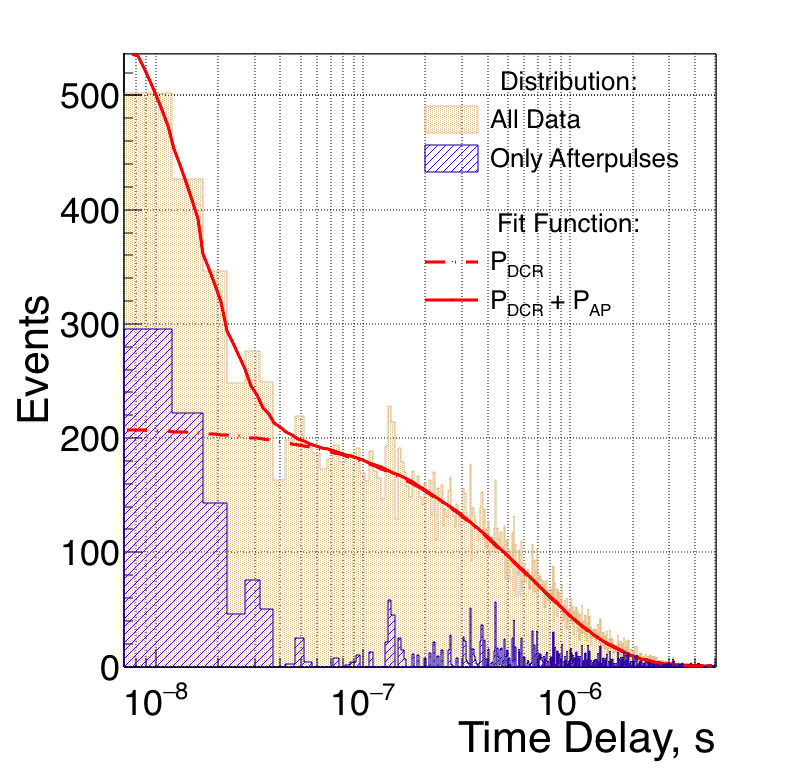
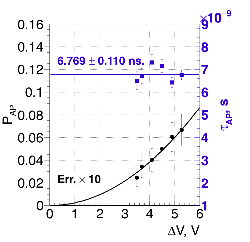
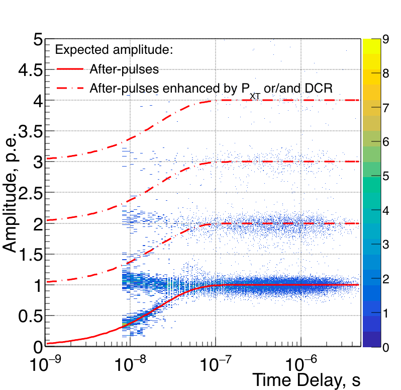
Fig. 20 is a two-dimensional histogram of the amplitude in p.e. of the first pulse following a primary pulse of 1 p.e. vs the time difference between the two. This plot shows the various SiPM noise components. The population of dots around amplitude of 1 p.e and time delay larger than 50 ns are typically dark pulses and afterpulses. Nonetheless, for this device only dark counts contribute due to the short afterpulse time constant . The population with amplitude lower than 1 p.e. and delay smaller than 50 ns are afterpulses produced when the cell has not yet recovered. The population at time delay less 50 ns and amplitude 1 p.e. might be mostly delayed optical cross-talk, and some dark pulses or afterpulses related to avalanches happened more than 5 s before the primary avalanche. The other populations at larger amplitude than 1 p.e. are of similar nature than what described for 1 p.e. but further enhanced by optical cross-talk. In the plot, the red solid line is calculated from Eq. 17 and the dashed lines are enhanced by optical cross-talk.
5 Optical characterisation
The photon detection efficiency () is one of the most important parameters describing the sensitivity of a SiPM as a function of wavelength of the incident light and the applied over-voltage : , where is the quantum efficiency, is the Geiger probability, and the cell fill factor (the percentage of it that is sensitive to light). More details about each component can be found in the Ref. [28]. To study the , our experimental setup at IdeaSquare at CERN was used (see Fig. 21). In this Section, the methods used for both absolute (at a given ) and relative (-dependent) measurement are reported and corresponding results discussed at the end of the section.
5.1 Absolute PDE measurements with pulsed light
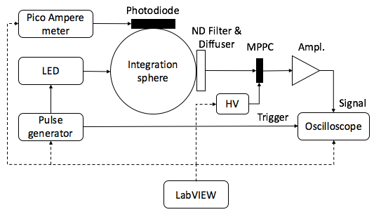
The schematic layout of the experimental set-up developed for absolute measurements is shown in Fig 21(a). The set-up is built around an integration sphere999Thorlab, Model IS200-4, used to produce at each output port a diffuse light of similar intensities by multiple scattering reflections on its internal surface. This destroys any spatial information of the incoming light usually produced by a LED but preserves the power at each port. A calibrated photodiode101010Hamamatsu S1337-1010BQ, s/n 61, placed on one output port, is used to determine the absolute amount of light scattered in the ports (power density), in order to estimate the number of photons impinging on the SiPM under test, sitting on the other port. The LED bias is provided by a pulse generator, with repetition rate of Hz, chosen to:
-
1.
have reasonable acquisition time ( min) for a full scan of the over-voltage in the range of 1 V 8 V with a step of 0.4 V, for each given wavelength;
-
2.
have a photocurrent level ( pA) at least 50 times higher than the SiPM dark photocurrent;
-
3.
not saturate the LED, which exhibits a non linear behaviour for kHz.
The dynamic range of the SiPM111111The dynamic range is the range where SiPM signal charge is linearly proportional to number of photons. As matter of fact, the SiPM linearity relies on the fact that each photon hits a different cell and the signal is the sum of the charge of the fired cells. If the density of photons is too high, the probability that a photon impinges on a cell, which has been already fired, and thus is inactive, becomes non negligible. In this case, not all photons contribute to the signal and then the linearity is lost and the device is said to be saturated. is much lower than the one of a generic photodiode. To be able to illuminate the SiPM with different light intensities, a Neutral Density Filter121212Thorlab, Model NE530B () is inserted between the integration sphere output port and the SiPM. To enable easy and fast replacement, the is mounted on a motorized wheel. To uniformly illuminate the SiPM full active area, a diffuser131313Thorlab, ED1-S50-MD is mounted after the . The surface uniformity is measured using a LED ( nm), and a small photodiode141414Thorlab, Model SM05PD2A (with 0.8 mm2 active area) mounted on a 2D translation stage151515two Thorlab LTS300 motorized stages connected together by Z-Axis bracket.. The light intensity non-uniformity, which has also to be taken into account for the calculation, was measured over the active area of the hexagonal SiPM and it is .
The power ratio, , between the light intensity measured by the calibrated photodiode, , and the SiPM, , is measured experimentally as described in Ref. [33]. Measurements were done for different light wavelengths (i.e. 405, 420, 470, 505, 530, 572 nm).
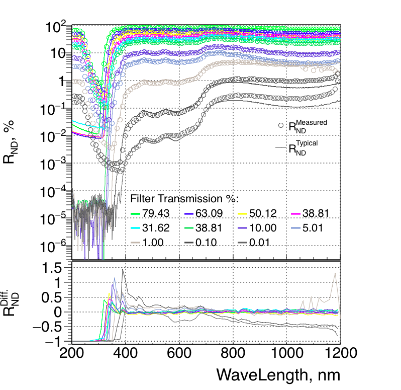
The transparency () of the at a given is measured as:
| (29) |
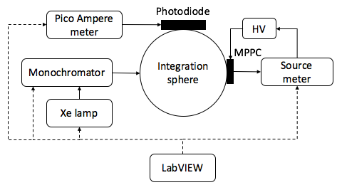
where is the number ( is used when there is no filter); and are the photocurrents measured by one photodiode positioned after the and the reference photodiode positioned at another output of the integration sphere, respectively; is the power ratio between the light intensity measured by the photodiodes when there is no . In order to measure , a Xenon lamp (75 W) was coupled with a monochromator161616Oriel Tunable Light Source System TLC-75X to select . The comparison between the measured values, , and the ”typical” one given by the producer, , as a function of and for different attenuation filters is presented in Fig. 22 together with the relative differences, on bottom of the figure.
The data acquisition system is similar to the one presented in Sec. 4.1. During data taking, the photocurrent of the photodiode is read out by the Keithley 6487. Data taking is triggered by a pulse generator and controlled by a Labview program to automate the necessary measurement steps.
The absolute is calculated using the so-called Poisson method [22, 34, 33, 28] from the average number of detected photons, corrected by factor to take into account the uncorrelated SiPM noise:
| (30) | |||||
where and are the number of waveforms with no SiPM signal within the regions preceding it and the total number of recorded waveforms, respectively.
The can be calculated as:
| (31) |
where is the average number of photons hitting the SiPM. The can be estimated from converting the photocurrent from the calibrated photodiode as:
| (32) |
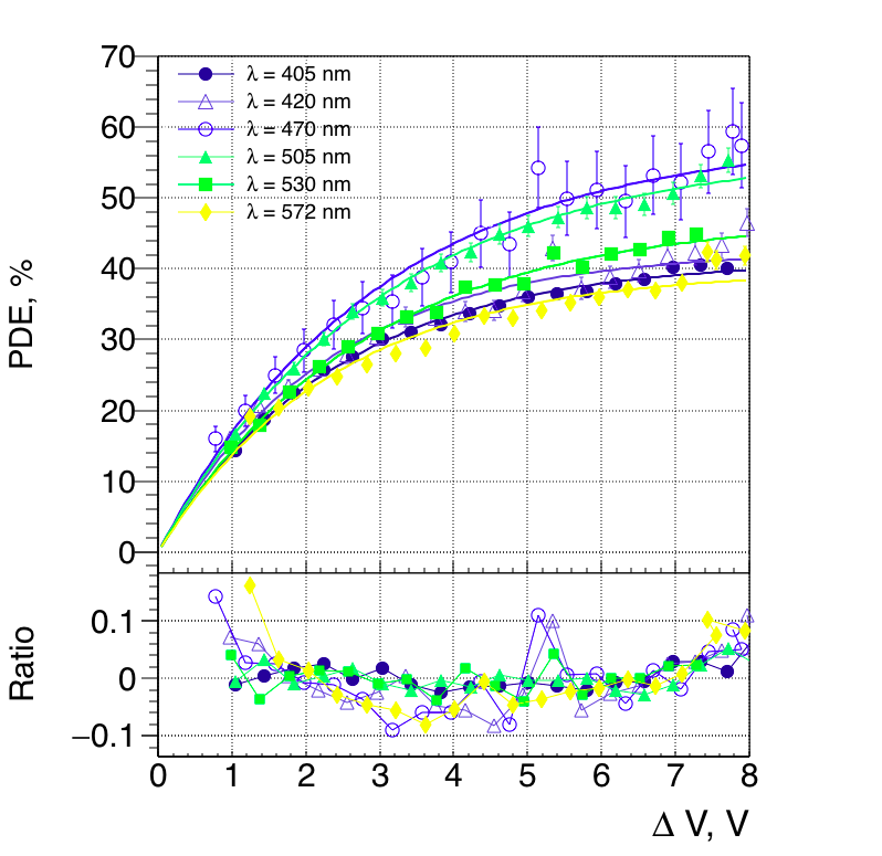
where is the photocurrent measured by the calibrated photodiode, is the photodiode quantum efficiency, is the pulse repetition frequency (typically ) and is the electron charge. The PDE as a function of for six different wavelengths is shown in Fig. 23. There are three main sources of uncertainty for the PDE determination:
-
1.
The precision on , calculated from the photodiode current, used for its calibration curve, and corrected by the power ratio .
-
2.
The determination of based on the separation of the “0 p.e.” and “1 p.e.” peaks, affected by SiPM noise (i.e. , and ), which are proportional to the .
-
3.
The precision of the calibrated quantum efficiency curve of the photodiode.
Therefore, for precise absolute measurements perfectly calibrated photodiodes, fast LEDs or lasers are strongly preferable. In the Fig. 23, we can observe that the error bars are different for different wavelengths. This reflects the variations of the LED light intensity during the measurements, which determine the precision of calculation.
The of a SiPM can be obtained fitting the data as a function of (see Fig. 23) for each wavelength with the function:
| (33) |
where is the Geiger probability (See. Eq. 12) and is a free parameter, which depends on SiPM type, light wavelength and to some extent on temperature [25]. Such a parameterisation provides a good description of our experimental data as shown in Fig. 23.
5.2 Relative PDE measurement with continuous light
The absolute measurements method requires a pulsed light source, as LEDs or a laser, so it is possible only for a limited number of wavelengths. Therefore, to measure the in a wide wavelength range, from 260 nm up to 1150 nm, a second method, the so called “Relative PDE”, is used. The schematic layout of the experimental set-up developed for the relative measurement is shown in Fig 21(b). The reverse current-voltage IV characteristics of the SiPM device at different wavelengths are performed using a Keithley 2400, while a Keithley 6487 is used to read photocurrent from calibrated photodiode.
The collection of reverse IV curves of the Hamamatsu S10943-2832(X) SiPM, for different wavelengths from 260 nm up to 1150 nm, is shown in Fig. 24. The difference between SiPM current with light and in dark condition at a given can be expressed as:
| (34) |
where is the at a given and , is the average number of photons sent to the SiPM device per given time interval, is the effective SiPM gain, namely the SiPM gain enhanced by cross-talk and afterpulses effects (for more details see Sec. 4.1). The is proportional to the photocurrent from the calibrated photodiode . Therefore, the relative in Eq. 34 can be rewritten as:
| (35) |
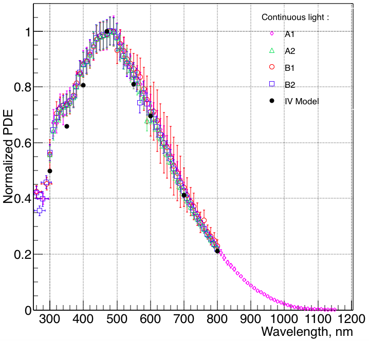
The relative as a function of at V is presented in Fig. 25, together with the values as calculated from the “IV Model” (see Sec. 3.2) by re-normalising them to the light intensity as estimated with the calibrated photodiode.
At a given temperature, the and of a SiPM device do not depend on light intensity, but only on the SiPM internal structure. Therefore, a simultaneous fit is done assuming that and are the same for all curves. To reduce computing time, the fit procedure used only eight curves corresponding to 300, 350, 400, 470, 550, 600, 700 and 800 nm wavelengths. The relative calculated from the “IV Model” is in good agreement with the results calculated from Eq. 35, as shown in Fig. 25. The main advantage of the “IV Model” for relative calculation is that also the breakdown voltage is extracted from the fit. As a matter of fact, in Eq. 35 the currents are measured as function of and then to derive the vs over-voltage, the has to be known or determined independently.
To have an absolute vs , the relative is normalised to the absolute values obtained from Eq.33 at V and presented in Fig. 26. Due to the complicated behaviour of the vs , a sum of three polynomial functions is used to fit the experimental data from 260 up to 1000 nm:
where , with , and are free parameters and are Heaviside step functions in the ranges:
nm 370 nm,
nm 530 nm,
nm nm.
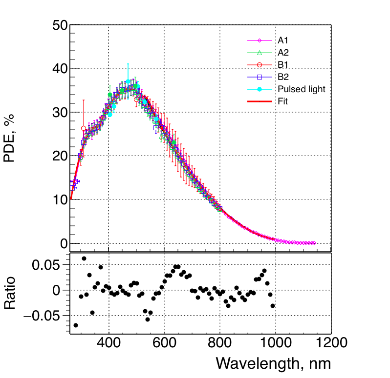
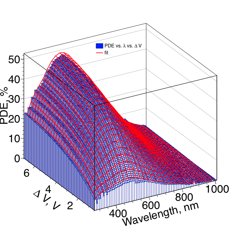
The as a function of and is particularly useful to predict its variations with experimental conditions, such as temperature or the NSB [35], which affects and then the sensor response. The as a function of and , shown in Fig. 27, can be obtained by combining the the absolute and relative measurements.
The analytical expression of the is given in Eq. 33. As can be seen in Fig. 28, data and this representation agree within 3% on average. At low over-voltages ( V), there is the largest disagreement between the fit function and the data:
-
1.
nm, the Xe lamp was operated with a larger slit width of 1.24 mm, to have enough light. As consequence, the wavelength resolution was of 16.1 nm and this resulted in lower precision on (See Fig. 26) and then in a worse quality fit;
-
2.
for nm, the photocurrent generated by the SiPM is comparable to its dark current (see Fig. 24) and, therefore, the signal to noise ratio is low.
5.3 Geiger probability
The Geiger probability , also known as triggering probability, represents the probability that a carrier reaching the high field region will trigger an avalanche.
The as a function of for different wavelengths is shown in Fig. 29, where it is evident how increases with increasing much rapidly for short wavelengths (blue light). Oldham [36] and McIntyre [23] relate this behaviour to the properties of light absorption in silicon and to the SiPM cell structure and ionisation rates of electrons, . and holes, . In particular, for -sub-structure at short wavelengths (blue light) is dominated by while at long one (red light) it is dominated by . Thus, the fast increase of with at short is related to the fact that [37].
The average probabilities that thermal pulses (see Sec. 4.5) or pulses created by optical cross-talk (see Sec. 4.5.1) trigger an avalanche are indicated as and in Fig. 29. As can be seen, is equal to (black dashed line) at = 565 nm and (red dashed line) is equal to at = 1041 nm. From this and previously discussed behavior between and , we may conclude that:
-
1.
the main contribution of is triggered by both electrons and holes;
-
2.
the main contribution of is triggered by holes;
6 Conclusions
In this work we report about the characterization measurements of the large area hexagonal SiPM S10943-2832(X). We measure all relevant SiPM parameters, detailed in Tab. 2. We also show how to build a PDE function of the wavelength and over-voltage. This is of paramount importance to determine the working point of SiPMs in real applications where external factors can affect its parameters, such as in the presence of NSB. Additionally, we compare several methods commonly used for estimate from the reverse current voltage measurement. The functions to fit , and are discussed. We also show how, from these fits, the triggering probability as function of the wavelength can be extracted. From its behaviour we infer that the DCR is triggered by both electrons and holes, while the cross-talk is initiated by avalanches triggered mainly by holes.
| Breakdown voltage | 54.699 0.017 0.025 V |
|---|---|
| (@) | 26.50 0.15 KHz |
| (@) | 1.735 0.04 KHz |
| (@) | 6.5 % |
| (@ within 5 s) | 2 % |
| PDE (@ = 472 nm ) | 35.5 3.5 % |
| Peak sensitivity wavelength | 480 nm |
| Quenching resistor | 182.9 0.3 31. |
Acknowledgements
This project has received funding from the European Unionfls Horizon 2020 research and innovation programme under grant agreement No 713171. Also, we acknowledge the support of the SNF funding agency. This paper has gone through internal review by the CTA Consortium.
References
References
-
[1]
Y. Sun, J. Maricic,
SiPMs
characterization and selection for the DUNE far detector photon detection
system, JINST 11 (01) (2016) C01078.
URL http://stacks.iop.org/1748-0221/11/i=01/a=C01078 -
[2]
H. Anderhub, et al.,
Design and
Operation of FACT – The First G-APD Cherenkov Telescope, JINST 8 (06)
(2013) P06008–P06008.
doi:10.1088/1748-0221/8/06/p06008.
URL https://doi.org/10.1088%2F1748-0221%2F8%2F06%2Fp06008 -
[3]
M. Heller, et al., An innovative silicon photomultiplier digitizing camera for gamma-ray
astronomy, The European Physical Journal C 77 (1) (2017) 47.
doi:10.1140/epjc/s10052-017-4609-z.
URL https://doi.org/10.1140/epjc/s10052-017-4609-z - [4] J. Aguilar, et al., Design, optimization and characterization of the light concentrators of the single-mirror small size telescopes of the Cherenkov Telescope Array, Astrop. Phys. 60 (2015) 32. doi:{10.1016/j.astropartphys.2014.05.010}.
-
[5]
J. Aguilar, et al.,
The front-end electronics and slow control of large area SiPM for the SST-1M
camera developed for the CTA experiment, Nucl. Instrum. Meth. A 830 (2016)
219 – 232.
doi:https://doi.org/10.1016/j.nima.2016.05.086.
URL http://www.sciencedirect.com/science/article/pii/S0168900216304788 -
[6]
Series
2400 sourcemeter line.
URL http://www.testequipmenthq.com/datasheets/KEITHLEY-2400-Datasheet.pdf - [7] W. Shockley, The Theory of p-n Junctions in Semiconductors and p-n junction Transistors, Bell System Technical Journal (1949) 435–489.
- [8] W. Shockley and W.T. Read, Statistics of the Recombinations of Holes and Electrons, Phys. Rev. 87 (1952) 835. doi:{10.1103/PhysRev.87.835}.
- [9] E. H. Hall, On a New Action of the Magnet on Electric Currents, American J. of Math. 2 (3) (1879) 287.
- [10] J. Frenkel, On Pre-Breakdown Phenomena in Insulators and Electronic Semi-Conductors, Phys. Rev. 54 (1938) 647. doi:10.1103/PhysRev.54.647.
- [11] Hamamatsu Photonics K.K.′Opto-semiconductor Handbook′ Editorial Committee, Opto-semiconductor Handbook, Hamamatsu Photonics K.K.Solid State Division (2014) 60–61.
- [12] E. Garutti, M. Ramilli, C. Xu, W. L. Hellweg, R. Klanner, Characterization and X-Ray Damage of Silicon Photomultipliers, PoS TIPP2014 (2014) 070. doi:10.22323/1.213.0070.
- [13] M. Simonetta, et al., Test and characterisation of SiPMs for the MEGII high resolution Timing Counter, Nucl. Instrum. Meth. A 824 (2016) 145. doi:10.1016/j.nima.2015.11.023.
- [14] N. Ferenc, G. Hegyesi, K. Kalinka and J. Molnár, A model based {DC} analysis of SiPM breakdown voltages, Nucl. Instrum. Meth. A 849 (2017) 55. doi:https://doi.org/10.1016/j.nima.2017.01.002.
- [15] N. Dinu, A. Nagai and A. Para, Breakdown voltage and triggering probability of SiPM from IVå curves at different temperatures, Nucl. Instrum. Meth. A 845 (2017) 64, Proc. of the Vienna Conf. on Instr. 2016. doi:https://doi.org/10.1016/j.nima.2016.05.110.
- [16] A. Nagai, N. Dinu, A. Para, Breakdown voltage and triggering probability of SiPM from IV curves, in: 2015 IEEE Nucl. Sci. Symp. and Med. Im. Conf., 2015, pp. 1–4. doi:10.1109/NSSMIC.2015.7581735.
- [17] G. Bonanno, D. Marano, M. Belluso, S. Billotta, A. Grillo, S. Garozzo, G. Romeo, M. C. Timpanaro, Characterization Measurements Methodology and Instrumental Set-Up Optimization for New SiPM Detectors Part I: Electrical Tests, IEEE Sensors Journal 14 (10) (2014) 3557–3566. doi:10.1109/JSEN.2014.2328621.
- [18] N. Serra et al., Experimental and TCAD Study of Breakdown Voltage Temperature Behavior in SiPMs, IEEE Trans. on Nucl. Sci. 58 (3) (2011) 1233. doi:{10.1109/TNS.2011.2123919}.
- [19] Z. Guoqing, H. Dejun, Z. Changjun and Z. Xuejun, Turn-on and turn-off voltages of an avalanche p n junction, J. of Semiconductors 33 (9) (2012) 094003.
-
[20]
V. Chmill, E. Garutti, R. Klanner, M. Nitschke, J. Schwandt,
On the characterisation of SiPMs from pulse-height spectra, Nucl. Instrum.
Meth. A 854 (2017) 70 – 81.
doi:https://doi.org/10.1016/j.nima.2017.02.049.
URL http://www.sciencedirect.com/science/article/pii/S0168900217302334 - [21] A. Nagai, N. Dinu-Jaeger, A. Para, Silicon Photomultiplier for Medical Imaging -Analysis of SiPM characteristics- (2019). arXiv:1907.03926.
-
[22]
P. Eckert, H.-C. Schultz-Coulon, W. Shen, R. Stamen, A. Tadday,
Characterisation studies of silicon photomultipliers, Nucl. Instrum. Meth.
A 620 (2) (2010) 217 – 226.
doi:https://doi.org/10.1016/j.nima.2010.03.169.
URL http://www.sciencedirect.com/science/article/pii/S0168900210008156 - [23] R. J. McIntyre, Theory of Microplasma Instability in Silicon, J. Appl. Phys. 32 (1961) 983.
-
[24]
A. N. Otte, D. Garcia, T. Nguyen, D. Purushotham,
Characterization of three high efficiency and blue sensitive silicon
photomultipliers, Nucl. Instrum. Meth. A 846 (2017) 106 – 125.
doi:https://doi.org/10.1016/j.nima.2016.09.053.
URL http://www.sciencedirect.com/science/article/pii/S0168900216309901 -
[25]
G. Collazuol, M. Bisogni, S. Marcatili, C. Piemonte, A. D. Guerra,
Studies of silicon photomultipliers at cryogenic temperatures, Nucl.
Instrum. Meth. A 628 (1) (2011) 389 – 392, VCI 2010.
doi:https://doi.org/10.1016/j.nima.2010.07.008.
URL http://www.sciencedirect.com/science/article/pii/S0168900210015500 -
[26]
J. Bude, N. Sano, A. Yoshii,
Hot-carrier
luminescence in Si, Phys. Rev. B 45 (1992) 5848–5856.
doi:10.1103/PhysRevB.45.5848.
URL https://link.aps.org/doi/10.1103/PhysRevB.45.5848 -
[27]
C. Piemonte, A. Gola,
Overview on the main parameters and technology of modern Silicon
Photomultipliers, Nucl. Instrum. Meth. A 926 (2019) 2 – 15, silicon
Photomultipliers: Technology, Characterisation and Applications.
doi:https://doi.org/10.1016/j.nima.2018.11.119.
URL http://www.sciencedirect.com/science/article/pii/S0168900218317716 -
[28]
F. Acerbi, S. Gundacker,
Understanding and simulating SiPMs, Nucl. Instrum. Meth. A 926 (2019) 16 –
35, silicon Photomultipliers: Technology, Characterisation and Applications.
doi:https://doi.org/10.1016/j.nima.2018.11.118.
URL http://www.sciencedirect.com/science/article/pii/S0168900218317704 - [29] J. A. Grieve, R. Chandrasekara, Z. Tang, A. Ling, Correcting for accidental correlations in saturated avalanche photodiodes, Opt. Express 24 (2016) 3592–3600. arXiv:1509.03959, doi:10.1364/OE.24.003592.
-
[30]
A. Nagai, et al.,
SENSE: A comparison of photon detection efficiency and optical crosstalk of
various SiPM devices, Nucl. Instrum. Meth. A 912 (2018) 182 – 185, new
Developments In Photodetection 2017.
doi:https://doi.org/10.1016/j.nima.2017.11.018.
URL http://www.sciencedirect.com/science/article/pii/S0168900217312044 - [31] A.L. Lacaita et al., On the bremsstrahlung origin of hot-carrier-induced photons in silicon devices, IEEE Trans. on Elect. Devices 40 (1993) 577. doi:10.1109/16.199363.
- [32] N. Dinu, et al., Temperature and bias voltage dependence of the MPPC detectors, in: IEEE Nucl. Sci. Symp. and Med. Im. Conf., 2010, pp. 215–219. doi:10.1109/NSSMIC.2010.5873750.
- [33] A. Basili, J.A. Aguilar, A. Christov, D. della Volpe, T. Montaruli, M. Rameez, Characterization of New Hexagonal Large Area MPPCs, IEEE Trans. on Nucl. Sci. 61 (2014) 1474. doi:{10.1109/TNS.2014.2321339}.
- [34] V. Chaumat, C. Bazin, N. Dinu, V. Puill, J.-F. Vagnucci, Absolute photo detection efficiency measurement of silicon photomultipliers, in: Proceedings of Science, 2012.
-
[35]
J. Aguilar, et al., Front-end
and slow control electronics for large area SiPMs used for the single mirror
Small Size Telescope (SST-1M) of the Cherenkov Telescope Array (CTA),
Proc.SPIE 9915 (2016) 9915 – 9915 – 8.
doi:10.1117/12.2232982.
URL http://dx.doi.org/10.1117/12.2232982 - [36] W. G. Oldham, R.R. Samuelson, P. Antognetti , Triggering Phenomenain Avalanche Diodes, IEEE Trans. on Elect. Devices 19 (1972) 1056–1060.
- [37] C. R. Crowell, S. M. Sze, Temperature Dependence of Avalanche Multiplication in Semiconductors, Applied Physics Letters 9 (1966) 242–244. doi:10.1063/1.1754731.