Dielectric constant of monolayer transition metal dichalcogenides across excitonic resonances
Abstract
We analyze the dielectric-function spectra of low dimensional transition metal dichalcogenides (TMDCs) using a fully analytical model of the complex dielectric function that is applicable in fractional dimensional space. We extract the dimensionalities of the and excitons as well as their Lorentzian broadening widths by fitting the model to experimental data in the spectral range of photon energies (1.5 - 3 eV). Our results show the significant contribution of the lowest ground exciton state to the dielectric properties of exemplary monolayer materials (MoS2, MoSe2 and WSe2). The exciton dimensionality parametrizes the processes that underlie confinement and many-body Coulomb effects as well as substrate screening effects, which simplifies the analysis of electro-optical properties in low dimensional systems. This study highlights the potential of theoretical models as valuable tools for interpreting the optical spectrum and in seeking an understanding of the correlated dynamics between the and excitons on the dielectric function of TMDCs.
I Introduction
The lattice dynamicsMolina-Sanchez and Wirtz (2011); Zhao et al. (2013); Cai et al. (2014); Zheng et al. (2017) and dielectric properties Park et al. (2018); Klots et al. (2018); Li et al. (2014a); Kumar and Ahluwalia (2012) of low dimensional transition metal dichalcogenides, MX2 (M = Mo, W, Nb and X = S, Se) are currently investigated with great interest for both theoretical studies Soh et al. (2018); Trushin et al. (2016); Trolle et al. (2017); Berkelbach et al. (2015); Kaasbjerg et al. (2012); Zhou et al. (2015); Mukherjee et al. (2015); Stroucken and Koch (2015); Trushin et al. (2016); Chakraborty et al. (2013); Steinhoff et al. (2016); Kolobov and Tominaga (2016); Chow et al. (2017), and high-performance device applications Woodward et al. (2015); Ou et al. (2014); Pospischil et al. (2014); Radisavljevic et al. (2011); Li et al. (2016); Fan et al. (2014); Perebeinos (2015); Beck et al. (2000); Tsai et al. (2013); Wi et al. (2014); Xu et al. (2015); Bertolazzi et al. (2013); Ji et al. (2013); Yu et al. (2016); Jariwala et al. (2017); Park et al. (2016); Feng et al. ; Woo et al. (2017). Excitons are confined strongly in low dimensional transition metal dichalcogenides (TMDCs) and display notable spectral features with desirable photoluminescence properties Splendiani et al. (2010); Plechinger et al. (2012); Ji et al. (2013); Zhu et al. (2016); Eda and Maier (2013); Berghäuser and Malic (2013); Molina-Sánchez et al. (2013); Mai et al. (2013); Gao et al. (2016); Ghatak et al. (2011). In Molybdenum disulfide (MoS2), a well known member of the TMDCs, there exist two pronounced peaks which are linked to the direct gap and excitons. These peaks arise due to the vertical transitions at the point from a spin-orbit split valence band to a doubly degenerate conduction band with decrease in the number of lattice layers Mak et al. (2010); Ramasubramaniam (2012); Cheiwchanchamnangij and Lambrecht (2012); Sim et al. (2013); Komsa and Krasheninnikov (2012); Qiu et al. (2013). Ultrafast optical pump-probe spectroscopic measurements display enhanced transient absorption blue-shifts for the and excitons in the monolayer MoS2 due to repulsive inter-excitonic interactions, with non-trivial linewidth broadening effects Sim et al. (2013).
The dielectric constant is an fundamental quantity that underpins experimental observables such as the refractive index and absorption coefficient Wemple and DiDomenico Jr (1971); Hopfield (1958); Takagahara (1993); Schmitt-Rink et al. (1989); Yoffe (2001); Tanguy et al. (1997) and provides valuable guidelines for the fabrication of optoelectronic and photonic devices. Due to reduced contributions from ionic and surface polarizabilities associated with one or cluster of atoms, the dielectric constant decreases with increase in the frequency of the electric field Hopfield (1958); Wemple and DiDomenico Jr (1971). Changes in the lattice structure that arise from frequency induced vibrations also contribute to an overall decrease of the polarization of the material. It is well known that the decreased dielectric screening and enhanced electron-electron correlation forces give rise to the high exciton binding energies noted in TMDCs Mak et al. (2010); Berghäuser and Malic (2013); Qiu et al. (2013); Cheiwchanchamnangij and Lambrecht (2012); Ross et al. (2013); Jones et al. (2013); Ramasubramaniam (2012); Thilagam (2014). Excitons are shown to dominate the dielectric properties of ultra-thin MoS2 of less than 5-7 layers Yu et al. (2015), with the dielectric function displaying an anomalous dependence on the layer number. Currently, there is lack of knowledge of the effect of the correlated dynamics between the and excitons Sim et al. (2013) on the dielectric function of TMDCs.
A comprehensive understanding of the role of excitons in the vicinity of the optical region provides useful guidelines in exploiting the dielectric properties of monolayer transition metal dichalcogenides for novel applications such as solar cells Pospischil et al. (2014); Tsai et al. (2014); Tsuboi et al. (2015); Liu et al. (2016); Thilagam (2016a), single-layer transistors Jariwala et al. (2013); Zhang et al. (2016) and light-emitting diodes Woodhead et al. (2016); Jeon et al. (2015); Clark et al. (2016). These reasons form the main motivation for this study where we employ the fractional dimension space approach (FDSA) Stillinger (2008); He (1991); Matos-Abiague et al. (1998); Christol et al. (1993); Mathieu et al. (1992); Lefebvre et al. (1993); Oh and Singh (1999); Reyes-Gómez et al. (2000); Thilagam (1997a, 1999); Lohe and Thilagam (2004) to examine the dielectric properties of the monolayer MoS2 and related common TMDCs. The FDSA maps an anisotropic quantum quasi-particle in real space to an isotropic environment parameterized by a single quantity () Stillinger (2008); He (1991); Matos-Abiague et al. (1998); Christol et al. (1993); Mathieu et al. (1992); Lefebvre et al. (1993) which may assume non-integer values. The parameter is independent of the physical mechanisms that are linked to confinement effects in TMDCs, which simplifies the evaluation of electro-optical properties in low dimensional systems Tanguy (1996); Tanguy et al. (1997). The theoretical predictions using FDSA yields good agreement with experimental findings Matos-Abiague et al. (1998); Christol et al. (1993); Mathieu et al. (1992); Thilagam (1997b), and provides qualitative insights that could be useful in the fabrication of devices. The FDSA enables understanding of the underlying quantum dynamical processes that control device operation, and provides valuable information on the cost effective fabrication of optical devices.
In this study, we compute the complex dielectric function of low dimensional transition metal dichalcogenides using a model of the exciton as a quasi-particle with arbitrary dimensions Tanguy (1996); Tanguy et al. (1997). In TMDCs, the exciton dimensionalities are known to vary between 1.7 and 2.5 Thilagam (2014) and may be quantified either by the ratio of the monolayer height to the exciton Bohr radius, or by the degree of confinement of the exciton within the monolayer plane. To this end, we analyze the contributions of the and excitons to the broadened complex dielectric constant based on the Kramers-Kronig relations. The calculations linked to these relations are simplified as the fractional dimensionalities and incorporate the blue-shifted absorption shifts and broadening effects arising from the quantum correlated dynamics between the and excitons Sim et al. (2013). A detailed analysis of the repulsive inter-excitonic interactions is beyond the scope of this study, however we aim to extract approximate estimates of the broadening effects of the and excitons using the FDSA formalism in this work.
II The dielectric constant of low-dimensional excitons
II.1 The dielectric constant in dimensions
The complex dielectric function that is applicable in dimensions reads as
| (1) | |||||
| (2) | |||||
| (3) |
where is the finite width of the Lorentzian broadened transitions and is the effective band gap of the bulk material that incorporates confinement effects.The symbol denotes the Euler gamma function, is the effective Rydberg and parametrizes the exciton oscillator strength. All bound and unbound states arising from Coulomb interactions are taken into account in Eq.1-3. Using Eq.1, we express the total dielectric function for the monolayer material via the Sellmeier equation and summing the contributions from the and excitons as
| (4) |
where and are the dielectric function contributions due to the and excitons respectively. The term quantifies the separation between the and excitonic peaks. The dimensions associated with the () exciton is denoted by (). The finite width of the Lorentzian broadened transitions associated with the () exciton is denoted by ().
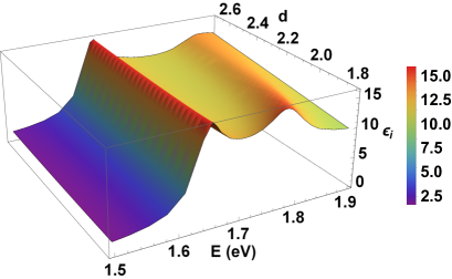
Fig.1 a, b illustrates the decrease of the imaginary component () of the exciton and corresponding increase of of the exciton with increase of the effective dimensions of both excitons ( and ). A decrease in the Lorentzian widths and results in sharper excitonic peaks as is to be expected. All other parameters used to generate Fig.1 a, b are listed below the figures. The strongly confined ground exciton state ( 2) contributes dominantly to the dielectric constant properties of the anisotropic material system as seen in Eqs.1 and 4. The contribution from the higher bound excitons states is significantly less as the oscillator strengths of the transitions (, ) are substantially decreased in higher order exciton states.

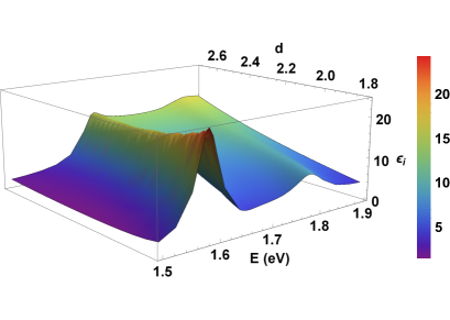
(b) Imaginary component of the dielectric constant using Eq.4 as a function of energy and the equal exciton dimensionalities = = . All other parameters used are the same as specified in (a) with the exception of = 0.025 eV, = 0.04 eV.
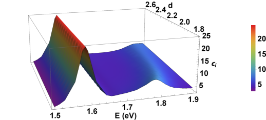
(b) Imaginary component of the dielectric constant using Eq.4 as a function of energy and the exciton dimensions = d with fixed = 2.5. All other parameters used are the same as specified in (a) above.
Fig. 2 a, b highlights the links between the dimensionality of the exciton, the dielectric constant as well as dimensionality of the exciton. The dimension of the exciton is fixed at = 1.8 in Fig.2 a, and at the higher = 2.5 in Fig.2 b. A gradual decrease in the imaginary component () of the exciton occurs with increase of its effective dimensionality. The results show that a lower exciton dimension = 1.8 is associated with a weakened contribution to the dielectric constant estimates by the exciton. There is partial qualitative agreement of these results with experimental observations Sim et al. (2013) of correlated interactions between the and excitons which are closely linked in momentum and energy space.
The complex spectral optical properties of low dimensional material systems are influenced by collision-induced excitonic linewidth broadening effects. The non-local quantum interaction between the and excitons is expected to influence the optical properties of highly confined material systems. A previous work has shown that the broadened exciton linewidth is linked to a diminished peak spectral amplitude of the exciton Sim et al. (2013). To this end, there is possibility that collision-induced excitonic linewidth broadening effects occurring at one exciton ( or ) may influence the spectral amplitude of the adjacent exciton. The incorporation of non-local quantum interactions between the and excitons as carried out in an earlier workThilagam (2010) is expected to introduce greater accuracy in the analysis of the mutually driven quantum correlated interactions between the and excitons.
II.2 The and excitonic peaks in monolayer MoS2
The dielectric function of the monolayer MoS2 displays three peaks that range from low to high energies and are labelled as Komsa and Krasheninnikov (2012). The and excitonic peaks arise from the electron-hole interaction between the spin-orbit split valence bands and the lowest conduction band at the and points. The () exciton is formed from the spin-up (spin-down) electrons in the conduction band (K-point of the BZ) and spin-down (spin-up) holes in the valence bands. The and excitons in general have almost similar behaviors, with any difference expected to arise from the position of holes in separate valence bands. The peak is linked to electron-hole interaction between the valence band and the conduction band in the vicinity of the and points Qiu et al. (2013). Ellipsometry optical techniques which allow the precise extraction of the dielectric function reveal the presence of the and exciton in the monolayer MoS2 on SiO2/Si substrates at 1.88 eV and 2.02 eV respectively Li et al. (2014b). There exist three contributing factors to the dielectric constant in this region: 1) the lowest bound exciton, 2) all other higher bound exciton states, and 3) continuum contribution that incorporates a Sommerfeld factor due to Coulomb attraction. The weak higher bound exciton states tend to merge with increase in number of states, hence the contribution from the lowest bound exciton is considered separately from the rest of the higher bound states. With increase in the exciton binding energies at lower dimensions, the resonance energies of the monolayer dielectric function are shifted from the corresponding energies in the bulk material Li et al. (2014a).
II.3 Comparison of theoretical results with experimental data: monolayer MoS2
The complex in-plane dielectric functions of four monolayer TMDCs (MoS2, MoSe2, WS2, and WSe2) Li et al. (2014a) have been derived using Kramers-Kronig constrained analysis of the reflectance spectra of the monolayers placed on fused silica substrates. Here we focus on the optical spectrum region (1.5 - 3 eV) Li et al. (2014a) in the vicinity of the and excitonic peaks for the Molybdenum based monolayer materials: MoS2 and MoSe2. We determine the dimensions of the and excitons ( and ) as best-fit parameters based on the experimental data of Li et. al. Li et al. (2014a) and the NonlinearModelFit option in the Mathematica package. The nonlinear model for this procedure is constructed using the fractional dimensional space dielectric model of Eq. 4. Other than the dimensions and , we also determine and which are the respective amplitudes the and exciton, and the finite widths of excitonic transitions and . The band gap and which is the separation between the and excitonic peaks are taken as free parameters.
Fig. 3 illustrates the fitting of the experimental results of the imaginary component of the dielectric constant Li et al. (2014a) for the monolayer MoS2 material using the fractional dimensional dielectric model of Eq. 4. The best-fit parameters are extracted using the NonlinearModelFit function of Mathematica, with the effective Rydberg fixed at a specific value. A range of values (40 to 60 meV) of for the bulk MoS2 Saigal et al. (2016) has been reported, and we thus fix at two possible values of 45 meV and 55 meV. Using = 55 meV, results of the fitting procedure give = 2.0, = 1.95, effective band gap = 2.11 eV, = 0.17 eV, amplitudes = 2.27 and = 8.65 (blue line). The Lorentzian broadening widths are obtained as = 34 meV ( exciton) and = 83 meV ( exciton). Using = 45 meV, results of the fitting procedure give = 2.0, = 1.95, effective band gap = 2.08 eV, = 0.17 eV, amplitudes = 3.78 and = 9.37 (red line). The Lorentzian broadening widths using = 45 meV are obtained as = 45 meV ( exciton) and = 77 meV ( exciton). The estimates for band gap and the energy difference between and excitonic peaks are in reasonable agreement with those obtained in an earlier work Ramasubramaniam (2012); Komsa and Krasheninnikov (2012). The results here confirm that the ground exciton and states ( 2) contribute dominantly to the dielectric constant properties of the monolayer MoS2 in the optical region (1.5 - 3 eV), with the exciton dimensionality playing a critical role in determining the dielectric properties of monolayer systems.
Using the hydrogenic binding energy relation
| (5) |
we estimate the binding energy of the exciton to be about 220 meV (using = 55 meV) and 180 meV ( = 45 meV). The exciton has binding energy of about 244 meV ( = 55 meV) and 200 meV ( = 45 meV), due to the higher hole mass of one of the spin-orbit split valence bands. These predicted results using Eq. 5 are substantially smaller than the binding energies ( 0.85 eV) obtained in earlier works Cheiwchanchamnangij and Lambrecht (2012); Ramasubramaniam (2012); Komsa and Krasheninnikov (2012). but in fair agreement with the well-converged first principle Bethe-Salpeter derived estimates (200 meV to 300 meV) by A. Molina-Sanchez et al. Molina-Sánchez et al. (2013), and also with those of Berghäuser et al Berghäuser and Malic (2014) who obtained binding energies of 455 (465 meV) for () excitons respectively The scaling relation between band gap and exciton binding energy of 2D systems Jiang et al. (2017) implies typical exciton binding energies of around 400 to 500 meV for the monolayer MoS2 on a silicon substrate. There is also some consistency of our results with the exciton binding energy of 0.3 eV computed using = 77 meV in Ref.Soh et al. (2018), and also with the photoluminescence excitation spectroscopy results of monolayer MoS2 on fused silica which provided an exciton binding energy of 0.44 eV Hill et al. (2015). In the case of the MoS2 monolayer in vacuumBerghäuser and Malic (2014), larger binding binding energies of 860 and 870 meV were obtained for the , excitons. Due to the screening effects induced by the substrate, the exciton binding energy is reduced which correlates with an increased exciton dimensionality.
For TMDC monolayers supported on SiO2 substrates, the photoluminescence linewidth is generally larger than 10 meV at low temperatures. Based on the fitting results, the Lorentzian broadening widths of = 34 meV (45 meV) ( exciton) and = 83 meV (77 meV) ( exciton) at = 55 meV (45 meV) are of the same order of the broadened width of 60 meV evaluated in an earlier work Molina-Sánchez et al. (2016) for the monolayer MoS2. The broadening kinetics associated with the () exciton are known to arise from several sources: exciton-optical phonon Molina-Sánchez et al. (2016); Dey et al. (2016); Thilagam (2016b), exciton-acoustic phonon interactions Molina-Sánchez et al. (2016); Thilagam (2016c), exciton-impurity scattering Ajayi et al. (2017) and, inter-excitonic scattering processes Sim et al. (2013); Cadiz et al. (2017). The larger broadened width of the exciton can be attributed to its origin at the second valence band with availability of increased recombination pathways Molina-Sánchez et al. (2016) compared to the exciton. The differences in hole energy and population densities between the two distinct valence bands linked to the and excitons also account for broadening width differences in and .

The red line is obtained using = 45 meV and the fitted parameters are: the exciton dimensions = 2.0 and = 1.95, effective band gap = 2.08 eV, = 0.17 eV, amplitudes = 3.78 and = 9.37 (red line). The Lorentzian broadening widths of = 45 meV ( exciton) and = 77 meV ( exciton).
II.4 Comparison of theoretical results with experimental data: monolayer MoSe2
In few-layer MoSe2, the indirect bandgap and direct bandgap are nearly degenerate unlike the MoS2 system Tongay et al. (2012). There exist subtle differences between the monolayers MoSe2 and MoS2 in terms of the reduced exciton mass, dielectric constants Kylänpää and Komsa (2015) and band gaps Tongay et al. (2012). Fig. 4 illustrates the fitting of the experimental results of the imaginary component of the dielectric constant Li et al. (2014a) for the monolayer MoSe2 with the fractional dimensional dielectric model of Eq. 4. By fixing the effective Rydberg at 50 meV, we get from the fitting procedure: = 2.05, = 1.98, effective band gap = 1.77 eV, = 0.24 eV, amplitudes = 1.5 and = 5.4 and the Lorentzian broadening widths of = 29 meV ( exciton) and = 82 meV ( exciton). Using Eq. 5 and the exciton dimensions obtained here, the binding energy of the exciton is evaluated as 181 meV and that of the exciton as 208 meV. With the effective Rydberg at 40 meV, we get the following results from the fitting procedure: = 2.01, = 1.98, effective band gap = 1.74 eV, = 0.22 eV, amplitudes = 2.3 and = 5.7 and the Lorentzian broadening widths of = 40 meV ( exciton) and = 70 meV ( exciton). Using Eq. 5 and the exciton dimensions obtained for = 40 meV, the binding energy of the exciton is evaluated as 160 meV and that of the exciton as 167 meV. The Lorentzian broadening widths of the exciton is larger than the exciton for reasons mentioned in the earlier section for the monolayer MoS2.

The red line is obtained using = 40 meV and the fitted parameters are: the exciton dimensions = 2.0 and = 1.98, effective band gap = 1.74 eV, = 0.22 eV, amplitudes = 2.30 and = 5.72 (red line). The Lorentzian broadening widths of = 40 meV ( exciton) d and = 70 meV ( exciton).
II.5 Comparison of theoretical results with experimental data: monolayer WSe2
The exciton binding energy in monolayers of tungsten diselenide (WSe2) has been determined via optical techniques to be 0.37 eV with a band gap energy of 2.02eV . Due to the strong spin-orbit coupling in WSe2, the energy separation between the and exciton is large (about 0.43 eV) He et al. (2014). Another study Hanbicki et al. (2015) revealed a much higher experimentally determined exciton binding energy of 0.79 eV showing the large variations in binding energies that exists amongst different experimental and theoretical groups. Experimental determination of the exciton binding energy of monolayer WSe2 was noted to be 240 meV on sapphire substrate while on gold the exciton binding decreased to 140 meV Park et al. (2018). As expected, the enhanced screening by the metal substrate results in lower binding and a larger dimensionality for the exciton.
Fig. 5 illustrates the fitting of the experimental results of the imaginary component of the dielectric constant Li et al. (2014a) for the monolayer WSe2 with the fractional dimensional dielectric model (see Eq. 4). Instead of using fixed estimates for the effective Rydberg , we allow the NonlinearModelFit function to yield appropriate values for . We obtain two possible estimates: = 42 meV and 52 meV and in both cases, we obtain slightly higher value for the dimensionality of the exciton compared to the exciton. The binding energies of the () exciton is about 231 meV (246 meV) for both values of the effective Rydberg. These binding energy estimates are comparable to that (240 meV) obtained on the insulator sapphire substrate by Part et. al. Park et al. (2018). The electronic band gap of 1.89 eV for the monolayer WSe2/sapphire substrate configuration Park et al. (2018) agrees well with the estimate of = 1.91 eV obtained using the NonlinearModelFit model in Fig. 5.
The large energy separation between the and exciton state of = 0.45 eV derived here is consistent with an earlier result (0.43 eV) He et al. (2014). We note that the Lorentzian broadening widths of = 117 meV ( exciton) is higher than the corresponding widths for the monolayer MoS2 and MoSe2 (see Table 1). The large broadened width of the WSe2 can be attributed to the enhanced recombination pathways at the location of the exciton due to its large energy separation from the exciton. It is likely that differences in hole population densities and exciton-phonon interactions between the two excitons further contribute to the wide variations seen in their Lorentzian broadening widths. Nevertheless further quantitative analysis is needed to identify the underlying factors that give rise to the wide difference in broadening widths between the and excitons. The theoretical fit around the region of the exciton as shown in Fig. 5 also indicates that further refinement is needed for the fractional dimensional model used in this study. This will be considered in future works.

The red line is obtained using parameters derived from the fitting procedure: = 52 meV , the exciton dimensions = 1.95 and = 1.92, effective band gap = 1.91 eV, = 0.45 eV, amplitudes = 1.12 and = 7.01 (red line). The Lorentzian broadening widths of = 24 meV ( exciton) and = 117 meV ( exciton).
Table 1 shows a comparison of the various best-fit parameters using imaginary component of the dielectric constant of the monolayer MoS2, MoSe2 and WSe2. The binding energies of the MoSe2 based excitons are lower than the binding energies of the monolayer MoS2, in agreement with earlier results Berkelbach et al. (2013); Komsa and Krasheninnikov (2012). The energy difference between the A and B transitions in the monolayer MoSe2 is larger than that in MoS2, consistent with the result of Li et al Li et al. (2014a) and Liu et al Liu et al. (2013). In comparison to the Molybdenum based monolayers, WSe2 displays a larger Lorentzian broadening width, .
III Conclusion
In summary, we have examined the dielectric properties of low dimensional transition metal dichalcogenides using a fractional dimensional space model of the complex dielectric constant expression. Such a model simplifies the analysis of electro-optical properties in monolayer systems, and enables easy comparison between the different monolayer TMDCs. Our results show that the ground exciton state ( 2) contributes strongly to the dielectric constant properties of the material system. For the monolayer materials (MoS2, MoSe2 and WSe2) examined here the oscillator strengths of the higher order exciton state transitions are substantially suppressed. For the purpose of rationalizing the excitonic features of different TMDCs, we extract the dimensionalities of the and excitons as well the broadening widths of excitonic transitions and using the theoretical model here and the experimental data of Li et. al. Li et al. (2014a) based on monolayers (MoS2, MoSe2, WSe2) placed on fused silica substrates. We also extract the band gap and the separation between the and excitonic peaks using the fractional dimensional space model and a NonlinearModelFit function, with the effective Rydberg fixed at a specific value in some cases.
There is good agreement between our theoretical predictions of the A-B splitting and the experimental results Li et al. (2014a) for the monolayer TMDCs (MoS2, MoSe2, and WSe2). The exciton binding energies agree reasonably well with exciton binding energy estimates obtained in earlier works Molina-Sánchez et al. (2013); Berghäuser and Malic (2014); Soh et al. (2018); Hill et al. (2015); Park et al. (2018). The results in this study show that the exciton has a marginally lower dimensionlity than the exciton in all the examined monolayer TMDCs. Moreover the non integer-dimensional occurrences of excitonic dimensionality presents as a reliable feature in computational modeling. The broadening width estimates of the and excitons (, ) derived using the fractional dimensional model reveal a larger width for the exciton which arises from differences in the environment of the two valence bands. The screening effects of the substrate influences the exciton dimensionality, and its binding energy. For instance, the the enhanced screening by a metal substrate results in a larger exciton dimensionality compared to a monolayer placed on an insulator substrate. Thus exciton dimensionalities can be controlled via the dielectric environment presented by the substrate.
The results in this study show that a lower exciton dimension is associated with a weakened contribution to the dielectric constant by the exciton. This is in qualitative agreement with experimental observations Sim et al. (2013) which show strong correlated inter-excitonic dynamics between the and excitons which are closely linked in momentum and energy space. Further understanding of the origin of the correlated dynamics between the and excitons and associated blue-shifted excitonic absorption could be useful for the design of quantum coupled optical devices. Lastly the fractional dimensional model of the complex dielectric function is useful in interpreting experimental data and for making predictions for properties of monolayer systems that are not accessible via current experimental techniques.
| System | (meV) | (eV) | (eV) | (meV) | (meV) | , | , Exciton binding (meV) | ||
|---|---|---|---|---|---|---|---|---|---|
| MoS2 | 55 | 2.0 | 1.95 | 0.17 | 2.11 | 34 | 83 | 2.27, 8.65 | 220, 244 (cf 200 to 300 Molina-Sánchez et al. (2013)) |
| MoS2 | 45 | 2.0 | 1.95 | 0.17 | 2.08 (1.90, 2.05 Mak et al. (2010)) | 45 | 77 | 3.78, 9.37 | 180, 200 (455, 465 Berghäuser and Malic (2014)) |
| MoSe2 | 50 | 2.05 | 1.98 | 0.24 | 1.77 | 28 | 82 | 1.50, 5.44 | 181, 208 |
| MoSe2 | 40 | 2.0 | 1.98 | 0.22 | 1.74 | 40 | 70 | 2.30, 5.72 | 160, 167 |
| WSe2 | 42∗ | 1.85 | 1.82 | 0.45 | 1.92 (cf 1.89 Park et al. (2018)) | 24 | 116 | 1.3, 8.51 | 231, 246 (cf 240 Park et al. (2018)) |
| WSe2 | 52∗ | 1.95 | 1.92 | 0.45 | 1.91 | 24 | 117 | 1.12, 7.01 | 231, 246 |
References
- Molina-Sanchez and Wirtz (2011) A. Molina-Sanchez and L. Wirtz, Physical Review B 84, 155413 (2011).
- Zhao et al. (2013) W. Zhao, Z. Ghorannevis, K. K. Amara, J. R. Pang, M. Toh, X. Zhang, C. Kloc, P. H. Tan, and G. Eda, Nanoscale 5, 9677 (2013).
- Cai et al. (2014) Y. Cai, J. Lan, G. Zhang, and Y.-W. Zhang, Physical Review B 89, 035438 (2014).
- Zheng et al. (2017) Q. Zheng, W. A. Saidi, Y. Xie, Z. Lan, O. V. Prezhdo, H. Petek, and J. Zhao, Nano Letters (2017).
- Li et al. (2014a) Y. Li, A. Chernikov, X. Zhang, A. Rigosi, H. M. Hill, A. M. van der Zande, D. A. Chenet, E.-M. Shih, J. Hone, and T. F. Heinz, Physical Review B 90, 205422 (2014a).
- Kumar and Ahluwalia (2012) A. Kumar and P. Ahluwalia, Physica B: Condensed Matter 407, 4627 (2012).
- Park et al. (2018) S. Park, N. Mutz, T. Schultz, S. Blumstengel, A. Han, A. Aljarb, L.-J. Li, E. J. List-Kratochvil, P. Amsalem, and N. Koch, 2D Materials 5, 025003 (2018).
- Klots et al. (2018) A. R. Klots, B. Weintrub, D. Prasai, D. Kidd, K. Varga, K. A. Velizhanin, and K. I. Bolotin, Scientific reports 8, 768 (2018).
- Trolle et al. (2017) M. L. Trolle, T. G. Pedersen, and V. Véniard, Scientific reports 7 (2017).
- Berkelbach et al. (2015) T. C. Berkelbach, M. S. Hybertsen, and D. R. Reichman, Physical Review B 92, 085413 (2015).
- Kaasbjerg et al. (2012) K. Kaasbjerg, K. S. Thygesen, and K. W. Jacobsen, Physical Review B 85, 115317 (2012).
- Zhou et al. (2015) J. Zhou, W.-Y. Shan, W. Yao, and D. Xiao, Physical review letters 115, 166803 (2015).
- Mukherjee et al. (2015) B. Mukherjee, F. Tseng, D. Gunlycke, K. K. Amara, G. Eda, and E. Simsek, Optical Materials Express 5, 447 (2015).
- Stroucken and Koch (2015) T. Stroucken and S. W. Koch, Journal of Physics: Condensed Matter 27, 345003 (2015).
- Trushin et al. (2016) M. Trushin, M. O. Goerbig, and W. Belzig, Physical Review B 94, 041301 (2016).
- Chakraborty et al. (2013) B. Chakraborty, H. Matte, A. Sood, and C. Rao, Journal of Raman Spectroscopy 44, 92 (2013).
- Steinhoff et al. (2016) A. Steinhoff, M. Florian, M. Rösner, M. Lorke, T. O. Wehling, C. Gies, and F. Jahnke, arXiv preprint arXiv:1603.03633 (2016).
- Kolobov and Tominaga (2016) A. V. Kolobov and J. Tominaga, in Two-Dimensional Transition-Metal Dichalcogenides (Springer, 2016) pp. 321–363.
- Chow et al. (2017) C. M. Chow, H. Yu, A. M. Jones, J. R. Schaibley, M. Koehler, D. G. Mandrus, R. Merlin, W. Yao, and X. Xu, arXiv preprint arXiv:1701.02770 (2017).
- Soh et al. (2018) D. B. Soh, C. Rogers, D. J. Gray, E. Chatterjee, and H. Mabuchi, Physical Review B 97, 165111 (2018).
- Woodward et al. (2015) R. Woodward, R. Howe, T. Runcorn, G. Hu, F. Torrisi, E. Kelleher, and T. Hasan, Optics express 23, 20051 (2015).
- Ou et al. (2014) J. Z. Ou, A. F. Chrimes, Y. Wang, S.-y. Tang, M. S. Strano, and K. Kalantar-zadeh, Nano letters 14, 857 (2014).
- Pospischil et al. (2014) A. Pospischil, M. M. Furchi, and T. Mueller, Nature nanotechnology 9, 257 (2014).
- Radisavljevic et al. (2011) B. Radisavljevic, M. B. Whitwick, and A. Kis, ACS nano 5, 9934 (2011).
- Li et al. (2016) S.-L. Li, K. Tsukagoshi, E. Orgiu, and P. Samorì, Chemical Society Reviews (2016).
- Fan et al. (2014) D. Fan, H. Liu, L. Cheng, P. Jiang, J. Shi, and X. Tang, Applied Physics Letters 105, 133113 (2014).
- Perebeinos (2015) V. Perebeinos, Nature nanotechnology 10, 485 (2015).
- Beck et al. (2000) A. Beck, J. Bednorz, C. Gerber, C. Rossel, and D. Widmer, Applied Physics Letters 77, 139 (2000).
- Tsai et al. (2013) D.-S. Tsai, K.-K. Liu, D.-H. Lien, M.-L. Tsai, C.-F. Kang, C.-A. Lin, L.-J. Li, and J.-H. He, Acs Nano 7, 3905 (2013).
- Wi et al. (2014) S. Wi, H. Kim, M. Chen, H. Nam, L. J. Guo, E. Meyhofer, and X. Liang, ACS nano 8, 5270 (2014).
- Xu et al. (2015) S. Xu, D. Li, and P. Wu, Advanced Functional Materials 25, 1127 (2015).
- Bertolazzi et al. (2013) S. Bertolazzi, D. Krasnozhon, and A. Kis, ACS nano 7, 3246 (2013).
- Ji et al. (2013) Q. Ji, Y. Zhang, T. Gao, Y. Zhang, D. Ma, M. Liu, Y. Chen, X. Qiao, P.-H. Tan, M. Kan, et al., Nano letters 13, 3870 (2013).
- Yu et al. (2016) C.-H. Yu, M.-L. Fan, K.-C. Yu, V. P.-H. Hu, P. Su, and C.-T. Chuang, IEEE Transactions on Electron Devices 63, 625 (2016).
- Jariwala et al. (2017) D. Jariwala, A. R. Davoyan, J. Wong, and H. A. Atwater, ACS Photonics (2017).
- Park et al. (2016) M. Park, Y. J. Park, X. Chen, Y.-K. Park, M.-S. Kim, and J.-H. Ahn, Advanced Materials (2016).
- (37) S. Feng, C. Cong, N. Peimyoo, Y. Chen, J. Shang, C. Zou, B. Cao, L. Wu, J. Zhang, M. Eginligil, et al., Nano Research , 1.
- Woo et al. (2017) M. H. Woo, B. C. Jang, J. Choi, K. J. Lee, G. H. Shin, H. Seong, S. G. Im, and S.-Y. Choi, Advanced Functional Materials (2017).
- Splendiani et al. (2010) A. Splendiani, L. Sun, Y. Zhang, T. Li, J. Kim, C.-Y. Chim, G. Galli, and F. Wang, Nano letters 10, 1271 (2010).
- Plechinger et al. (2012) G. Plechinger, F.-X. Schrettenbrunner, J. Eroms, D. Weiss, C. Schueller, and T. Korn, physica status solidi (RRL)-Rapid Research Letters 6, 126 (2012).
- Zhu et al. (2016) Y. Zhu, J. Yang, S. Zhang, S. Mokhtar, J. Pei, X. Wang, and Y. Lu, Nanotechnology 27, 135706 (2016).
- Eda and Maier (2013) G. Eda and S. A. Maier, Acs Nano 7, 5660 (2013).
- Berghäuser and Malic (2013) G. Berghäuser and E. Malic, arXiv preprint arXiv:1311.1045 (2013).
- Molina-Sánchez et al. (2013) A. Molina-Sánchez, D. Sangalli, K. Hummer, A. Marini, and L. Wirtz, Physical Review B 88, 045412 (2013).
- Mai et al. (2013) C. Mai, A. Barrette, Y. Yu, Y. G. Semenov, K. W. Kim, L. Cao, and K. Gundogdu, Nano letters 14, 202 (2013).
- Gao et al. (2016) W. Gao, Y. H. Lee, R. Jiang, J. Wang, T. Liu, and X. Y. Ling, Advanced Materials 28, 701 (2016).
- Ghatak et al. (2011) S. Ghatak, A. N. Pal, and A. Ghosh, Acs Nano 5, 7707 (2011).
- Mak et al. (2010) K. F. Mak, C. Lee, J. Hone, J. Shan, and T. F. Heinz, Physical Review Letters 105, 136805 (2010).
- Ramasubramaniam (2012) A. Ramasubramaniam, Physical Review B 86, 115409 (2012).
- Cheiwchanchamnangij and Lambrecht (2012) T. Cheiwchanchamnangij and W. R. Lambrecht, Physical Review B 85, 205302 (2012).
- Sim et al. (2013) S. Sim, J. Park, J.-G. Song, C. In, Y.-S. Lee, H. Kim, and H. Choi, Physical Review B 88, 075434 (2013).
- Komsa and Krasheninnikov (2012) H.-P. Komsa and A. V. Krasheninnikov, Physical Review B 86, 241201 (2012).
- Qiu et al. (2013) D. Y. Qiu, H. Felipe, and S. G. Louie, Physical review letters 111, 216805 (2013).
- Wemple and DiDomenico Jr (1971) S. Wemple and M. DiDomenico Jr, Physical Review B 3, 1338 (1971).
- Hopfield (1958) J. Hopfield, Physical Review 112, 1555 (1958).
- Takagahara (1993) T. Takagahara, Physical Review B 47, 4569 (1993).
- Schmitt-Rink et al. (1989) S. Schmitt-Rink, D. Chemla, and D. Miller, Advances in Physics 38, 89 (1989).
- Yoffe (2001) A. Yoffe, Advances in Physics 50, 1 (2001).
- Tanguy et al. (1997) C. Tanguy, P. Lefebvre, H. Mathieu, and R. Elliott, Journal of applied physics 82, 798 (1997).
- Ross et al. (2013) J. S. Ross, S. Wu, H. Yu, N. J. Ghimire, A. M. Jones, G. Aivazian, J. Yan, D. G. Mandrus, D. Xiao, W. Yao, et al., Nature communications 4, 1474 (2013).
- Jones et al. (2013) A. M. Jones, H. Yu, N. J. Ghimire, S. Wu, G. Aivazian, J. S. Ross, B. Zhao, J. Yan, D. G. Mandrus, D. Xiao, et al., Nature nanotechnology 8, 634 (2013).
- Thilagam (2014) A. Thilagam, Journal of Applied Physics 116, 053523 (2014).
- Yu et al. (2015) Y. Yu, Y. Yu, Y. Cai, W. Li, A. Gurarslan, H. Peelaers, D. E. Aspnes, C. G. Van de Walle, N. V. Nguyen, Y.-W. Zhang, et al., Scientific reports 5 (2015).
- Tsai et al. (2014) M.-L. Tsai, S.-H. Su, J.-K. Chang, D.-S. Tsai, C.-H. Chen, C.-I. Wu, L.-J. Li, L.-J. Chen, and J.-H. He, ACS nano 8, 8317 (2014).
- Tsuboi et al. (2015) Y. Tsuboi, F. Wang, D. Kozawa, K. Funahashi, S. Mouri, Y. Miyauchi, T. Takenobu, and K. Matsuda, Nanoscale 7, 14476 (2015).
- Liu et al. (2016) Y. Liu, W. Gao, and L. Hao, in Novel Optical Materials and Applications (Optical Society of America, 2016) pp. NoW1D–5.
- Thilagam (2016a) A. Thilagam, Journal of Mathematical Chemistry 55, 1 (2016a).
- Jariwala et al. (2013) D. Jariwala, V. K. Sangwan, D. J. Late, J. E. Johns, V. P. Dravid, T. J. Marks, L. J. Lauhon, and M. C. Hersam, Applied Physics Letters 102, 173107 (2013).
- Zhang et al. (2016) Q. Zhang, W. Bao, A. Gong, T. Gong, D. Ma, J. Wan, J. Dai, J. N. Munday, J.-H. He, L. Hu, et al., Nanoscale 8, 14237 (2016).
- Woodhead et al. (2016) C. S. Woodhead, J. Roberts, Y. J. Noori, Y. Cao, R. Bernardo-Gavito, P. Tovee, A. Kozikov, K. Novoselov, and R. J. Young, arXiv preprint arXiv:1607.05025 (2016).
- Jeon et al. (2015) P. J. Jeon, J. S. Kim, J. Y. Lim, Y. Cho, A. Pezeshki, H. S. Lee, S. Yu, S.-W. Min, and S. Im, ACS applied materials & interfaces 7, 22333 (2015).
- Clark et al. (2016) G. Clark, J. R. Schaibley, J. S. Ross, T. Taniguchi, K. Watanabe, J. R. Hendrickson, S. Mou, W. Yao, and X. Xu, Nano letters (2016).
- Stillinger (2008) F. H. Stillinger, Journal of Mathematical Physics 18, 1224 (2008).
- He (1991) X.-F. He, Physical Review B 43, 2063 (1991).
- Matos-Abiague et al. (1998) A. Matos-Abiague, L. Oliveira, and M. de Dios-Leyva, Physical Review B 58, 4072 (1998).
- Christol et al. (1993) P. Christol, P. Lefebvre, and H. Mathieu, Journal of applied physics 74, 5626 (1993).
- Mathieu et al. (1992) H. Mathieu, P. Lefebvre, and P. Christol, PHYSICAL REVIEW B 46 (1992).
- Lefebvre et al. (1993) P. Lefebvre, P. Christol, and H. Mathieu, Physical Review B 48, 17308 (1993).
- Oh and Singh (1999) I.-K. Oh and J. Singh, Physical Review B 60, 2528 (1999).
- Reyes-Gómez et al. (2000) E. Reyes-Gómez, A. Matos-Abiague, C. Perdomo-Leiva, M. de Dios-Leyva, and L. Oliveira, Physical Review B 61, 13104 (2000).
- Thilagam (1997a) A. Thilagam, Physical Review B 56, 4665 (1997a).
- Thilagam (1999) A. Thilagam, Physica B: Condensed Matter 262, 390 (1999).
- Lohe and Thilagam (2004) M. Lohe and A. Thilagam, Journal of Physics A: Mathematical and General 38, 461 (2004).
- Tanguy (1996) C. Tanguy, Solid state communications 98, 65 (1996).
- Thilagam (1997b) A. Thilagam, Physical Review B 56, 9798 (1997b).
- Thilagam (2010) A. Thilagam, Journal of Physics A: Mathematical and Theoretical 43, 155301 (2010).
- Li et al. (2014b) W. Li, A. G. Birdwell, M. Amani, R. A. Burke, X. Ling, Y.-H. Lee, X. Liang, L. Peng, C. A. Richter, J. Kong, et al., Physical Review B 90, 195434 (2014b).
- Saigal et al. (2016) N. Saigal, V. Sugunakar, and S. Ghosh, Applied Physics Letters 108, 132105 (2016).
- Berghäuser and Malic (2014) G. Berghäuser and E. Malic, Physical Review B 89, 125309 (2014).
- Jiang et al. (2017) Z. Jiang, Z. Liu, Y. Li, and W. Duan, Physical Review Letters 118, 266401 (2017).
- Hill et al. (2015) H. M. Hill, A. F. Rigosi, C. Roquelet, A. Chernikov, T. C. Berkelbach, D. R. Reichman, M. S. Hybertsen, L. E. Brus, and T. F. Heinz, Nano letters 15, 2992 (2015).
- Molina-Sánchez et al. (2016) A. Molina-Sánchez, M. Palummo, A. Marini, and L. Wirtz, Physical Review B 93, 155435 (2016).
- Dey et al. (2016) P. Dey, J. Paul, Z. Wang, C. Stevens, C. Liu, A. Romero, J. Shan, D. Hilton, and D. Karaiskaj, Physical review letters 116, 127402 (2016).
- Thilagam (2016b) A. Thilagam, Journal of Applied Physics 120, 124306 (2016b).
- Thilagam (2016c) A. Thilagam, Journal of Applied Physics 119, 164306 (2016c).
- Ajayi et al. (2017) O. A. Ajayi, J. V. Ardelean, G. D. Shepard, J. Wang, A. Antony, T. Taniguchi, K. Watanabe, T. F. Heinz, S. Strauf, X. Zhu, et al., 2D Materials 4, 031011 (2017).
- Cadiz et al. (2017) F. Cadiz, E. Courtade, C. Robert, G. Wang, Y. Shen, H. Cai, T. Taniguchi, K. Watanabe, H. Carrere, D. Lagarde, et al., Physical Review X 7, 021026 (2017).
- Tongay et al. (2012) S. Tongay, J. Zhou, C. Ataca, K. Lo, T. S. Matthews, J. Li, J. C. Grossman, and J. Wu, Nano letters 12, 5576 (2012).
- Kylänpää and Komsa (2015) I. Kylänpää and H.-P. Komsa, Physical Review B 92, 205418 (2015).
- He et al. (2014) K. He, N. Kumar, L. Zhao, Z. Wang, K. F. Mak, H. Zhao, and J. Shan, Physical review letters 113, 026803 (2014).
- Hanbicki et al. (2015) A. Hanbicki, M. Currie, G. Kioseoglou, A. Friedman, and B. Jonker, Solid State Communications 203, 16 (2015).
- Berkelbach et al. (2013) T. C. Berkelbach, M. S. Hybertsen, and D. R. Reichman, Physical Review B 88, 045318 (2013).
- Liu et al. (2013) G.-B. Liu, W.-Y. Shan, Y. Yao, W. Yao, and D. Xiao, Physical Review B 88, 085433 (2013).