Low temperature properties of whispering gallery modes in isotopically pure silicon-28
Abstract
Whispering Gallery (WG) mode resonators have been machined from a boule of single-crystal isotopically pure silicon-28. Before machining, the as-grown rod was measured in a cavity, with the best Bragg confined modes exhibiting microwave -factors on the order of a million for frequencies between 10 and 15 GHz. After machining the rod into smaller cylindrical WG mode resonators, the frequencies of the fundamental mode families were used to determine the relative permittivity of the material to be near 4 K, with the precision limited only by the dimensional accuracy of the resonator. However, the machining degraded the -factors to below . Raman spectroscopy was used to optimize post-machining surface treatments to restore high -factors. This is an enabling step for the use of such resonators for hybrid quantum systems and frequency conversion applications, as silicon-28 also has very low phonon losses, can host very narrow linewidth spin ensembles and is a material commonly used in optical applications.
I Introduction
In this work we describe investigations of the microwave properties of isotopically purified silicon-28 (28Si). The dielectric properties of the material are close to that of naturally occurring silicon, which is the primary material used in the manufacturing of semiconductor devices. Standard silicon is a mixture of silicon atoms consisting of 28, 29 and 30 nucleons with approximately , and abundance in nature, respectively. Of these isotopes, only 28Si and 30Si have zero nuclear spin. This feature means that pure crystals of these isotopes act as a so-called ‘virtual vacuum’ with respect to a bath of magnetic Two Level Systems (TLS), leaving the medium inert Wolfowicz et al. (2013), which is not true for standard silicon. Thus, the absence of nuclear spin in the lattice circumvents one of the most important channels of decoherence, leaving only phonon dissipation which can be greatly reduced through cooling.
As a result of the lack of nuclear spin, enriched 28Si has been demonstrated to be an ideal host material for solid-state qubits. Electron or nuclear spins of low-concentration impurities in bulk 28Si can form extremely well isolated quantum systems. These systems have been shown to exhibit coherence times () of up to seconds for the electron spin Tyryshkin et al. (2011), and minutes for the nuclear spin Steger (2012), which are comparable to those of qubits based on trapped ions Haljan (2005); Langer (2005). In addition, isotopically purified silicon has the potential to allow the development of a solid-state clock formed from an ensemble of impurity donorsSaeedi et al. (2015), a scheme which has also been proposed for other solid-state mediumsJin et al. (2015); Hodges et al. (2013); Goryachev et al. (2018). The measurement of clock transitions may make use of a microwave resonant cavity. If the silicon crystal itself acted as the microwave resonant cavity, utilising a particularly low-loss resonant family of modes - whispering gallery (WG) modes, the frequency stability and interaction strengths (and hence coherence times) could be vastly improved in these clock transitions. Furthermore, by manufacturing these resonators from enriched silicon, dephasing as a result of nuclear spin interaction could be removed.
Previously, a very low-loss paramagnetic spin ensemble was detected in enriched silicon with a narrow linewidth of less than 7 kHz for a 10 parts per trillion concentration of impurity ionsKostylev et al. (2017). This was only possible by virtue of the low dielectric photonic losses combined with the long lifetime of the spin transition (low magnetic loss), which enhanced the AC magnetic susceptibility. These results indicate that single crystal 28Si has immense potential for future cavity QED experiments and presents as an excellent candidate for a solid-state clock if impurities that exhibit clock transitions could be purposefully doped within the crystal.

In this work we present an analysis of WG mode measurements in an enriched silicon resonator. We characterise the modes and their losses, and discuss the manufacturing and treatment techniques that have been used to improve them.
II Preparation of isotopically pure whispering gallery mode resonators
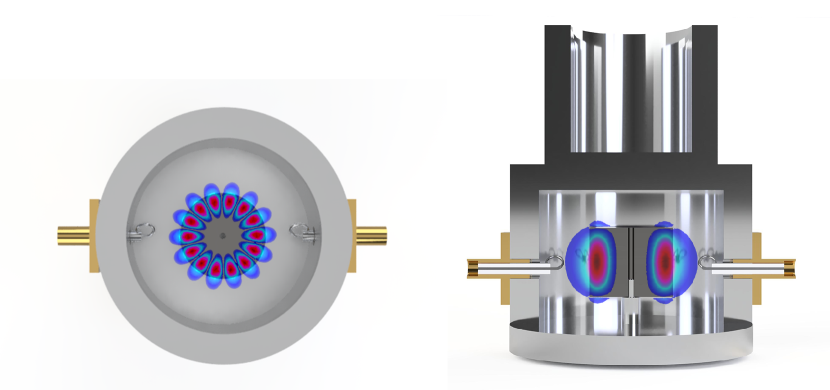
A crystal boule approximately mm diameter and mm length was grown using the float zone melting method in an argon atmosphereItoh et al. (2003) at the G.G. Devyatykh Institute of Chemistry of High-Purity Substances. The specified concentration of 28Si was , with concentration of oxygen and carbon estimated to be less than cm-3 (on the order of 1 ppm) and boron and phosphorous to be less than cm-3 (on the order of 1 ppb). The boule as-drawn from the melt is cylindrical, with a radius that can clearly be seen to vary by visual inspection. Thus, initial predictions of mode frequencies in the boule were imprecise, making it difficult to properly characterize any photon-spin interactions. To solve this problem, the boule was machined to make four smaller, more dimensionally precise cylindrical resonators. The crystal was turned to have a uniform cylindrical diameter, which was measured to be mm. This rod was then diced into four equal cylinders of 14.90 mm height, which were optically polished on the end faces and drilled through the axial centre of the crystal to a diameter of 1 mm. A photo of the as-grown rod along with three of the diced cylindrical resonators is shown in Fig. 1. Two cavities to house the WG mode resonators for characterization were then machined from oxygen-free copper and aluminium, each with an integrated support post. A schematic of the resonator loaded cavity is shown in Fig. 2.
III Characterization of isotopically pure whispering gallery mode resonators
The cylindrical WG mode resonators support quasi-Transverse Electric (WGE) and quasi-Transverse Magnetic (WGH) modes. To allow accurate prediction of these mode frequencies, precise measurements of all dimensions of the cavity and resonator were first made at room temperature. We then calculated the dimensional change at cryogenic temperatures using published values for the coefficient of thermal expansion for all materials. The resulting dimensions were used to define a model in finite element analysis software (COMSOL Multiphysics), in which we implemented an ultra-fine mesh that reduced frequency errors to below that of the dimensional errors of the WG mode cavity. An example of the computed field density for the WGH7,1,1 mode at GHz is shown in Fig. 2, overlayed on top of a 3D rendering of the crystal and housing. Initial simulations were performed using the low temperature permittivity value for standard float-zone silicon at microwave frequencies published previouslyKrupka et al. (2006). That value, , was calculated from the frequencies of higher order TE0,x modes.
For measurement, the resonator loaded cavity was placed under vacuum and cooled to as low as 20 mK with a dilution refrigerator. The experimental setup was similar to that used previously for investigations of other materials at low temperatureFarr et al. (2013); Goryachev et al. (2013, 2015). In this setup, the incident microwave signal was attenuated to the level of a few photons by a chain of room temperature and cold attenuators, and the output signal was amplified by a series of cold high-electron-mobility transistor (HEMT) and room temperature amplifiers. These signals were coupled to the resonator using diagonal loop probes to permit coupling to both transverse and axial fields, and hence to both WGH and WGE families.

To further refine the model, a large number of resonant modes were measured with a vector network analyzer, and identified by comparison with the frequencies calculated in COMSOL. The highest -factor modes were exhibited by the fundamental WG mode families, which allowed easy identification. The frequency and -factors of the candidate modes will be discussed further below. The frequency discrepancy between measured and calculated values allowed us to determine more precisely the permittivity of our sample. For WG modes, most of the field is confined within the dielectric crystal, which greatly suppresses perturbations due to the metal support post and cavity walls. Correspondingly, the whispering gallery mode technique has been shown previously to be the most accurate for characterizing low-loss crystalsKrupka et al. (1999). By comparing the four highest frequency WGEm,1,1 and WGHm,1,1 modes (as shown in Table 1) we determine the permittivity to be . This is the mean value of permittivity which results in a perfect match between simulation and experiment for the four modes, with the error defined as twice the standard error. This shows excellent relative precision, however, our precision in the dimensions of the cavity are actually much worse, and taking this into account results in a value of . Using this value, experiment and simulation are compared in Table 1 and displayed graphically in Fig. 3.
| Mode | Calculated (GHz) | Measured (GHz) |
|---|---|---|
| WGH7,1,1 | 19.5350 | |
| WGE6,1,1 | 19.4160 | |
| WGH6,1,1 | 17.3010 | |
| WGE5,1,1 | 17.1840 |

IV Characterization and repair of surface strain
The process of machining the resonators into uniform cylinders resulted in a significant degradation of the microwave -factors achievable in the sample. To investigate the effect of damage introduced by the lathe turning process, the surfaces of the samples were analysed using Raman spectroscopy with results shown in Fig. 4. Raman spectra were acquired by focusing the 532 nm line of a frequency doubled Nd:YAG laser onto the surface of the resonator with a confocal microscope. A 100 objective lens with a numerical aperture of 0.9 resulting in a 1 m laser spot size was used, with the laser power set to 15 mW (as measured before the objective) for all measurements. Spectra were collected for 10 seconds with a Renishaw InVia Reflex 0.25 working distance micro-Raman spectrometer with a 2400 grooves/mm grating. The overall wave number error was estimated to be 0.5 cm-1. The spectral resolution of the setup was 1.1 cm-1 per CCD pixel for the 2400 mm-1 grating.
Crystalline silicon has a characteristic Raman peak at 520 cm-1 corresponding to inelastic scattering from the triply degenerate first-order optical phonon modes of silicon (one longitudinal and two transverse optic phonons). Strain or crystal imperfections can introduce linewidth broadening or shifting of this Raman peak. Upon examination, the end faces which were optically polished showed no such signs of surface strain, with the spectra in several locations nominally identical to that of a calibration sample of (natural abundance) silicon. However, the cylindrical side faces of the resonator exhibited strong variation in the Raman spectrum at several locations, indicating localised strain damage (Fig. 4(a)). This type of surface damage is known to introduce microwave losses Taber and Flory (1995); Braginsky et al. (1987), and is a likely cause of the low -factor values shown in grey in Fig. 5.
To repair the surface damage introduced by machining, a cleaning, acid etching, and annealing procedure was carried out. The 28Si resonator was first cleaned by sonication in acetone, isopropyl alcohol and de-ionised water for 10 minutes each. This was followed by 10 minute clean in Piranha solution (H2SO4(70%) and H2O2(30%) in a 4:1 ratio) and RCA solution (H2O, H2O2(30%), and HCl(30%) in a 5:1:1 ratio) for 10 minutes. The resonator was then submerged in a 5% solution of hydrofluoric acid in deionised water for 20 seconds, and rinsed with deionised water.
An anneal was then performed to relieve surface strain and damage, but additionally to reduce the density of paramagnetic centres on the silicon surface which may lead to increased microwave losses. This was achieved by annealing in oxygen for 1 hour at 1000∘C, followed by a 1 hour anneal in nitrogen to ensure a low fixed oxide charge density in the surface oxide. A forming gas anneal (5% H in Ar) at 450∘C for 30 minutes was then used to passivate dangling bonds at the Si/SiO2 interface. The density of states at the surface is estimated to be in the low 1010 cm-2/eV for the Si-SiO2 interface as determined with electrical measurements of a test sample.
After undergoing these treatments, Raman spectra taken at several locations on the crystal indicated repair of surface strain, with no broadening or shifting of the characteristic Raman peak observed (Fig. 4(b)). The background corrected Raman data are well modelled using a Voigt function. Fits to the spectra from the as-machined surface had a mean Raman shift of cm-1 (standard deviation cm-1), with a mean FWHM linewidth of cm-1 ( cm-1), compared to a mean Raman shift of cm-1 ( cm-1) and FWHM cm-1 ( cm-1) for the top surfaces. Such a shift is equivalent to a uniaxial strain of over 0.5 GPa.De Wolf et al. (1996) After the acid treatment and annealing, the Raman data shows good recovery of the crystal, with mean Raman shift cm-1 ( cm-1), and FWHM cm-1 ( cm-1).
V Measurement after surface repair

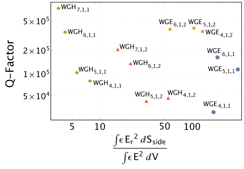
After processing to relieve surface strain and passivate dangling bonds, the 28Si resonator was placed in an aluminium cavity for cryogenic measurement. Aluminium becomes superconducting below 1.2 K, and thus was used in order to reduce microwave losses in the cavity walls when cooled to millikelvin temperature. In this way, the intrinsic -factor of the crystal can be determined with the highest accuracy, with minimal influence from other sources of loss such as resistive dissipation in the cavity walls. The measured -factors before (grey points) and after treatment (coloured points) are plotted in Fig. 5.
The results show that the -factors after treatment have been restored close to the high values prior to machining Kostylev et al. (2017). The results indicate that the maximum -factor was not fully reached given the data in Fig. 5 appears as though -factors would continue increasing for higher frequency modes.
Included in Fig. 5 are the limits on -factors imposed by potential loss mechanisms. The total -factor of a resonance can be expressed as
| (1) |
where are the losses due to the various mechanisms , and therefore that which imposes the lowest -factor determines the final value. Losses in the metallic cavity walls can be estimated from the Geometric Factor of each mode, , where . Here is the surface resistivity of the cavity walls at a given frequency and
| (2) |
where is the internal surface of the cavity, is the total cavity volume including the silicon sample, and is the component of magnetic field tangential to . The above equation can be calculated for each mode using the COMSOL finite element model, and the limit this loss mechanism places on mode -factors are plotted in Fig. 5, assuming surface conductivity of S/m. This is an order of magnitude assumption chosen to approximate the measured data, and agrees within an order of magnitude of previously measured values Pytte (1967). We observe that at high frequencies this loss mechanism ceases to be dominant, but it is likely the dominant mechanism at low frequencies.
Another loss mechanism theorised in Fig. 5 is the conductivity of the silicon itself, or rather the hopping conductivity, Krupka et al. (2006). At low temperatures, once electrons have been frozen out of the conduction band in a semi-conductor, a small amount of conductivity can remain due to electrons associated with impurities. These impurities are in very low concentrations and are unevenly distributed throughout the crystal, but the tail ends of their wavefunctions can overlap, and allow an electron to jump – or “hop” – from one location to another, resulting in conductivity and hence microwave losses Shklovskii and Efros (1984). The frequency dependence of the conduction losses is
| (3) |
where is the conductivity of the resonator, and the electrical filling factor; a measure of the proportion of total electric field contained within the resonator Krupka et al. (2006). Two limites in -factor due to hopping conductivity are plotted in Fig. 5 for values of and S/m. For high frequency modes, . We see that the former would not permit the -factors measured for GHz, and therefore the hopping conductivity must be S/m or larger, which would correspond to impurity concentrations less than cm-3 Putley and Mitchell (1958), which agrees with the quoted concentration from the manufacturer. We can conclude from the frequency dependence of the measured -factors that this loss mechanism may dominate at higher frequencies.
An alternative loss mechanism operative at higher frequencies is pure dielectric loss from electronic and ionic polarization. If this were the case, then the silicon sample studied would have a pure dielectric loss tangent of approximately . To adequately determine the dominant loss mechanism in this frequency regime, more measurements would need to be taken at GHz.
One can not rule out that losses in this temperature range may also be attributed to nonuniform dopant distributions in the sample, or the accumulation of charge carriers on the surface of the sample Krupka et al. (2006), mechanisms that are more difficult to model. In regards to the latter, a basic calculation of the proportion of electric field normal to the cylindrical surface of the sample at this boundary, formally calculated as , suggests that the observed hierarchy of mode -factors, specifically and , may be attributed to this parameter. That is, the more electric field leaving the crystal surface radially, the larger the losses potentially due to surface charges. Fig. 6 shows this parameter versus -factor, and indeed we see that at least within the same polarisation of mode (E or H), there is a correlation between proportion of surface radial -field and . If losses were arising from some anisotropy in the crystal such as nonuniform conductivity or dopant distribution, one would not expect the orderly relationship observed between -factor and frequency.
VI Conclusion
The construction of WG mode resonators from isotopically pure silicon is a promising research direction given the enhanced -factors (and hence coherence time) of such electromagnetic resonances. We have successfully demonstrated the construction of these resonators and a technique to recover the high -factors post machining, which were initially lost due to surface strain imposed on the crystal and revealed through Raman spectroscopy. This result is crucial for the use of such resonators for hybrid quantum systems and frequency conversion applications, given silicon-28 has very low phonon losses, can host very narrow linewidth spin ensembles and is a material commonly used in optical applications. The next step will be to purposefully implant impurity ions and heal the implantation damage to recover the silicon lattice. In this was, narrow linewidth spin ensembles with clock transitions may be realised, which will couple to high- WG modes inside the crystal.
VII Acknowledgement
This work was supported by Australian Research Council grant numbers CE170100009, CE170100012, a Research Collaboration Award from the University of Western Australia and the Defence Next Generation Technology Program.
References
- Wolfowicz et al. (2013) Gary Wolfowicz, Alexei M. Tyryshkin, Richard E. George, Helge Riemann, Nikolai V. Abrosimov, Peter Becker, Hans-Joachim Pohl, Mike L. W. Thewalt, Stephen A. Lyon, and John J. L. Morton, “Atomic clock transitions in silicon-based spin qubits,” Nature Nanotechnology 8, 881 EP – (2013).
- Tyryshkin et al. (2011) Alexei M. Tyryshkin, Shinichi Tojo, John J. L. Morton, Helge Riemann, Nikolai V. Abrosimov, Peter Becker, Hans-Joachim Pohl, Thomas Schenkel, Michael L. W. Thewalt, Kohei M. Itoh, and S. A. Lyon, “Electron spin coherence exceeding seconds in high-purity silicon,” Nature Materials 11, 143 EP – (2011).
- Steger (2012) M Steger, “Quantum information storage for over 180 s using donor spins in a si ‘semiconductor vacuum’,” Science 336, 1280–1283 (2012).
- Haljan (2005) P. Haljan, “Entanglement of trapped-ion clock states,” Phys. Rev. A 72 (2005).
- Langer (2005) C. Langer, “Long-lived qubit memory using atomic ions,” Phys. Rev. Lett. 95 (2005).
- Saeedi et al. (2015) K. Saeedi, M. Szech, P. Dluhy, J. Z. Salvail, K. J. Morse, H. Riemann, N. V. Abrosimov, N. Nötzel, K. L. Litvinenko, B. N. Murdin, and M. L. W. Thewalt, “Optical pumping and readout of bismuth hyperfine states in silicon for atomic clock applications,” Scientific Reports 5, 10493 EP – (2015).
- Jin et al. (2015) Liang Jin, Matthias Pfender, Nabeel Aslam, Philipp Neumann, Sen Yang, Jörg Wrachtrup, and Ren-Bao Liu, “Proposal for a room-temperature diamond maser,” Nature Communications 6, 8251 EP – (2015).
- Hodges et al. (2013) J. S. Hodges, N. Y. Yao, D. Maclaurin, C. Rastogi, M. D. Lukin, and D. Englund, “Timekeeping with electron spin states in diamond,” Phys. Rev. A 87, 032118 (2013).
- Goryachev et al. (2018) Maxim Goryachev, Stuart Watt, Jeremy Bourhill, Mikhail Kostylev, and Michael E. Tobar, “Cavity magnon polaritons with lithium ferrite and three-dimensional microwave resonators at millikelvin temperatures,” Phys. Rev. B 97, 155129 (2018).
- Kostylev et al. (2017) Nikita Kostylev, Maxim Goryachev, Andrey D. Bulanov, Vladimir A. Gavva, and Michael E. Tobar, “Determination of low loss in isotopically pure single crystal 28Si at low temperatures and single microwave photon energy,” Scientific Reports 7, 44813 EP – (2017).
- Itoh et al. (2003) Kohei M. Itoh, Jiro Kato, Masafumi Uemura, Alexey K. Kaliteevskii, Oleg N. Godisov, Grigori G. Devyatych, Andrey D. Bulanov, Anatoli V. Gusev, Igor D. Kovalev, Pyotr G. Sennikov, Hans-J. Pohl, Nikolai V. Abrosimov, and Helge Riemann, “High purity isotopically enriched 29Si and 30Si single crystals: Isotope separation, purification, and growth,” Japanese Journal of Applied Physics 42, 6248 (2003).
- Krupka et al. (2006) J. Krupka, J. Breeze, A. Centeno, N. Alford, T. Claussen, and L. Jensen, “Measurements of permittivity, dielectric loss tangent, and resistivity of float-zone silicon at microwave frequencies,” IEEE Transactions on Microwave Theory and Techniques 54, 3995–4001 (2006).
- Farr et al. (2013) Warrick G. Farr, Daniel L. Creedon, Maxim Goryachev, Karim Benmessai, and Michael E. Tobar, “Ultrasensitive microwave spectroscopy of paramagnetic impurities in sapphire crystals at millikelvin temperatures,” Phys. Rev. B 88, 224426 (2013).
- Goryachev et al. (2013) Maxim Goryachev, Warrick G. Farr, and Michael E. Tobar, “Giant g-factors of natural impurities in synthetic quartz,” Applied Physics Letters 103, 262404 (2013), https://doi.org/10.1063/1.4858075 .
- Goryachev et al. (2015) Maxim Goryachev, Nikita Kostylev, and Michael E. Tobar, “Single-photon level study of microwave properties of lithium niobate at millikelvin temperatures,” Phys. Rev. B 92, 060406 (2015).
- Krupka et al. (1999) J. Krupka, K. Derzakowski, A. Abramowicz, M. E. Tobar, and R. G. Geyer, “Use of whispering-gallery modes for complex permittivity determinations of ultra-low-loss dielectric materials,” IEEE Transactions on Microwave Theory and Techniques 47, 752–759 (1999).
- Taber and Flory (1995) R. C. Taber and C. A. Flory, “Microwave oscillators incorporating cryogenic sapphire dielectric resonators,” IEEE Transactions on Ultrasonics, Ferroelectrics, and Frequency Control 42, 111–119 (1995).
- Braginsky et al. (1987) V.B. Braginsky, V.P. Mitrofanov, V.I. Panov, and Robert Krotkov, “Systems with small dissipation,” American Journal of Physics 55, 1153–1154 (1987), https://doi.org/10.1119/1.15272 .
- De Wolf et al. (1996) Ingrid De Wolf, H. E. Maes, and Stephen K. Jones, “Stress measurements in silicon devices through raman spectroscopy: Bridging the gap between theory and experiment,” J. Appl. Phys. 79, 7148 (1996).
- Pytte (1967) E. Pytte, “Contribution of the electron-phonon interaction to the effective mass, superconducting transition temperature, and the resistivity in aluminium,” Journal of Physics and Chemistry of Solids 28, 93 – 103 (1967).
- Shklovskii and Efros (1984) B.I. Shklovskii and A.L. Efros, Electronic Porperties of Doped Semiconductors (Springer, 1984).
- Putley and Mitchell (1958) E H Putley and W H Mitchell, “The electrical conductivity and hall effect of silicon,” Proceedings of the Physical Society 72, 193 (1958).