Telecom-band quantum optics with ytterbium atoms and silicon nanophotonics
Abstract
Wavelengths in the telecommunication window ( m) are ideal for quantum communication due to low transmission loss in fiber networks. To realize quantum networks operating at these wavelengths, long-lived quantum memories that couple to telecom-band photons with high efficiency need to be developed. We propose coupling neutral ytterbium atoms, which have a strong telecom-wavelength transition, to a silicon photonic crystal cavity. Specifically, we consider the transition in neutral 171Yb to interface its long-lived nuclear spin in the metastable 3P0 ‘clock’ state with a telecom-band photon at m. We show that Yb atoms can be trapped using a short wavelength ( nm) tweezer at a distance of 350 nm from the silicon photonic crystal cavity. At this distance, due to the slowly decaying evanescent cavity field at a longer wavelength, we obtain a single-photon Rabi frequency of MHz and a cooperativity of while maintaining a high photon collection efficiency into a single mode fiber. The combination of high system efficiency, telecom-band operation, and long coherence times makes this platform well suited for quantum optics on a silicon chip and long-distance quantum communication.
I Introduction
Efficient interfaces between single atoms and single photons could enable long-distance quantum communication based on quantum repeaters Duan2010 ; Reiserer2015 ; Cirac1997 ; vanenk1998 ; Kimble2008 ; Wehner2018 ; Uphoff2016 and constitute a novel platform for many-body physics with long-range interactions Alibart2016 ; Chang2018 . While most atom-photon interfaces to date operate at visible or near-infrared wavelengths (nm), compatibility with telecom wavelengths ( m) is highly desired; both for quantum communication due to low propagation loss in fiber-optic cables, and for compatibility with silicon-based photonics. Accordingly, most approaches to quantum communication require frequency conversion of single photons into the telecom window, which often results in additional noise photons and reduced efficiencies Bock2017 . A platform combining both long atomic coherence times and high emission bandwidth at telecom wavelengths has yet to be developed.
Atom-like defects in solids Sipahigil2016 ; Didos2018 ; Asadi2017 ; Kutluer2017 ; Zhong2017 and trapped neutral atoms Goban2013 ; Thompson2013a ; Tiecke2014 ; Chang2014 ; Goban2015 coupled to photonic crystal cavities hold promise to achieve such light-matter interactions. Atom-like defects in solids require no external trapping potential since they are held in the crystal field of the host solid-state environment. However, this environment has drawbacks, such as inhomogeneous broadening, phonon broadening, and spectral diffusion Aharonovich2016 ; Awschalom2018 . Hence, these systems require cooling to cryogenic temperatures to reduce phonon broadening, and spectral tuning to achieve indistinguishability Sipahigil2016 . Moreover, the atom-like defects investigated to date are either outside of the telecom window, have short coherence times, or have low emission bandwidths Awschalom2018 .
Optically trapped atoms in free space offer the prospect of significantly improved coherence properties since inhomogeneous broadening and spectral diffusion are negligible. However, an outstanding challenge is to reliably trap an atom sufficiently close to a photonic device. Previous trapping efforts were based on evanescent fields that confine the atom near the device Vetsch2010 ; Goban2012 ; Goban2013 , or by forming a standing wave trap via reflection from the device Thompson2013a ; Kim2018a . Surface effects such as Van der Waals forces McGuirk2004 ; Hunger2010b , surface patch charges Obrecht2007a , and Casimir-Polder forces Antezza2004 ; Lin2004 ; Obrecht2007b complicate these approaches. Moreover, the emission wavelengths of the atomic species used to date – rubidium and cesium – are nm, well outside the telecom window.
II Overview of the system
We propose a platform based on short-wavelength optical tweezer trapping Schlosser2001 ; Kaufman2012 ; Thompson2013b to hold an Yb atom near a silicon photonic crystal in order to obtain strong atom-cavity interactions. The atomic transition is from the metastable ‘clock’ state, and has a wavelength of m. Compared to previous work with tweezers operating at nm Tiecke2014 , we use 470 nm to obtain tighter focusing. Further, the use of a longer wavelength transition results in a larger spatial extent of the evanescent cavity field. Accordingly, we propose to trap the atom without the use of reflection from the device. We use a larger distance from the device compared to previous work Thompson2013b (d nm), at which surface forces are reduced by a factor of . The larger disparity between the trapping- and the telecom-transition-wavelengths in Yb enables both a five-fold increase in cooperativity and more robust atom trapping.
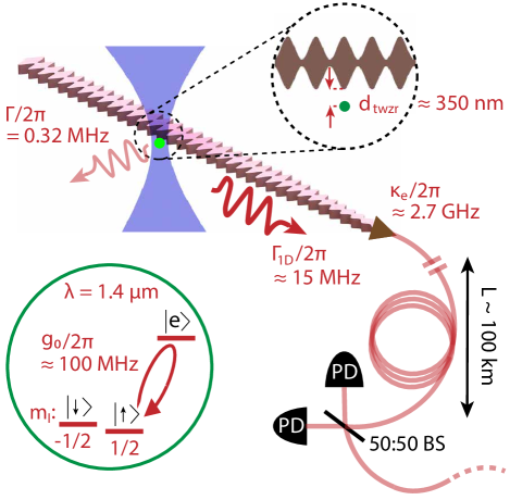
We focus on quantum communication as a specific application of this platform, and we envision an Yb atom coupled to a silicon nanophotonic cavity as a node in a quantum repeater network (Fig. 1). To this end, we propose a partially-open cavity design which enables the emission of MHz-bandwidth photons entangled with the nuclear spin of 171Yb that serves as a long-lived quantum memory. Further, we consider a fiber gap Fabry-Pérot cavity in Appendix III rather than a photonic crystal, which may offer a simpler alternative, but is not compatible with on-chip silicon photonics.
We highlight the use of silicon for the photonic crystal cavity not only due to low losses but also its maturity as a fabrication technology Almeida2004 . Robust and high-yield electronic, mechanical, and optical devices have been realized in silicon-based systems utilizing a wide array of highly developed micro- and nano-fabrication techniques. Indeed, custom silicon devices are increasingly commericially available from fabrication foundries (see e.g. Ref. Imec ). Moreover, silicon is compatible with other photonic technologies Miller2017 such as electro-optic Dieterle2016 ; Pitanti2015 and opto-mechanical Paraiso2015 ; Navarro2018 systems.
The precise control of single atoms in this approach enables scalable extension to multiple atoms by employing recently-demonstrated techniques with tweezer arrays Barredo2016 ; Endres2016 ; Kim2018a . This would enable photonic coupling within an array of atoms, which could lead to a novel platform for many-body physics Douglas2015 ; Hood2016 , quantum nonlinear optics Chang2014 ; Goban2015 , and photon-mediated quantum gates Welte2018 . The latter application is relevant to quantum repeaters, where deterministic two-qubit gates in each node could enhance entanglement distribution rates by realizing efficient Bell state measurements for entanglement swapping operations. Note that two-qubit gates could also be accomplished using local exchange Daley2008 ; Daley2011 ; Kaufman2015 or Rydberg Saffman2010 interactions.
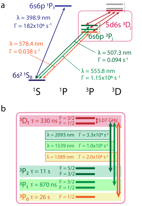
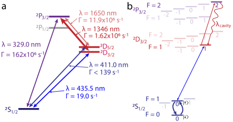
The strong telecom-wavelength transition of Yb is from a metastable state with lifetime sec (Fig. 2), which is the crutial state in the optical clock transition Ludlow2015 . We focus on the 1.4 m (3PD1) transition which is shown with the orange double arrow (see Appendix I). Concerning the other transitions available, the one at 1.5 m (3PD1) is hampered by the short lifetime of 3P1, which restricts its use to more complex protocols. Finally, the 2.1 m transition (3PD1) is not suitable for fiber-optic communication. However, it is an interesting candidate for free-space communication given the relatively high atmospheric transmission at this wavelength. We define the states of interest as , , and (see Figs. 1 & 3).
III Application in a quantum repeater
Before providing a detailed description of the photonic cavity and the coupling of the atom, we briefly highlight the potential of this platform for quantum communication (see Appendix II for more details). As an example, we consider utilizing our system in a quantum repeater architecture using the Barret-Kok scheme Barrett2005 ; Bernien2013 . The key parameters of our system that impact the entanglement generation rate and fidelity are summarized in Table 1. We describe in detail in the following sections how these values are achieved in our platform.
| Parameter | Section | Value |
|---|---|---|
| Bandwidth | IV | 2 MHz |
| Wavelength | II | 1.39 m (0.35 dB/km) |
| System efficiency | IV | 0.80 |
| Memory | II, AII | sec |
| Read-out fidelity | AII |
Our system allows a bandwidth of MHz, which is sufficiently high to not limit performance of the repeater. High bandwidth emission increases the detection fidelity since the acquisition time is reduced and detection of dark counts can be mitigated. While most emitter platforms have sufficient bandwidth, many of the platforms operating in the telecom band, such as rare-earth ions in crystals, have slow emission rates. The bare linewidth of erbium (Er) ions, for instance, is Hz Bottger2006 , and thus large Purcell enhancement in high-Q nanophotonic cavities Seidler2013 ; Asano2017 is required to enhance the emission rate.
The long-lived memory of the nuclear spin qubit is one of the strengths of our platform. Some atom-like defects such as nitrogen vacancy (NV) centers in diamond also have long memory Maurer2012 ; Reiserer2016 , but their optical transitions are at visible wavelengths and are hampered by phonon broadening. Further, many of the solid-state systems whose optical transitions are in the telecom band have short memories Probst2015 . In our system, the memory is assumed to be limited to the lifetime of the 3P0 state, though care must be taken to mitigate various heating mechanisms associated with tweezer trapping. A unique feature of alkaline-earth (-like) atoms is the possibility of cooling via electronic states while preserving coherence of the nuclear spin Daley2011 .
Another important characteristic for determining the quantum repeater performance is the system efficiency, which describes the probability that a photon emitted by the atom is acquired into the fiber network. This includes the coupling to the cavity, the extraction from the cavity into the waveguide, and the coupling to a fiber. All these values are described in Sec. IV, and the total photon system efficiency is expected to be .
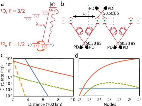
As a concrete demonstration of the potential of this system, we calculate the entanglement distribution rate in a network as shown in Fig. 3a and 3b, and compare it to direct communication without repeaters (see Appendix II for analysis). For a repeater system of 16 nodes we find that the distribution rate exceeds that of direct communication with a 10 GHz single photon source for a minimum total distance of 550 km. The corresponding entanglement distribution rate is 0.1 Hz. However, when local entanglement swapping at a node can be realized using two-qubit gates rather than probabilistic photon detection-based schemes, the distribution rate could be enhanced to 25 Hz. The distribution rate versus distance for 16 nodes is shown in Fig. 3c, and the rate versus number of nodes for 600 km is shown in Fig. 3d. These findings indicate that this platform is a competitive quantum repeater technology in the telecom band. Note that the fiber gap Fabry-Pérot alternative also performs well (see Appendix III).
IV The silicon photonic crystal cavity
We now describe the design of the partially-open cavity, and the resulting coupling strength to an Yb atom. We consider a photonic crystal geometry based on a nanobeam with an external corrugation Yu2014 . The sinusoidal modulation along the outer edges induces a photonic bandgap, which in turn enables the creation of a cavity via the introduction of a defect cell in the lattice to break the translational symmetry of the crystal. This enables the formation of modes localized in space around the defect region. For our chosen photonic crystal geometry, this is achieved by using a lattice constant nm. This is then subsequently tapered down to nm such that the relevant band-edge of the mirror region is tuned into the bandgap and hence establishes a cavity region.
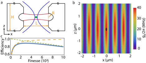
Details of the photonic crystal geometry are shown in Fig. 4a and b. The different colors show the different sections of the cavity. From left to right: purple is the input section of the cavity which transitions from a single mode waveguide to the photonic crystal geometry enabling the coupling of light in and out; medium blue is the left cavity mirror with higher transmission; dark green is the cavity taper region from the mirror cell lattice constant to the center cavity cell lattice constant ; light green is the central cavity unit cell; dark green is the taper to the backside mirror; and blue is the backside mirror with very high reflectivity. The tapering is done in such a way as to produce an effective quadratic potential for localized cavity photons, providing the optimal balance between localization in the plane of the device and radiation out-of-plane Srinivasan2002 ; Chan2009 ; Chan2012 . The device thickness is chosen to be 100 nm to extend the evanescent field due to weaker confinement inside the dielectric, hence allowing for a greater distance between the photonic crystal and the atom.
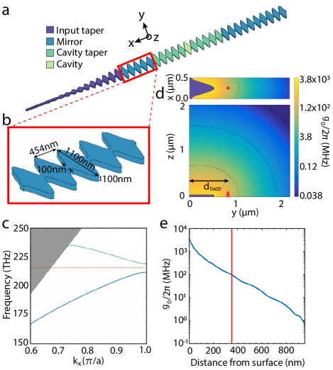
This design has a radiation limited quality factor of in simulations. However, we anticipate that the quality factor will be limited by intrinsic fabrication imperfections to , whose corresponding intrinsic cavity linewidth is MHz Fang2017 . We design the cavity to be partially open on one side (as in Fig. 4a) to efficiently extract the cavity photons Gallego2016 ; Gallego2018 ; Welte2018 . Specifically, we consider mirror cells on the front mirror and on the back mirror. The collection efficiency of extracting the photon into the waveguide mode is given by , where the subscript ‘’ denotes external coupling. In our design we have chosen a modest , for which and GHz.
We now consider the photonic mode profile. The transverse electric (TE) photonic band structure containing a bandgap centered on the atomic transition at nm (215.9 THz) is shown in Fig. 4c, and the evanescent field profile of the dielectric mode is shown in Fig. 4d. The blue ellipse and circle show the size of the atomic motional wavefunction, to be discussed in the next section. A line cut of the coherent coupling rate is shown in Fig. 4e for versus the distance from the surface, and we find an exponential length scale of nm. This is consistent with estimates for the mode dispersion based on the band structure (Fig. 4c). The position of the atom is represented by the vertical red line.
At the location of the maximal evanescent field, the electric field per photon is V/m. The vacuum Rabi frequency (i.e. coherent coupling rate) can then be calculated to be GHz at this location, and MHz at the chosen location of the atom nm, as explained in Sec. V. The single-atom cooperativity defined here as between a Yb atom and the silicon photonic crystal cavity can be estimated using the cavity linewidth and the atomic linewidth MHz. This corresponds to a cooperativity of . The Purcell-enhanced emission rate is given by the Purcell factor and the atomic decay rate as , which for this system gives MHz.
The probability of spontaneously emitting a photon into the cavity mode is given by , which is 0.98. Thus, the total efficiency of extracting the photon from the atom into the waveguide mode is given by , which is . We design the photonic cavity to taper to a nanobeam waveguide which can then be coupled to an optical fiber using a microlens or adiabatic coupler. Efficiencies for the latter are Tiecke2015 . These parameters result in a total system efficiency of .
V Trapping a single Yb atom near a photonic crystal
We now show that an Yb atom can be trapped close to the photonic crystal using only a tightly-focused optical tweezer.
V.1 Analysis of the optical tweezer trap
Single-atom detection and addressing of alkaline earth (-like) atoms is a growing area of research interest. Quantum gas microscopy of Yb has been demonstrated Yamamoto2016 , and large two-dimensional tweezer arrays of Yb Saskin2018 and strontium (Sr) Cooper2018 ; Norcia2018 have recently been reported. Further, cooling of single alkaline-earth (-like) atoms close to the motional ground state of an optical tweezer has recently been demonstrated for Sr Cooper2018 ; Norcia2018 , and cooling of alkali atoms optically trapped nm from a room-temperature surface has recently been observed Meng2018 .
For a tweezer wavelength of 473 nm (depending on the tweezer polarization Cooper2018 ), there is a ‘magic’ wavelength for which the polarizability of 1S0 and 3P1 are identical Beloy2012 ; Tang2017 . This is particularly useful for cooling the atom in the tweezer Cooper2018 ; Norcia2018 . Coincidentally, the polarizability of 3P0 is also similar Scazza2015t . Moreover, the polarizability at this wavelength is large, which allows deep traps to further mitigate surface forces. As such, we propose to use the nm wavelength for generating tightly-focused optical tweezers, although easily accessable wavelengths such as 532 nm are an alternate as they have been used in a similar magic configuration Yamamoto2016 ; Saskin2018 .
In order to further understand the design constraints and tweezer trap properties, we describe here the polarizability at the trapping wavelength , and the tweezer waist that can be generated with numerical aperture NA objective Yamamoto2016 . The polarizability of 1S0 and 3P1 at is Hz/(W/cm2) Scazza2015t . For an objective of NA, the waist radius of a tweezer that can be generated with this wavelength is nm, and the corresponding Rayleigh range is nm. An optical power of 1.0 mW is required for a trap depth of mK, and the trapping frequencies are kHz and kHz. The polarizability of the 3D1 state is not well known, but it is only populated during a -pulse for photon-spin entanglement and during read-out (see Appendix II). To mitigate deleterious effects from a polarizability mismatch on the 3PD1 transition, we propose to switch the trap off during excitation Tiecke2014 . Atom survival probability in the absence of a trap is known to be high for times of several s Bernien2017 , which is much longer than the Purcell enhanced emission timescale ns.
The temperature of a typical Yb magneto-optical trap (MOT) operating on the 1S0 - 3P1 transition is K Scazza2015t ; Yamamoto2016 . This temperature would correspond to motional quanta in the radial direction and motional quanta in the axial direction, and further cooling in a tweezer has been demonstrated with Sr Cooper2018 ; Norcia2018 . Such conditions lead to thermal atomic wavefunction radii of nm in the radial direction and nm in the axial direction. The circles in Figs. 4d are meant to roughly represent the size of the atomic wavefunction and illustrate how small it is compared to the mode profile of the cavity field. Note that the nodal spacing of the cavity is larger here compared to previous work Thompson2013a because of the longer wavelength, and thus the evanescent field coupling is expected to be more homogeneous over the tweezer trap volume.
V.2 Atom trapping and imaging near the photonic crystal
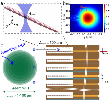
We consider a tweezer focused at a distance d nm from the photonic crystal, as shown in Fig. 5a and 5b. This was chosen to be slightly larger than the waist of the tweezer nm to minimize the impact of scattered fields from the photonic crystal. Further, we propose to use the chip geometry shown in Fig. 5c and discussed in the next subsection, which allows the tweezer to be translated with respect to the cavities on the chip and the MOT Thompson2013a using an acousto-optic deflector or spatial light modulator. This is advantageous since atomic flux on the device is known to have detrimental effects on photonic structures Ritter2015 ; Ritter2016 .
A significant difference between alkali- and alkaline-earth(-like) atoms is the size and temperature of their MOTs. For alkalis, typically only one atomic transition is used for laser cooling and optical molasses. Conversely, alkaline-earth(-like) atoms are typically laser cooled in two stages: the broad 1SP1 transition for initial loading and the narrow 1SP1 transition for cooling to K Scazza2015t ; Yamamoto2016 as mentioned above. Further, the narrow linewidth of the cooling transition in the second stage allows for flexibility in the MOT size and position by adjusting the magnetic field gradient and offset. Hence, a small and cold second-stage ‘green’ MOT could be moved to m off the silicon chip using magnetic fields, which is within the field of view of typical microscope objectives. This enables easy tweezer transport with acousto-optic deflectors Endres2016 (see Fig. 5), and does not require translation of the objective. The large first-stage ‘blue’ MOT could be millimeters from the chip at all times. This approach will reduce atomic flux onto the device compared to previous work Thompson2013a ; Goban2013 , and also mitigates the detrimental effect of the photonic structure on the MOT.
Surface effects on the atom are substantially mitigated in our approach compared to previous work Thompson2013a . Operating at 350 nm from the surface instead of 200 nm decreases the surface potential to %, and surface force to % to that of previous work Thompson2013a (see Supplementary Material in Ref. Thompson2013a , and Ref. Derevianko2010 for electric dipole polarizabilities at imaginary frequencies used in this calculation). In addition, the external corregation used in our photonic crystal design further reduces the effective surface area interacting with the atom where only the surface areas at the antinodes (see Fig. 1 and 5b) contribute significantly to the surface force. We can compare this surface force with the dipole force in the tweezer potential. We expect the surface force to be 100’s of kHz/m or less, while the maximum dipole force for a tweezer as described above with 1 mK depth is MHz/m, and the use of deeper traps is possible.
Now we consider absorption of the tweezer light by the silicon nanocavity. Absorption can have two deleterious effects: it can cause heating of the structure that will alter the cavity properties, and it can generate free-carriers which increase the optical absorption in the telecom band Barclay2005 ; Johnson2006 . The absorption coefficient of silicon at a wavelength of nm is cm-1 Bucher1994 , which means that of incident tweezer light will be absorbed by our cavity of 100 nm thickness. For a 1 mW tweezer of waist nm at a distance from the surface of nm, we estimate that W is incident on the device, and thus nW is absorbed. Given the thermal conductivity of silicon and the dimensions of the proposed nanocavity we expect a K temperature difference in the vicinity of the tweezer relative to the chip which serves as a thermal reservoir. The temperature dependence of the index of refraction causes a shift in the cavity resonance frequency at the /K level Barclay2005 . Hence, we expect fractional shift in the cavity resonance, which is much less than for the cavity.
To mitigate the effect of free-carrier generation in the silicon nanocavity, we propose to switch the tweezer off during the telecom-photon emission phases, such as spin-photon entanglement and read-out. The weak tweezer illumination onto the device will cause free electron-hole pairs which will decay within 10’s of ns Barclay2005 ; Johnson2006 . This is fast compared to the allowed free expansion time of the atom with high probability re-trapping (several s), so waiting for 100’s of ns to ensure electron-hole pair decay is feasible. Since the recoil energy of a telecom photon is low, we expect heating of the atom during these pulses to be sufficiently small.
Coherent scattering from the nanocavity must also be considered because it could alter the trapping potential. We calculate the trapping potential in the presence of scattering from the silicon device using a finite-difference time-domain simulation. We simulate a gaussian beam with a waist of 330 nm focused at a distance of nm from the edge of the photonic crystal cavity. The results are shown in Fig. 5b, where the magnitude of the electric field is shown on a relative scale. The trap perturbations are below (), and they occur only at distances of from the center of the tweezer. This effect is negligible, particularly for a cold atom.
The ability to have many photonic cavities per chip facilitates fabrication error and device degradation to be overcome, but also opens the possibility to couple an array of atoms in optical tweezers Endres2016 to an array of cavities. This would enable multi-qubit repeater nodes as discussed in Sec. II, III, and Appendix II. An array of cavities can be fabricated such that their separation is as small as m (as in Fig. 5c). The cavities are coupled to a microlens coupler or adiabatic coupler, and the fiber could be aligned and coupled to any individual cavity on the chip using a three-axis stage as shown in Fig. 5c. Each cavity is independently temperature controlled with its own tungsten heating strip (light blue lines in Fig. 5c), and thus each cavity in the array could be individually tuned into resonance with the atomic transition Kim2016 . This strip is also used for applying radio-frequency (RF) pulses to control the nuclear spin (Appendix II).
VI Conclusion and outlook
We have illustrated that silicon-based photonics combined with tweezer-trapped 171Yb atoms are a candidate system for quantum optics in the telecom-band. The strong m transition from the 3P0 ‘clock’ state of Yb enables 15 MHz-bandwidth emission when coupled to a silicon photonic cavity, and the nuclear spin allows for a coherent quantum memory. Further, we propose a simple and robust trapping protocol which enables atoms to be coupled to silicon nanophotonics, and even facilitates an array of atoms coupled to an array of cavities. Furthermore, we illustrate the potential of our platform for quantum repeaters.
Moreover, there are several other applications of this system which include quantum photonic circuits, novel platforms for long-range interactions, and many-body physics Douglas2015 . Our system may enable the direct integration of neutral-atom quantum computers into a quantum network, in which quantum gates can be performed using local exchange Daley2011 ; Kaufman2015 or Rydberg Saffman2010 interactions. Further, this system opens the possibility to implement an optical clock network Komar2014 by using the 1SP0 optical clock qubit Ludlow2015 .
Alternative cavity designs based on free-space optics could offer different possibilities, and we consider a fiber Fabry-Pérot cavity in Appendix III. Finally we note that a similar telecom-wavelength atomic system could be created with Yb+ ions, where a group of transitions from a metastable state has convenient wavelengths of 1450 and 1650 nm. We analyze a Yb+ ion coupled with a fiber Fabry-Pérot cavity in Appendix IV, but we note that ion trapping near dielectric materials poses other technical challenges.
Acknowledgements
We acknowledge Mohammad Mirhosseini, Alexandre Cooper-Roy, and Matthew D. Shaw for useful discussions, and Hengjiang (Jared) Ren with help with COMSOL simulations. We also ackowledge Hannes Bernien and Jeff Thompson for critical reading of the manuscript. JPC acknowledges support from the Caltech PMA Division for post-doctoral fellowship funding, AS acknowledges support from the Caltech IQIM for post-doctoral fellowship funding, and NS acknowledges funding by the Alliance for Quantum Technologies’ Intelligent Quantum Networks and Technologies (INQNET) research program. We acknowledge funding provided by the Institute for Quantum Information and Matter, an NSF Physics Frontiers Center (NSF Grant PHY-1733907). This work was also supported by the NSF CAREER award, the Sloan Foundation, and by the NASA/JPL President’s and Director’s Fund.
APPENDIX I Dipole matrix elements and polarization considerations
In order to quantify the coupling to a cavity we must calculate the dipole matrix element of the desired atomic transition: (see Appendix II for detailed quantum repeater scheme). The 3PD1 transition has been carefully measured because of its relevance to Yb clock precision Beloy2012 . Given that s-1, we arrive at C-m, or 1.63 a0-e, in which the polarization is taken to be (). However, purely circular polarization cannot be supported by the modes of the photonic structure (see Sec. IV), and so the effective dipole matrix element is reduced by upon decomposing into a combination of linear polarizations. The ‘quantization axis’ is assumed to be determined by the electric field of the optical tweezer (see Sec. IV), and the external magnetic field (see Appendix II) is assumed to be parallel. To drive the transition, we require the electric field of the mode in the cavity to be perpendicular to the quantization field axis .
APPENDIX II Quantum repeater implementation
In this section we describe a quantum repeater based on a network of 171Yb atoms coupled to photonic crystal cavities. The repeater involves dividing a long channel of length into elementary links of length that are connected by nodes which feature a pair of trapped atoms. The integer is often referred to as the number of nesting levels Sangouard2011 . Atom-atom entanglement that spans is achieved by entangling atoms that are separated by and by performing entanglement swapping between atoms that are located at each node. Fig. 3b depicts two elementary links and entanglement swapping at one node. We consider the scheme of Barrett and Kok Barrett2005 ; Bernien2013 for generation of remote spin-spin entanglement and then calculate the rate of distribution of a Bell state.
APPENDIX II.1 Level scheme and protocol
We consider the three-levels of 171Yb shown in Fig. 3a using solid colors. These consist of an excited Zeeman level of the 3D1 manifold and a pair of nuclear spin levels of the 3P0 manifold that form the ground level. The 3P0 state can be populated from the 1S0 ground state by using the ‘clock’ transition Ludlow2015 , or by multi-photon processes Barker2016 . The and Zeeman levels of the 3D1 level are separated by 0.47 MHz/G, which is much larger than the 752 Hz/G splitting of the levels of 3P0.
The first step of the repeater is to generate spin-photon entanglement and then, using two-photon detection, spin-spin entanglement between atoms that are separated by one elementary link. We begin by preparing each atom in an equal superposition of the nuclear states of the 3P0 ground level: . This is accomplished by a RF field despite the relatively small gyromagnetic ratio of the spin Hz/G. Nonetheless, this favorably results in a weak coupling of the spin to the environment Boyd2007 ; Gorshkov2009 . We propose to split these states with a magnetic field of G. With the fabricated micro-stripline resonator Robledo2011a described in Sec. V, we expect Rabi frequencies of tens of kilohertz using tens of Watts of RF power. This allows -pulses to be performed on timescales that are much less than the time to establish entanglement over an elementary link (see Subsec. B).
Next, each atom is excited by a short laser pulse that is resonant with the transition, as indicated by in Fig. 3a. As described in Sec. V, this transition is strongly-coupled to the cavity, and thus the resultant spontaneous emission locally entangles the spin and photon number in the Bell state , in which 1(0) represents the presence (absence) of an emitted photon.
The photons that are emitted by each atom are directed to a beam splitter which is located half-way between nodes, see Fig. 3b. If the photons that are emitted by each atom are indistinguishable, detection of one photon after the beam splitter heralds spin-spin entanglement or, due to potential loss and imperfections, a spin-spin product state between each atom Barrett2005 ; Bernien2013 . To avoid the latter, a -pulse inverts the spins and the transition is optically excited a second time. The detection of a photon in both rounds heralds the creation of a spin-spin Bell state between each atom , in which the relative phase is defined according to whether both photons were detected on the same or different output ports of the beam splitter.
Entanglement swapping is accomplished by performing a similar procedure as to generate heralded entanglement– optical excitation, single photon detection, spin flip, and detection of a second photon. This procedure limits the swapping efficiency to at most 50% Calsamiglia2001 . A deterministic swapping process, which allows improved scaling, could be achieved by trapping two atoms using two tweezers within a single cavity and exploiting photon-mediated deterministic intracavity gates Douglas2015 .
A limitation of this process will be the isolation of the transition relative to the other transitions in the 3D1 state (see Fig. 3a). The splitting between the and states is 470 kHz/G, and this must be compared to the Purcell-enhanced linewidth . We choose a field of G for which MHz. For MHz and Rabi frequency , the off-resonant scattering rate is kHz. The read-out fidelity is assumed to be , which is . Note that this value is even slightly improved when considering the Clebsch-Gordan coefficients for the different pathways.
APPENDIX II.2 Entanglement distribution rate
We quantify the distribution rate of a Bell state using our repeater scheme, showing that it outperforms an approach based on the direct transmission of photons. We denote the success probability for an atom to emit a photon into a single mode fiber (e.g. system efficiency) to be , which includes the probability to prepare the initial state, the spontaneous emission of a photon into the cavity mode, and the coupling into a fiber. The probability of the two-photon measurement at the center of the elementary link is given by in which is the fiber transmission with attenuation length km. This corresponds to losses of 0.35 dB/km at 1.4 m using hydrogen-aged single mode fiber, which has been recently deployed for modern infrastructure (see, e.g., Corning SMF-28e for ITU-T G.562D standards Napoli2017 ).
The spin-spin entanglement creation step is repeated at time intervals of the communication time , in which m/s is the speed of light in fiber. Thus, the average time to produce entanglement that spans an elementary link is . Using the beam splitter approach depicted in Fig. 3b, the efficiency of the entanglement swapping operation is , while a deterministic gate allows , assuming the gate fidelity is unity. Therefore, the total time for the distribution of an entangled pair over distance 2 is given by , and the average time to distribute an entangled pair over distance is . The factor of 3/2 arises because entanglement has to be created over two links before the swapping is performed Sangouard2009 ; Sangouard2011 .
For the discussion in Section III we assume , which is given by the estimated in Sec. IV, a detection efficiency of 0.9, and that the lifetime of the 3P0 level is much longer than the distribution time. This detection efficiency is straightforwardly achieved using superconducting nanowires, which have been demonstrated at 1.5 m Marsili2013 . Note that the spontaneous Purcell-enhanced emission time from 3D1 is ns, which is negligible compared to the time to distribute entanglement over an elementary link. Figs. 3c and 3d show the repeater performance based on this analysis, plotted versus total distance for nodes (3c) and versus number of nodes for a total distance of 600 km (3d).
APPENDIX III Coupling Yb to a fiber gap Fabry-Pérot cavity
In this section, we discuss an alternative approach to efficiently interface a single atom with a single telecom photon in a fiber using fiber based Fabry-Pérot (FP) resonator Steinmetz2006 ; Colombe2007 ; Hunger2010 . While fiber based Fabry-Pérot resonators have significantly larger mode volumes () that result in reduced vacuum Rabi frequencies, we show that they can achieve high enough cooperativities necessary to extract single photons directly into a telecom fiber with sufficiently high efficiency.
We begin by considering the geometry of fiber FP cavities, as shown in Fig. 6a. Typical heights of the cavity claddings are 125 m, so in order to focus a tweezer and image an atom inside with high NA, we assume a cavity length m. We choose radii of curvature of the cavity mirrors to be m, which is a typical value for such CO2-laser etching techniques Hunger2010 . This geometry at a wavelength of nm gives a mode waist of m and a mode volume of m3, or .
We also analyze the mode profile in this cavity in a similar way to the photonic cavity, and a zoom-in of the central m is shown in Fig. 6b. The black ellipse shows a liberal estimate of the atomic wavefunction in a tweezer as described in the previous section. The only requirement in this system is that the atom is centered on the antinode as shown in Fig. 6b. Noting that the -axis into the page has the same profile as the -direction, this system requires an overall less precise alignment than the photonic cavity.
The coherent coupling rate between the cavity and the atom is given by Hunger2010
| (1) |
where is the reduced dipole matrix element, is the angular frequency of the cavity and the atomic transition, is the permittivity of free space. For this geometry and the value of discussed above, we obtain a coherent coupling rate of MHz. Note that here the cavity supports two degenerate polarizations, so the cavity field can have perfect polarization overlap with the transition dipole. As with the photonic crystal cavity, we design the fiber cavity such that one mirror has lower reflection and allows for coupling photons into and out of the cavity Gallego2016 ; Gallego2018 ; Welte2018 . Now we choose a finesse of , which is well below maximum finesse values of Hunger2010 . The cavity linewidth for these values is MHz, and the free spectral range THz.
We can now estimate the single-atom cooporativity Hunger2010 , defined here for consistency with the photonic crystal as . For our values we arrive at , for which the probability of emission of a spontaneous photon into the cavity mode is . We assume an intrinsic finesse of Hunger2010 ; Gallego2016 , for which we can again define a collection efficiency of extracting the photon into the waveguide mode, which is given by . For this corresponds to . The efficiency of extracting a photon from the atom into the waveguide mode is given by the product of these , which is 0.94. is maximized for , as is shown in Fig. 6c.
However, another factor emerges because we require the waveguide mode of the optical fiber to be single-mode (SM). This is necessary since indistinguishable photons are required for Bell state measurements. Representative efficiencies for coupling a photon in a cavity similar to our design into a SM fiber are Hunger2010 . The photon acquisition efficiency is thus .
As with the photonic crystal in the main text, we show a table for the fiber FP cavity of the quantities relevant for a quantum repeater in Table 2. The Purcell-enhanced linewidth is given by , where . For the fiber FP cavity MHz. For the same G and for , we get kHz, and .
| Parameter | Section | Value |
|---|---|---|
| Bandwidth | AIII | 2 MHz |
| Wavelength | II | 1.39 m (0.35 dB/km) |
| System efficiency | AIII | 0.80 |
| Memory | II, AII | sec |
| Read-out fidelity | AIII |
APPENDIX IV Telecom networks with Yb+ ions
We now discuss the possibility of using Yb+ ions in fiber FP cavities. Yb+ has strong telecom transitions that remain largely unused in experiments. Yet, they have been studied carefully by theorists because Yb is a platform for parity violation measurements Safronova2009 ; Dzuba2011 ; Sahoo2011 ; Porsev2012 ; Feldker2017 . Similar to the scheme in neutral Yb, the telecom transitions in Yb+ are from metastable states 2D3/2 and 2D5/2, which are strongly coupled to a higher-lying state 2P3/2 via wavelengths of 1346 nm and 1650 nm, respectively. The relevent level structure is shown in Fig. 7a. The metastable 2D3/2 and 2D5/2 states are very weakly connected to the ground state via ‘clock’-like transitions, similar to the case of neutral Yb.
The scheme described in Fig. 7b is designed to include the ground-state hyperfine qubit, which has become the workhorse of quantum information processing with trapped ions. One of these qubit states can be mapped to the 2D3/2 manifold by driving the electric quadrupole (E2) ‘clock’ transition Schneider2005 . An excitation from this state to the P3/2 allows one of the ground hyperfine qubit states to be entangled with a telecom photon that is strongly coupled to the cavity. The mapping back to the ground state is done by performing a -pulse with the ‘clock’ laser.
We choose the 2D3/2 state rather than 2D5/2 because it is easier to eliminate other decay pathways from the 2P3/2 excited state. The hyperfine splitting is 430 MHz for 2D3/2 but only 64 MHz for 2D5/2 Feldker2017 . This latter value is comparable to the Purcell-enhanced linewidth for the decay into the cavity mode. Note that the dipole matrix is 4.2 a0-e for the transition from 2P3/2 to 2D5/2 and 1.3 a0-e for the transition to 2D3/2 Porsev2012 . The Purcell-enhanced linewidth for the 2D3/2 state in a fiber FP cavity is well below the hyperfine splitting of 430 MHz.
Using Equations 2 and 3 above, we can arrive at the exact DME for the specific scheme described in Fig. 7b. This gives DME a0-e. This is smaller than the case for neutral Yb by a factor of even though the linewidth is similar. This is because , and thus there is hyperfine splitting and more states that contribute to the total linewidth.
We believe that the fiber FP cavity considered above and in Fig. 6 is also suitable for Yb+. Indeed, a Yb+ ion has already been trapped inside a fiber cavity, where the fiber length is m Steiner2013 . In that work, the same metastable state 2D3/2 was used, but it was coupled to an even higher excited state 3D (not shown), with a transition wavelength of 935 nm. The atomic wavefunction in an ion trap is of similar size to that in an optical tweezer, so the entire discussion above and in Fig. 3 applies here as well.
As for the neutral Yb scheme described above, this scheme for Yb+ ion could be used for creating a clock network. This transition is already used for atomic ion frequency standards Schneider2005 , and so the development of a commercial technology based on this system may be more straightforward. Further, such a scheme could allow direct telecommunications between trapped ion quantum computers to facilitate the realization of a quantum computing network Duan2010 , and it could also be used with multiple qubits at each node of the network, for which gate operations between qubits can be employed for error correction or decoherence free subspaces Zwerger2017 .
References
- (1) L.-M. Duan and C. Monroe, Rev. Mod. Phys. 82, 1209 (2010).
- (2) A. Reiserer and G. Rempe, Rev. Mod. Phys. 87, 1379 (2015).
- (3) J. I. Cirac, P. Zoller, H. J. Kimble, and H. Mabuchi, Phys. Rev. Lett. 78, 3221 (1997).
- (4) S. J. van Enk, J. I. Cirac, and P. Zoller, Science 279, 205 (1998).
- (5) H. J. Kimble, Nature 453, 1023 (2008).
- (6) S. Wehner, D. Elkouss, and R. Hanson, Science 362 (2018).
- (7) M. Uphoff, M. Brekenfeld, G. Rempe, and S. Ritter, Applied Physics B 122, 46 (2016).
- (8) O. Alibart et al., Journal of Optics 18, 104001 (2016).
- (9) D. E. Chang, J. S. Douglas, A. González-Tudela, C.-L. Hung, and H. J. Kimble, Rev. Mod. Phys. 90, 031002 (2018).
- (10) M. Bock et al., arXiv:1710.04866v1 (2017).
- (11) A. Sipahigil et al., Science 354, 847 (2016).
- (12) A. M. Dibos, M. Raha, C. M. Phenicie, and J. D. Thompson, Phys. Rev. Lett. 120, 243601 (2018).
- (13) F. K. Asadi et al., arXiv:1712.05356v1 (2017).
- (14) K. Kutluer, M. Mazzera, and H. de Riedmatten, Phys. Rev. Lett. 118, 210502 (2017).
- (15) T. Zhong et al., Science 357, 1392 (2017).
- (16) A. Goban et al., Nature Communications 5, 3808 (2013).
- (17) J. D. Thompson et al., Science 340, 1202 (2013).
- (18) T. G. Tiecke et al., Nature 508, 241 (2014).
- (19) D. E. Chang, V. Vuletic, and M. D. Lukin, Nature Photonics 8, 685 (2014).
- (20) A. Goban et al., Phys. Rev. Lett. 115, 063601 (2015).
- (21) I. Aharonovich, D. Englund, and M. Toth, Nature Photonics 10, 631 (2016).
- (22) D. D. Awschalom, R. Hanson, J. Wrachtrup, and B. B. Zhou, Nature Photonics 12, 516 (2018).
- (23) E. Vetsch et al., Phys. Rev. Lett. 104, 203603 (2010).
- (24) A. Goban et al., Phys. Rev. Lett. 109, 033603 (2012).
- (25) M. E. Kim, T.-H. Chang, B. M. Fields, C.-A. Chen, and C.-L. Hung, arXiv:1810.08769v1 (2018).
- (26) J. M. McGuirk, D. M. Harber, J. M. Obrecht, and E. A. Cornell, Phys. Rev. A 69, 062905 (2004).
- (27) D. Hunger et al., Phys. Rev. Lett. 104, 143002 (2010).
- (28) J. M. Obrecht, R. J. Wild, and E. A. Cornell, Phys. Rev. A 75, 062903 (2007).
- (29) M. Antezza, L. P. Pitaevskii, and S. Stringari, Phys. Rev. A 70, 053619 (2004).
- (30) Y.-j. Lin, I. Teper, C. Chin, and V. Vuletić, Phys. Rev. Lett. 92, 050404 (2004).
- (31) J. M. Obrecht et al., Phys. Rev. Lett. 98, 063201 (2007).
- (32) N. Schlosser, G. Reymond, I. Protsenko, and P. Grangier, Nature 551, 485 (2017).
- (33) A. M. Kaufman, B. J. Lester, and C. A. Regal, Phys. Rev. X 2, 041014 (2012).
- (34) J. D. Thompson, T. G. Tiecke, A. S. Zibrov, V. Vuletić, and M. D. Lukin, Phys. Rev. Lett. 110, 133001 (2013).
- (35) V. R. Almeida, C. A. Barrios, R. R. Panepucci, and M. Lipson, Nature 431, 1081 (2004).
- (36) https://www.imec-int.com/en/integrated-silicon-photonics, Leuven, Belgium (https://www.imec-int.com/en/home).
- (37) S. A. Miller et al., Optica 4, 707 (2017).
- (38) P. B. Dieterle, M. Kalaee, J. M. Fink, and O. Painter, Phys. Rev. Applied 6, 014013 (2016).
- (39) A. Pitanti et al., Opt. Express 23, 3196 (2015).
- (40) T. K. Paraïso et al., Phys. Rev. X 5, 041024 (2015).
- (41) D. Navarro-Urrios et al., Opt. Express 26, 9829 (2018).
- (42) D. Barredo, S. de Léséleuc, V. Lienhard, T. Lahaye, and A. Browaeys, Science (2016).
- (43) M. Endres et al., Science 354, 1024 (2016).
- (44) J. S. Douglas et al., Nature Photonics 9, 326 (2015).
- (45) J. D. Hood et al., Proceedings of the National Academy of Sciences 113, 10507 (2016).
- (46) S. Welte, B. Hacker, S. Daiss, S. Ritter, and G. Rempe, Phys. Rev. X 8, 011018 (2018).
- (47) A. J. Daley, M. M. Boyd, J. Ye, and P. Zoller, Phys. Rev. Lett. 101, 170504 (2008).
- (48) A. J. Daley, Springer Quantum Inf Process (2011).
- (49) A. M. Kaufman et al., Nature 527, 208 (2015).
- (50) M. Saffman, T. G. Walker, and K. Mølmer, Rev. Mod. Phys. 82, 2313 (2010).
- (51) A. D. Ludlow, M. M. Boyd, J. Ye, E. Peik, and P. O. Schmidt, Rev. Mod. Phys. 87, 637 (2015).
- (52) S. D. Barrett and P. Kok, Phys. Rev. A 71, 060310 (2005).
- (53) H. Bernien et al., Nature 497, 86 (2013).
- (54) T. Böttger, Y. Sun, C. W. Thiel, and R. L. Cone, Phys. Rev. B 74, 075107 (2006).
- (55) P. Seidler, K. Lister, U. Drechsler, J. Hofrichter, and T. Stöferle, Opt. Express 21, 32468 (2013).
- (56) T. Asano, Y. Ochi, Y. Takahashi, K. Kishimoto, and S. Noda, Opt. Express 25, 1769 (2017).
- (57) P. C. Maurer et al., Science 336, 1283 (2012).
- (58) A. Reiserer et al., Phys. Rev. X 6, 021040 (2016).
- (59) S. Probst, H. Rotzinger, A. V. Ustinov, and P. A. Bushev, Phys. Rev. B 92, 014421 (2015).
- (60) S. Pirandola, R. Laurenza, C. Ottaviani, and L. Banchi, Nature communications 8, 15043 (2017).
- (61) S.-P. Yu et al., Applied Physics Letters 104, 111103 (2014).
- (62) K. Srinivasan and O. Painter, Opt. Express 10, 670 (2002).
- (63) J. Chan, M. Eichenfield, R. Camacho, and O. Painter, Opt. Express 17, 3802 (2009).
- (64) J. Chan, A. H. Safavi-Naeini, J. T. Hill, S. Meenehan, and O. Painter, Applied Physics Letters 101, 081115 (2012).
- (65) K. Fang et al., Nature Physics 13, 465 (2017).
- (66) J. Gallego et al., Applied Physics B 122, 47 (2016).
- (67) J. Gallego et al., arXiv:1804.08526v1 (2018).
- (68) T. G. Tiecke et al., Optica 2, 70 (2015).
- (69) R. Yamamoto, J. Kobayashi, T. Kuno, K. Kato, and Y. Takahashi, New Journal of Physics 18, 023016 (2016).
- (70) S. Saskin, J. T. Wilson, B. Grinkemeyer, and J. D. Thompson, arXiv:1810.10517v1 (2018).
- (71) A. Cooper et al., arXiv:1810.06537 (2018).
- (72) M. A. Norcia, A. W. Young, and A. M. Kaufman, arXiv:1810.06626v1 (2018).
- (73) Y. Meng, A. Dareau, P. Schneeweiss, and A. Rauschenbeutel, Phys. Rev. X 8, 031054 (2018).
- (74) K. Beloy et al., Phys. Rev. A 86, 051404 (2012).
- (75) Z.-M. Tang, Y.-M. Yu, J.-G. Li, and C.-Z. Dong, Journal of Physics: Conference Series 875, 022050 (2017).
- (76) F. Scazza, PhD thesis, Ludwig-Maximilians-Universitat Munchen (2015).
- (77) H. Bernien et al., Nature 551, 579 (2017).
- (78) R. Ritter et al., Applied Physics Letters 107, 041101 (2015).
- (79) R. Ritter et al., New Journal of Physics 18, 103031 (2016).
- (80) A. Derevianko, S. G. Porsev, and J. F. Babb, Atomic Data and Nuclear Data Tables 96, 323 (2010).
- (81) P. E. Barclay, K. Srinivasan, and O. Painter, Opt. Express 13, 801 (2005).
- (82) T. J. Johnson, M. Borselli, and O. Painter, Opt. Express 14, 817 (2006).
- (83) K. Bücher, J. Bruns, and H. G. Wagemann, Journal of Applied Physics 75, 1127 (1994).
- (84) J.-H. Kim, C. J. K. Richardson, R. P. Leavitt, and E. Waks, Nano Letters 16, 7061 (2016).
- (85) P. Komar et al., Nature Physics 10, 582 (2014).
- (86) N. Sangouard, C. Simon, H. de Riedmatten, and N. Gisin, Rev. Mod. Phys. 83, 33 (2011).
- (87) D. S. Barker, N. C. Pisenti, B. J. Reschovsky, and G. K. Campbell, Phys. Rev. A 93, 053417 (2016).
- (88) M. M. Boyd et al., Phys. Rev. A 76, 022510 (2007).
- (89) A. V. Gorshkov et al., Phys. Rev. Lett. 102, 110503 (2009).
- (90) L. Robledo et al., Nature (London) 477, 574 (2011).
- (91) J. Calsamiglia and N. Lütkenhaus, Applied Physics B 72, 67 (2001).
- (92) A. Napoli and J. Pedro, Fibre Systems, Viewpoint (2017).
- (93) N. Sangouard, R. Dubessy, and C. Simon, Physical Review A 79, 042340 (2009).
- (94) F. Marsili et al., Nature Photonics 7, 210 (2013).
- (95) T. Steinmetz et al., Applied Physics Letters 89, 111110 (2006).
- (96) Y. Colombe et al., Nature 450, 272 (2007).
- (97) D. Hunger et al., New Journal of Physics 12, 065038 (2010).
- (98) U. I. Safronova and M. S. Safronova, Phys. Rev. A 79, 022512 (2009).
- (99) V. A. Dzuba and V. V. Flambaum, Phys. Rev. A 83, 052513 (2011).
- (100) B. K. Sahoo and B. P. Das, Phys. Rev. A 84, 010502 (2011).
- (101) S. G. Porsev, M. S. Safronova, and M. G. Kozlov, Phys. Rev. A 86, 022504 (2012).
- (102) T. Feldker, H. Furst, N. V. Ewald, J. Joger, and R. Gerritsma, arXiv:1711.10368v1 (2017).
- (103) T. Schneider, E. Peik, and C. Tamm, Phys. Rev. Lett. 94, 230801 (2005).
- (104) M. Steiner, H. M. Meyer, C. Deutsch, J. Reichel, and M. Köhl, Phys. Rev. Lett. 110, 043003 (2013).
- (105) M. Zwerger et al., Quantum Science and Technology 2, 044001 (2017).