Optical absorption properties of few-layer phosphorene
Abstract
We investigate the optical absorption and transmission of few-layer phosphorene in the framework of ab initio density functional simulations and many-body perturbation theory at the level of random phase approximation. In bilayer phosphorene, the optical transition of the valence band to the conduction band appears along the armchair direction at about 0.72 eV, while it is absent along the zigzag direction. This phenomenon is consistent with experimental observations. The angle-resolved optical absorption in few-layer phosphorene shows that it is transparent when illuminated by near grazing incidence of light. Also, there is a general trend of an increase in the absorption by increasing the number of layers. Our results show that the bilayer phosphorene exhibits greater absorbance compared to that of bilayer graphene in the ultraviolet region. Moreover, the maximal peak in the calculated absorption of bilayer MoS2 is in the visible region, while bilayer graphene and phosphorene are transparent. Besides, the collective electronic excitations of few-layer phosphorene are explored. An optical mode (in-phase mode) that follows a low-energy dependence for all structures, and another which is a damped acoustic mode (out-of-phase mode) with linear dispersion for multilayer phosphorene are obtained. The anisotropy of the band structure of few-layer phosphorene along the armchair and zigzag directions is manifested in the collective plasmon excitations.
pacs:
73.20.Mf, 71.10.Ca, 71.15.-m, 78.67.WjI Introduction
Advanced two-dimensional (2D) crystalline layered materials have received great attention during the past decade. The most well-known 2D crystalline materials are graphene zhang ; asgari and molybdenum disulfide wang_2012 . The gapless nature of graphene and a low carrier mobility of transition metal dichalcogenides (TMDCs) have limited their potential applications in technology and electronic devices wang_2015 . Phosphorene, one or a few layers of black phosphorous Liu , is another 2D semiconductor that has lately become the focus of investigations owing to its high carrier mobilities and a tunable band gap qiao ; peng . High charge mobility on the order of cm2/Vs has been observed in monolayer phosphorene at low temperatures warsch . Also, the narrow gap of phosphorene (between zero-gap graphene and large-gap TMDCs), makes it an ideal material for near and mid-infrared optoelectronics and new types of plasmonic devices xia2014 .
Similar to graphene and TMDCs, phosphorene is also a layered material that can be exfoliated to yield individual layers Lu . Monolayer phosphorene with a hexagonal puckered lattice has a direct band gap and high anisotropic band structure. The dispersion relation in monolayer phosphorene is highly anisotropic, which gives rise to the direction depending on mechanical, optical, electronic and transport properties wang_nano ; jin_2016 ; zare_2017 ; nourbakhsh . Bilayer phosphorene has attracted considerable interest given its potential application in nanoelectronics owing to its natural band gap and high carrier mobility zhang_bi ; Tran2014 ; Dai_bi . Bilayer phosphorene has a smaller direct band gap than monolayer phosphorene, which offers more opportunity to tune the semiconductor, metal and maybe even topological insulator Liu . More efforts have been devoted to the band structure and electronic properties of few-layer phosphorene, however, its optical properties deserve special consideration. Most importantly, phosphorene exhibits strong light-matter interactions in the visible and infrared photon energies. The application of few-layer phosphorene in nanoplasmonics and terahertz devices is highly promising Buscema ; Tran .
The aim of this paper is to explore the angle-resolved optical absorption and transmission of few-layer phosphorene. To do so, we use a recently proposed theoretical formulation Novko2016 . In this theory, the current-current response tensor is calculated in the framework of ab initio density-functional theory (DFT) within a many-body random-phase approximation (RPA), where the electromagnetic interaction is mediated by the free-photon propagator. The tensorial character of the theory allows us to investigate the response to a transverse electric, (TE), and transverse magnetic, (TM), external electromagnetic field, separately. It is important to mention that the present theory doesn’t include quasiparticle correction of the DFT band structure such as an electron-hole bound state or excitons in semiconducting two-dimensional crystalline materials. Also, it is possible to explore the dependence of the optical properties of the system on the incident angle of the external electromagnetic field.
For the sake of completeness, we calculate the collective modes of few-layer phosphorene. We use the formalism that has been presented in previous works Novko_2015 ; torbatian ; torbatian2018 and calculate the density-density response function within the DFT-RPA approach. Eventually, invoking the density-density response function, the collective modes are established by the zero of the real part of the macroscopic dielectric function.
In this work, the optical absorption and transmission in terms of the ab initio current-current response tensor are calculated for few-layer phosphorene. We show that the optical absorbance of the systems monotonically decreases, as the incident angle of light increases and few-layer phosphorene is transparent when it is illuminated by near grazing incidence of light. But the transmission increases, as the incident angle of light and it becomes almost for near grazing incidence. In the low-energy zone, the absorption spectrum is red-shifted by increasing the number of layers along the armchair direction, while it changes slightly along the zigzag direction. In addition, the plasmon excitations show a highly anisotropic plasmon dispersion owing to the strong crystal anisotropy in few-layer phosphorene. Finally, we make a brief comparison of the plasmon dispersion and optical absorption in few-layer phosphorene.
This paper is organized as follows. In Sec. IIA, we present the methodology used for calculating the ground-state properties of the system. In Sec. IIB, we present the optical quantities such as the optical absorption and transmission which are needed for the study in this work. In Sec. III we present and discuss in details our numerical results for the optical absorption spectra for pristine few-layer phosphorene. Last but not least, we wrap up our main results in Sec. IV.
II THEORY AND COMPUTATIONAL METHODS
II.1 Structure and ground-stat calculations
In order to investigate the structural and optical properties of few-layer phosphorene, we use ab initio simulations, based on the density functional theory as implemented in the QUANTUM ESPRESSO qE code. Our DFT calculations are carried out using the Perdew-Burke-Ernzerh exchange-correlation functional PBE coupled with the DFT-van der Waals method. The Kohn-Sham orbitals are expanded in a plane wave basis set with a cutoff energy which is Ry and a Monkhorst-Pack -point mesh of is used. The energy convergence criteria for the electronic and ionic iterations are set to be and eV, respectively. In order to minimize the interaction between layers, a vacuum space of Å is applied.
In single layer phosphorene, each phosphorus atom covalently bonds with three adjacent atoms, forming a hybridized puckered honeycomb structure. Therefore, it contains two atomic layers and two kinds of bonds with and Å bond lengths for in-plane and inter-plane connections, respectively. In the case of monolayer phosphorene, the calculated lattice constants are found to be and Å along the armchair and zigzag directions, respectively, which are in good agreement with those predicted by other theoretical work Elahi .
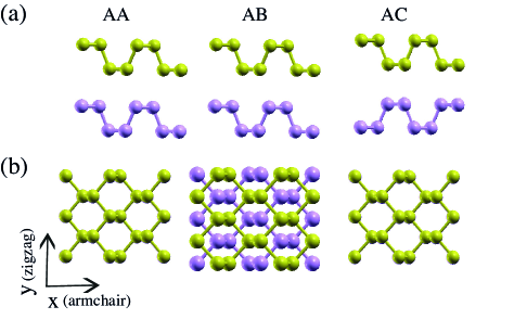
Bilayer phosphoren has been predicted to exist in three different stacking, namely AA, AB and AC structures (Fig.1). For the AA stacking, the top layer is directly stacked on the bottom layer. The AB stacking can be viewed as shifting the bottom layer of the AA stacking by half of the cell along either the or directions. For the AC stacking, the top and bottom layers are mirror images of each other. Regarding the trilayer phosphorene, three possible stacking types (AAB, ABA, and ACA) are considered.
The ground-state energy calculations, stemming from our numerical calculations, show that the AB-stacked and ABA-stacked structures are energetically the most preferred for bilayer and trilayer phosphorene, respectively. For bilayer phosphorene with the AB-stacked structure, the interlayer separation between the closest phosphorene atoms is Å while the in-plane lattice constants remain the same. Throughout this study, we perform calculations on the most stable AB-stacked form of the bilayer and ABA-stacked form of trilayer phosphorene systems.
II.2 Current-current response tensor
In this section, we consider independent electrons which live in a local crystal potential obtained by DFT and interact with the electromagnetic field described by the vector potential, . We pursue the procedure given in Novko2016 and thus the screened current-current response tensor can be calculated by solving the Dyson equation
| (1) |
where and are the noninteracting current-current response tensor and free-photon propagator, respectively. Our system contains slabs repeated periodically and is a periodic function along the direction. Also, the photon propagator has a long-range character that leads to the interactions between adjacent crystal slabs. Therefore, the screened contains the effects of the coupling between supercells. One of the best idea to solve this problem is to suppose that supercells are not repeated periodically along the direction and the system has just one crystal slab, which is restricted to the region . It denotes contains just one term in the direction and photon propagator couples only to the charge or current fluctuations in the region , even if it propagates interaction all over the space.
With this well-known method for 2D materials, although the periodicity is broken along the direction, it remains in the plane. Therefore, we can perform the Fourier transform of the Dyson equation (Eq. 1) in the plane and results are given by
| (2) |
where is the momentum transfer vector parallel to the plane and are 2D reciprocal lattice vectors. Also, the Fourier transformed free-photon propagator is given by Despoja2009
| (3) |
where
| (4) |
The directions of (TE) and (TM) polarized fields describe by and , where is the velocity of light, and the is the unit vector in the direction.
Since the integration in Eq. 2 is performed for , the current fluctuation created in the region can interact via photon propagator only with the current fluctuation within the region , even though the induced electromagnetic field spread over the whole space. This restriction guarantees that contains information about only the electromagnetic modes characteristic of the electronic system limited to the region .
The current-current response tensor can be obtained by solving the matrix Dyson equation that it is Fourier transformed by Eq. 2 in the direction
where
The noninteracting current-current response tensor can also be written as
| (7) |
where the current vertices are
| (8) |
and
is the normalized volume and is the Fermi-Dirac distribution at temperature . Notice that we define the three-dimensional vector and the wave function is expanded over the plane waves with coefficients which are obtained by solving the Kohn-Sham equations self-consistently.
We can use a useful relation between the optical absorption and current-current response tensor that was already thoroughly discussed in Rukelj . Now, we want to exploit the normalized absorption power per unit area which is given by
| (9) |
where the dynamical spectral function is
| (10) |
in which, the form factors are
| (11) |
By using the energy conservation law, the transmitted electromagnetic energy flux can be calculated by
| (12) |
where is the reflected energy flux and given by
| (13) |
Here, the amplitude of the reflected and waves are
where is the angle between wave vector and the normal vector of the system surface. The surface electromagnetic field propagator is defined by
| (15) |
At the end of this section, it is worth mentioning that the dielectric tensor and the conductivity tensor can be obtained with the current-current response. The first one is defined as Despoja2011
| (16) |
which describes the response of phosphorene to an external homogeneous electrical field. With knowledge of the optical dielectric function, the refractive index of the system can be obtained. Moreover, the real part of the dielectric function describes the imaginary part of the optical conductivity, however, the imaginary part of the dielectric function describes the absorption of light.
Since , the longitudinal conductivity is given by
| (17) |
which corresponds to the experimentally measurable optical conductivity Novko2016 . The optical longitudinal conductivity includes the interband transitions and the contribution of the intraband transitions, which leads to the fact that the Drude-like term is no longer relevant in this study since the momentum relaxation time is assumed to be infinite. This approximation is valid at low temperature and for a clean sample where defect, impurity, and phonon scattering mechanisms are ignorable.
III NUMERICAL RESULTS AND DISCUSSIONS
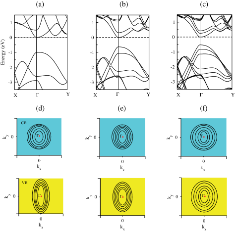
In this section, we present our numerical results for few-layer black phosphorus, based on first principles simulations within the DFT-RPA approach at zero temperature. The band structure of few-layer phosphorene is plotted in Fig. 2. Clearly, the band characteristic of the AB bilayer and ABA trilayer phosphorene are similar to that of the monolayer one, except that in the bilayer and trilayer, energy level splitting occurs due to the interlayer interactions. Our DFT calculations predict that the band gap of monolayer phosphorene is direct and equal to 0.98 eV and intriguingly, it decreases to 0.6 and 0.52 eV for bilayer and trilayer phosphorene, respectively. The nature of the band gap remains direct for trilayer to single-layer black phosphorous irrespective of the nature of stacking and it is more promising in terms of applying tunnel field-effect transistor devices Sengupta .
In the 2D case, the isofrequency profiles are obtained by horizontally cutting the dispersion surface. Also, the isofrequency contour plots of the energies around the conduction band minimum (CBM) and the valence band maximum (VBM) in the space of few-layer phosphorene are illustrated in Figs. 2(d) - 2(f). Most importantly, the shape of the Fermi surfaces in the systems is almost an elliptic shape, especially at low charge density. The elliptic shape of the Fermi surfaces, particularly in the hole-doped case demonstrates the anisotropic band energy dispersion of the few-layer phosphorene along the and directions. It turns out that, in the hole-doped cases, the anisotropic band energy dispersion decreases by increasing the number of the layers.
It is well-known that DFT underestimates the band gap of semiconductors and the advance Green’s function method can provide improved predictions. The Green’s function gap of monolayer phosphorene calculated by Tran et al. Tran2014 is about 2.0 eV. A recent Monte Carlo study of monolayer phosphorene Frank , using infinite periodic superlattices as well as finite clusters, predicted that the band gap is 2.4 eV.
III.1 Optical absorption and transmission of bilayer phosphorene
We explore the optical absorption calculated by using Eqs. 9-11 with the current-current response tensor (Eq. 7) . Having calculated the structure of few-layer phosphorene, we can obtain the Kohn-Sham wave functions and energies which are invoked to calculate the current-current response, . In the summation over in Eq. 7, we use -point mesh sampling and band summation (, ) is performed over and bands for bilayer and trilayer phosphorene, respectively. The damping parameter, is meV in all figures, unless we specifically define this value otherwise.
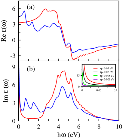
The real and imaginary parts of the ab initio DFT dielectric function (Eq. 16) are shown in Fig 3. The dielectric function is calculated by invoking the Kohn-Sham wave functions and they change by changing the structures and inter-atomic interactions. Therefore, the dielectric function depends on the material density and the interlayer distance.
We ought to note that at the onset of transparency at the plasmon frequency we have . The imaginary part of the DFT dielectric function shows the excitations in the system. The displays considerable structure before decreasing to become nearly zero at eV. This leads us to imagine that below 2 eV, is due to the topmost occupied electron levels. Electrons above 10 eV play no significant part in the optical spectrum. As shown in Fig. 3, the peaks in the imaginary part of the dielectric function are located in the energy range between and eV, where the absorptions are maximum, which corresponds to the drop of the real part of the dielectric functions. The values of the extremum positions for both imaginary and real parts of the dielectric function are equal as they are related by the Kramers-Kroning relations. It is worth to mention that the finite values of around are a numerical artifact and it should be zero. This artifact is related to the finite value of , and from factor in Eq. 16 and it can be reduced by decreasing of Sangalli . In the inset of Fig. 3(b), we illustrate the imaginary part of for different values of . The role of in this problem is completely clear.
There is an important -sum rule for the dielectric function which is used in the analysis of the absorption spectral. A general -sum rule for the imaginary part of the dielectric function says that
| (18) |
where is the number of electrons, is the unit cell volume and is the electron bare mass. We validate our numerical DFT-RPA results by considering 200 band structures in each system and find that the theory gives satisfactory results by 6%.
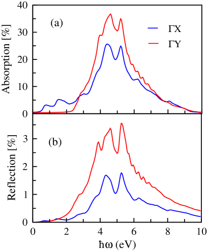
The optical absorption and reflection of the and -polarized normal incidence () are shown in Fig. 4 as a function of photon energy () for bilayer phosphorene. The optical absorption illustrates a maximum around energy between eV where the most profound photon-induced absorption of electrons between the mentioned bands occurs. The optical transition of the valence band to the conduction band appears along the armchair direction at about eV, while it is zero between and eV along the zigzag direction. This phenomenon originates from the contribution of in this region and consistent with experimental observations reported in Ref. Buscema . These results demonstrate a strong linear dichroism in bilayer phosphorene, where the position of the lowest energy absorption peaks for the armchair and zigzag directions differ significantly.
It can be found from the symmetry of the wavefunctions that dipole operator connects the VBM and CBM states for the -polarization, allowing the direct-band gap process, however, this is symmetry-forbidden for the -polarization and transition occurs between the VBM and CBM states elsewhere in the Brillouin zone qiao . Therefore, we expect that phosphorene would be a suitable material for applications associated with liquid-crystal displays and optical quantum computers knill ; zeng .
It should be noted that the reflection part of the incident light is negligible as shown in Fig. 4(b). Therefore, the main part of the optical properties goes to the transmission and absorption parts.
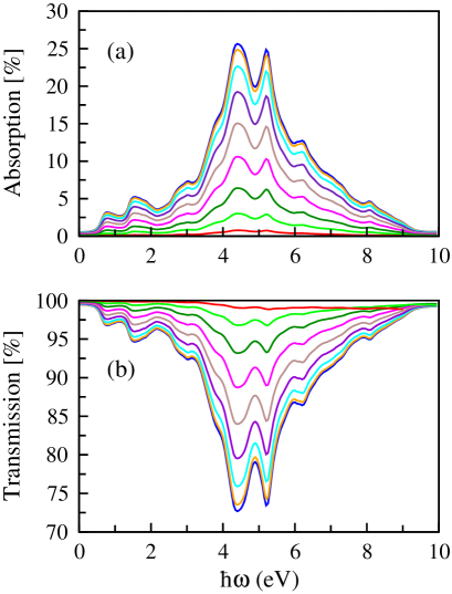
We also analyze the optical absorption and transmission of bilayer phosphorene as functions of the incident angle and photon energy along the armchair direction (Fig. 5). It is observed that the optical absorbance monotonically decreases, as the incident angle of light increases, however, the transmission increases. In particular, Fig. 5 shows that bilayer phosphorene is transparent when it is illuminated by a nearly grazing incidence light. It is intriguing that the peaks in the absorption spectra correspond to the dips in the transmitted spectra and the peaks show that the reflected light is negligible. Similar physical behaviors have been obtained for few-layer phsophorene and monolayer MoS2 Rukelj .
We would like to recall well-known dipole selection rules, which determines whether transitions are alloweded or forbidden based on the symmetry of the valence or conduction wave functions. The optical absorption can be calculated in the dipole-transition approximation as Tran2015
| (19) |
where is the dipole matrix operator and is the direction of the polarization of the incident light. The dipole selection rules allow transitions in which angular momentum between the valence and the conduction states differ from unity. Since the parity of is odd, two wavefunctions of the valence and the conduction have opposite parities in the direction of and the same parity in other directions. It is worth mentioning that in order to have a significant absorption at a particular energy, the joint density of states, , must have a Van-Hove singularity for a given energy. Most importantly, this one-particle picture of the transition process is totally inadequate and does not come close to describing the absorption spectra observed in experiments. Consequently, our analysis based on the many-body optical absorption is needed.
Note that when states near the VBM or the CBM have multicomponent characters, the spinors describing these components can pick up nonzero winding numbers and in such systems, the strength and required light polarization of an excitonic optical transition are dictated by the optical matrix element winding number. This winding-number physics, which mainly emerge in nanoribbon structures, leads to novel exciton series and optical selection rules Cao2018 . In this work, we focus on only the sum-rule selection rules presented in Eq. 19.
For bilayer phosphorene, the percent contribution from each atomic orbital to the valence and the conduction wavefunctions at the special -point listed in Tabel. 1. The optical absorption edge along the armchair direction is related to an interband transition from the VBM to the CBM and the allowed transitions are , and .
For a zigzag polarization, on the other hand, the optical absorption edge around eV is from the VBM to CBM+1 (the next band higher in energy than the conduction band) at a point along the direction which mainly originates from the interband transition. In this case, CBM+1 contains components of and which it causes allowed transitions such as , and .
A similar analysis of the optical transition is applicable for the trilayer phosphorene based on the details given in Table I. 1.
| type | direction | (X,Y) | state | ||||||||||
|---|---|---|---|---|---|---|---|---|---|---|---|---|---|
| bilayer | armchair | (0,0) | CBM | 6 | 42 | 17 | 0 | 28 | 4 | 0 | 1 | 0 | |
| VBM | 8 | 72 | 4 | 0 | 0 | 10 | 0 | 5 | 0 | ||||
| bilayer | zigzag | (0,0.35) | CBM+1 | 2 | 24 | 6 | 21 | 1 | 7 | 3 | 6 | 26 | |
| VBM | 12 | 70 | 1 | 10 | 0 | 1 | 0 | 1 | 5 | ||||
| trilayer | armchair | (0,0) | CBM | 9 | 38 | 16 | 0 | 30 | 6 | 0 | 1 | 0 | |
| VBM | 7 | 77 | 3 | 0 | 0 | 5 | 0 | 5 | 0 | ||||
| trilayer | zigzag | (0,0.38) | CBM+1 | 5 | 7 | 19 | 24 | 3 | 6 | 3 | 6 | 26 | |
| VBM | 6 | 72 | 1 | 0 | 0 | 1 | 8 | 1 | 8 |
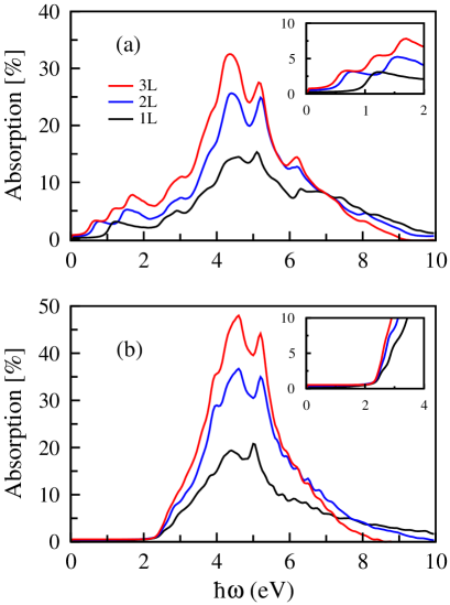
The optical absorption for the normal incidence () of light of a few-layer phosphorene along the armchair and zigzag directions are compared in Fig. 6. It can be noticed that the optical absorption spectra of the bilayer and trilayer are generally similar to that of the monolayer phosphorene. It is also noticeable that there is a general trend of an increase in the absorption by increasing the number of layers. This result shows that light absorptivity can be improved by appropriately increasing the number of layers in few-layer phosphorene Sengupta . In the low-energy zone, the absorption spectrum is red-shifted by increasing the number of the layers along the armchair direction, while it changes slightly with the addition of phosphorene’s layers along the zigzag direction.
This phenomenon originates from the decreasing of the energy band gap with increasing the number of the layers. The optical absorption edges are found to start approximately from the band gap. Therefore, the optical absorption edge can be tuned by changing of layers in few-layer phosphoren.
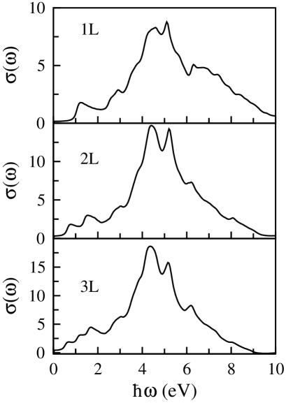
The optical conductivity of few-layer phosphorene is calculated by using Eq. 17. It is illustrated in Fig. 7 for , the homogeneous electrical field directed in the direction. It is clear there is no new feature regarding the optical conductivity in comparison with the absorption. As mentioned in Ref. Novko2016 , the unscreened () becomes equal to the screened () current-current response for , and is nonzero only for where the form factor eventually becomes a constant. Therefore, it can be concluded that the absorption becomes proportional to the optical conductivity.
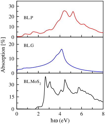
In Fig. 8, we compare the optical absorption of bilayer phosphorene with those of graphene and molybdenum disulfide for meV. As shown in the case of graphene, the absorption onset starts from eV which is due to the gapless dipole active to interband transitions near the point of the Brillouin zone. However, it is nearly zero in the region between eV for bilayer phosphorene and eV for bilayer MoS2. In fact, it shows semimetal nature in bilayer graphene and semiconductor characteristic of bilayer phosphorene and bilayer MoS2.
Regarding bilayer graphene, in the infrared region, the spectral absorption per pristine graphene layer is a constant, ( is the fine-structure constant), in good agreement with that obtained in a recent experiment and theoretical predictions Yang ; Nair . Obviously this value is valid for perfect graphene flake and depends strongly on the damping constant used in the calculation. In the visible energy, the absorption monotonically increases. The first absorption maximum, which appears in the ultraviolet region at eV, is a consequence of the dipole active interband to transitions along the MM’ and M directions of the first Brillouin zone, as discussed in details in Ref Novko_2015 .
Bilayer phosphorene exhibits greater absorbance compared to the optical absorption of AB bilayer graphene in the ultraviolet region. The same results pertain to their monolayer attribute Lin . Therefore, these results reveal that phosphorene absorb light strongly and it is a promising material to utilize in thin-film solar cells and photoelectric converters Dai_bi .
The onset of optical absorption in AB bilayer MoS2 is about eV and slowly increasing to a plateau, which corresponds to a transition of the valence band to the conduction band around the point. The intense peak is at 2.7 eV which is red-shifted compared to the intense peak in the monolayer. It is worth mentioning that the maximal peak of the absorption of bilayer MoS2 is in the visible region, while bilayer graphene and phosphorene are transparent in this region.
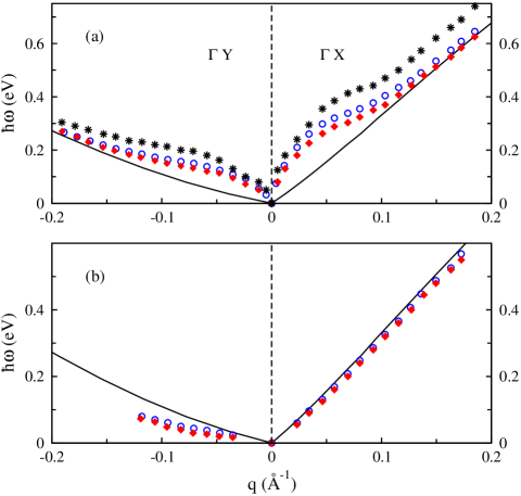
Finally, we use the formalism that was presented in previous works Novko_2015 ; torbatian ; torbatian2018 and calculate the collective modes of few-layer phosphorene. To do so, the Fermi energy is set to be eV above the edge of the conduction band of each phosphorene structure and our numerical results are illustrated in Fig. 9. One mode is the optical plasmon mode, which has its counterpart in single-layer samples with . This mode corresponds to a collective excitation of the electron gas in which the carriers of both layers oscillate in-phase. The optical plasmon modes increase by doping the system. Although both optical plasmon modes along the and directions follow a low-energy dependence Low , the plasmon in the armchair direction has a higher density than that the zigzag and armchair directions make the anisotropic plasmon mode in both two directions Rodin . Also, it can be seen that the optical plasmon mode of (monolayer) (bilayer) (trilayer). It is related to the electron concentration that those systems contain. Basically, with eV, the electron concentration of monolayer phosphorene is greater than that in the bilayer and thus the trilayer has the lowest electron concentration at given the Fermi energy. In addition to the optical mode, we observe the existence of an additional mode in the excitation spectrum dispersion for bilayer and trilayer phosphorene. In Fig. 9(b), the acoustic modes of bilayer and trilayer phosphorene along the and directions are shown. These modes correspond to a collective oscillation in which the carrier density in the two layers oscillates out-of-phase. These modes with a low-energy nearly linear dispersion are damped as they lie on the electron-hole continuum region.
IV CONCLUSION
In this work, we have analyzed the angle-resolved optical absorption and transmission of few-layer phosphorene using the current-current response tensor calculated in the framework of ab initio DFT calculations and the many-body random phase approximation. The optical transition of the valence band to the conduction band appears along the armchair direction at about 0.72 eV, while it is zero between 0 and 2.5 eV along the zigzag direction in bilayer phosphorene. In few-layer phosphorene, it is observed that the optical absorbance monotonically decreases, as the incident angle of light increases, and is transparent when it is illuminated by near grazing incidence of light. But the transmission increases, as the incident angle of light increases and it becomes almost for near grazing incidence. It can be noticed that the optical absorption spectra increases by increasing the number of layers. In the low-energy zone, the absorption spectrum is red-shifted by increasing the number of layers along the armchair direction, while it changes slightly along the zigzag direction. Also, we have compared the optical absorption of bilayer phosphorene with those of bilayer graphene and MoS2. It is shown that the bilayer phosphorene exhibits greater absorbance than the optical absorption of bilayer graphene in the ultraviolet region. The maximal peak in the absorption of bilayer MoS2 is in the visible region, while bilayer graphene and phosphorene are transparent in this region. Moreover, the anisotropy of the band structure of few-layer phosphorene along the armchair and zigzag directions is manifested in the collective plasmon excitations. Our results provide a microscopic understanding of the electronic and optical characteristics of few-layer phosphorene.
V acknowledgments
We thank H. Akbarzadeh for fruitful discussions and his help. Z. T. would like to thank the Iran National Science Foundation for its support. This work is also supported by the Iran Science Elites Federation.
References
- (1) Y. B. Zhang, Y. W. Tan, H. L. Stormer, and P. Kim, Nature. 438 , 201 (2005).
- (2) M. B. Lundeberg, Y. Gao, R. Asgari, C. Tan, B. Van Duppen, M. Autore, P. Alonso-Gonzalez, A. Woessner, K. Watanabe, T. Taniguchi, R. Hillenbrand, J. Hone, M. Polini, F. H.L. Koppens Science 357 187 (2017).
- (3) Q. H. Wang, K. Kalantar-Zadeh, A. Kis, J. N. Coleman, and M. S. Strano, Nature Nanotech. 7 , 699 (2012).
- (4) V. Wang, Y. Kawazoe, and W. T. Geng, Phys. Rev. B 91, 045433 (2015).
- (5) Q. Liu, X. Zhang, L. B. Abdalla, A. Fazzio and A. Zunger. Nano Lett. 15 1222(2015).
- (6) J. Qiao, X. Kong, Z. X. Hu, F. Yang and W. Ji Nature Commun. 5, 4475 (2014).
- (7) X. Peng, Q. Wei and A. Copple Phys. Rev. B 90, 085402 (2014).
- (8) D. Warschauer, J. Appl. Phys. 34 1853 (1963).
- (9) F. Xia, H. Wang and Y. Jia, Nat. Commun. 5 4458 (2014).
- (10) J. Lu, J. Yang, A. Carvalho, H. Liu, Y. Lu and C. H. Sow. Acc. Chem. Res. 49(9), 1806-1815 (2016).
- (11) G. Wang, R. Pandey, and S. P. Karna, Nanoscale 7 , 524 (2015).
- (12) Z. Jin, J. T. Mullen and K. W. Kim, Appl. Phys. Lett. 109, 053108 (2016).
- (13) M. Zare, B. Z. Rameshti, F. G. Ghamsari, and R. Asgari, Phys. Rev. B 95, 045422 (2017).
- (14) Z. Nourbakhsh, and R. Asgari, Phys. Rev. B 94 , 035437 (2016).
- (15) T. Zhang, J.-H. Lin, Y.-M. Yu, X.-R. Chen, and W.-M. Liu, Sci. Rep. 513927 (2015).
- (16) V. Tran, R. Soklaski, Y. Liang, L. Yang, Phys. Rev. B 89 235319(2014).
- (17) J. Dai and X. C. Zeng, J. Phys. Chem. Lett. 5 1289 (2014).
- (18) M. Buscema, D. J. Groenendijk, S. I. Blanter, G. A. Steele, H. S. J. van der Zant, and A. Castellanos-Gomez, Nano Lett., 14, 3347 (2014).
- (19) V. Tran and L. Yang, Phys. Rev. B 89, 245407 (2014)
- (20) D. Novko, M. Šunjić and V. Despoja, Phys. Rev. B 93, 125413 (2016).
- (21) D. Novko, V. Despoja, and M. Šunjić, Phys. Rev. B 91, 195407 (2015).
- (22) Z. Torbatian and R. Asgari J. Physics: Condens. Matter 29, 465701 (2017).
- (23) Z. Torbatian and R. Asgari Appl. Sci. 8, 238 (2018).
- (24) P. Giannozzi, S. Baroni, N. Bonini, M. Calandra, R. Car, C. Cavazzoni, D. Ceresoli, G. L. Chiarotti, M. Cococcioni, I. Dabo et al., J. Phys.: Condens. Matter 21, 395502 (2009).
- (25) J. P. Perdew, K. Burke, and M. Ernzerhof, Phys. Rev. Lett. 77, 3865 (1996).
- (26) M. Elahi, K. Khaliji, S. M. Tabatabaei, M. Pourfath, and R. Asgari, Phys. Rev. B 91, 115412 (2015).
- (27) V. Despoja, M. Šunjić and L. Marušić, Phys. Rev. B 80, 075410 (2009).
- (28) Z. Rukelj, A. Strkalj and V. Despoja, Phys. Rev. B 94, 115428 (2016).
- (29) V. Despoja, M. Šunjić and L. Marušić, Phys. Rev. B 83, 165421 (2011).
- (30) A. Sengupta, M. Audiffred, T. Heine and T. A. Niehaus, J. Phys.: Condens. Matter 28, 075001 (2016).
- (31) T. Frank, R. Derian, K. Tokar, L. Mitas, J. Fabian and I. Stich, arXiv: 1805.10823.
- (32) D. Sangalli, J. A. Berger, C. Attaccalite, M. Grüning and Pina Romaniello Phys. Rev. B 95, 155203 (2017).
- (33) A. Knill, R. Laflamme, G. J. Milburn, Nature (London) 409,46 (2001).
- (34) N. Zeng, X. Jiang, Q. Gao, Y. He, and H. Ma, Appl. Opt. 48, 6734 (2009).
- (35) V. Tran, R. Fei, and L. Yang 2D Mater.2, 044014 (2015).
- (36) T. Cao, M. Wu, and S. G. Louie, Phys. Rev. Lett. 120, 087402 (2018).
- (37) L. Yang, J. Deslippe, C. H. Park, M. L. Cohen, and S. G. Louie, Phys. Rev. Lett 103, 186802 (2009).
- (38) R. R. Nair, P. Blake, A. N. Grigorenko, K. S. Novoselov, T. J. Booth, T. Stauber, N. M. R. Peres, and A. K. Geim Science 320, 1308 (2008).
- (39) J.-H. Lin, H. Zhang and X. -L. Cheng, Front. Phys. 10, 107301 (2015).
- (40) T. Low, R. Roldán, H. Wang, F. Xia, P. Avouris, L. M. Moreno and F. Guinea, Phys. Rev. Lett 113, 106802 (2014).
- (41) A. S. Rodin and A. H. Castro Neto, Phys. Rev. B 91, 075422 (2015).