New generation of moiré superlattices in doubly aligned hBN/graphene/hBN heterostructures
Abstract
The specific rotational alignment of two-dimensional lattices results in a moiré superlattice with a larger period than the original lattices and allows one to engineer the electronic band structure of such materials. So far, transport signatures of such superlattices have been reported for graphene/hBN and graphene/graphene systems. Here we report moiré superlattices in fully hBN encapsulated graphene with both the top and the bottom hBN aligned to the graphene. In the graphene, two different moiré superlattices form with the top and the bottom hBN, respectively. The overlay of the two superlattices can result in a third superlattice with a period larger than the maximum period () in the graphene/hBN system, which we explain in a simple model. This new type of band structure engineering allows one to artificially create an even wider spectrum of electronic properties in two-dimensional materials.
Superlattice (SL) structures have been used to engineer electronic properties of two-dimensional electron systems for decades Weiss et al. (1989, 1991); Pfannkuche and Gerhardts (1992); Ferry (1992); Schlösser et al. (1996); Albrecht et al. (1999, 2001); Geisler et al. (2004). Due to the peculiar electronic properties of graphene Castro Neto et al. (2009), SLs in graphene are of particular interest Park et al. (2008a, b); Barbier et al. (2008); Brey and Fertig (2009); Sun et al. (2010); Burset et al. (2011); Ortix et al. (2012) and have been investigated extensively utilizing different approaches, such as electrostatic gating Dubey et al. (2013); Drienovsky et al. (2014, 2018), chemical doping Sun et al. (2011), etching Bai et al. (2010); Sandner et al. (2015); Yagi et al. (2015), lattice deformation Zhang et al. (2018) and surface dielectric patterning Forsythe et al. (2018). Since the introduction of hexagonal boron nitride (hBN) as a substrate for graphene electronics Dean et al. (2010), moiré superlattices (MSLs) originating from the rotational alignment of the two lattices have been first observed and studied by STM Decker et al. (2011); Xue et al. (2011); Yankowitz et al. (2012). It then triggered many theoretical Kindermann et al. (2012); Wallbank et al. (2013); Song et al. (2013); Moon and Koshino (2014) and experimental studies, where secondary Dirac points Ponomarenko et al. (2013); Dean et al. (2013); Hunt et al. (2013), the Hofstadter Butterfly Ponomarenko et al. (2013); Dean et al. (2013); Hunt et al. (2013); Yu et al. (2014); Wang et al. (2015), Brown-Zak oscillations Ponomarenko et al. (2013); Krishna Kumar et al. (2017), the formation of valley polarized currents Gorbachev et al. (2014) and many other novel electronic device characteristics Woods et al. (2014); Shi et al. (2014); Lee et al. (2016); Wang et al. (2016); Handschin et al. (2017); Spanton et al. (2018) have been observed.
Recently, another interesting graphene MSL system has drawn considerable attention – twisted bilayer graphene, where two monolayer graphene sheets are stacked on top of each other with a controlled twist angle. For small twist angles, insulating states Cao et al. (2016), strong correlations Kim et al. (2017) and a network of topological channels Rickhaus et al. (2018) have been reported experimentally. More strikingly, unconventional superconductivity Cao et al. (2018a); Yankowitz et al. (2018) and Mott-like insulator states Cao et al. (2018b); Yankowitz et al. (2018) have been achieved, when the twist angle is tuned to the so-called “magic angle”, where the electronic band structure near zero Fermi energy becomes flat, due to the strong interlayer coupling.
So far, MSL engineering in graphene has concentrated mostly on MSLs based on two relevant layers (2L-MSLs). However, graphene necessarily forms two interfaces, namely at the top and at the bottom, which can result in a much richer and more flexible tailoring of the graphene band structure. Due to the 1.8% larger lattice constant of hBN, the largest possible moiré period that can be achieved in graphene/hBN systems is limited to about Yankowitz et al. (2012), which occurs when the two layers are fully aligned. This situation changes when both hBN layers are aligned to the graphene layer. Here, we report the observation of a new MSL which can be understood by the overlay of two 2L-MSLs that form between the graphene monolayer and the top and bottom hBN layers of the encapsulation stack, respectively. Figure 1 illustrates the formation of the MSLs when both hBN layers are considered. On the right side of the illustration, only the top hBN (blue) and the graphene (black) are present, which form the top 2L-MSL with period . The bottom hBN (red) forms the bottom 2L-MSL with graphene, shown on the left with period . In the middle of the illustration all three layers are present and a new MSL (3L-MSL) forms with a longer period, indicated with . The influence of the MSL can be modeled as an effective periodic potential with the same symmetry. The periodic potentials for the top 2L-MSL and the bottom 2L-MSL are calculated following the model introduced in Ref Yankowitz et al. (2012), shown as insets in Fig. 1. To calculate the potentials for the 3L-MSL, we sum over the periodic potentials of the top 2L-MSL and the bottom 2L-MSL. The period of the 3L-MSL from the potential calculation matches very well the one of the lattice structure in the illustration. In the transport measurements, we demonstrate that MSL with a period longer than can indeed be obtained in doubly aligned hBN/graphene/hBN heterostructures, coexisting with the graphene/hBN 2L-MSLs. These experiments are in good agreement with a simple model for the moiré periods for doubly aligned hBN/graphene/hBN devices.
We fabricated fully encapsulated graphene devices with both the top and the bottom hBN layers aligned to the graphene using a dry-transfer method Wang et al. (2013). We estimate an alignment precision of . A global metallic bottom gate is used to tune the charge carrier density , and one-dimensional Cr/Au edge contacts are used to contact the graphene Wang et al. (2013) (see inset of Fig. 2(a)). Transport measurements were performed at using standard low-frequency lock-in techniques.
The two-terminal differential conductance, , of one device, shown as inset of Fig. 2(c), is plotted as a function of in Fig. 2(a) (data from other devices with similar characteristics, including bilayer graphene devices, are presented in the Supporting Information). The charge carrier density is calculated from the gate voltage using a parallel plate capacitor model. The average conductance is lower on the hole side () than on the electron side (), which we attribute to n-type contact doping resulting in a p-n junction near the contacts. The sharp dip in conductance at is the main Dirac point (MDP) of the pristine graphene. Our device shows a large field-effect mobility of , extracted from a linear fit around the MDP. The residual doping is of the order , extracted from the width of the MDP. In addition to the MDP, we find two pairs of conductance minima symmetrically around the MDP at higher doping, labeled A and C, which we attribute to two MSLs. The minima on the hole side are more pronounced than their counterparts on the electron side, similar to previously reported MSLs Yankowitz et al. (2012); Ponomarenko et al. (2013); Dean et al. (2013); Hunt et al. (2013).
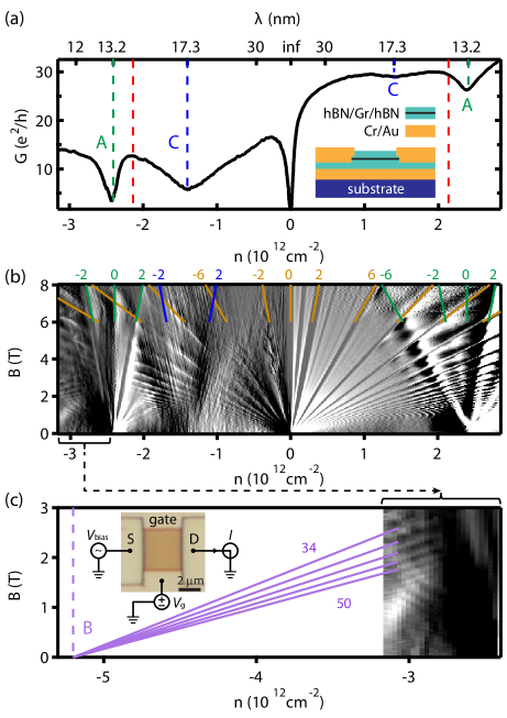
Superlattice Dirac points (SDPs) are expected to form at the superlattice Brillouin zone boundaries at , where is the length of the superlattice wavevector and the moiré period Park et al. (2008b). For graphene, is related to by . The position of the SDPs in charge carrier density for a given period is then . The pair of conductance minima at can be explained by a graphene/hBN 2L-MSL with a period of about . However, the pair of conductance minima at cannot be explained by a single graphene/hBN 2L-MSL, since it corresponds to a superlattice period of about , clearly larger than the maximum period of in a graphene/hBN moiré system. We attribute the presence of the conductance dips at to a new MSL that is formed by the three layers together: top hBN, graphene and bottom hBN. This 3L-MSL can have a period considerably larger than .
To substantiate this claim, we now analyse the data obtained in the quantum Hall regime. Figure 2(b) shows the Landau fan of the same device, where the numerical derivative of the conductance with respect to is plotted as a function of and the out-of-plane magnetic field . Near the MDP, we observe the standard quantum Hall effect for graphene with plateaus at filling factors , with the Planck constant and the electron charge. This spectrum shows the basic Dirac nature of the charge carriers in graphene. The broken symmetry states occur for , suggesting a high device quality. Around the SDPs at , the plot also shows filling factors , consistent with previous graphene/hBN MSL studies Ponomarenko et al. (2013). Around the SDPs at , there are also clear filling factors fanning out on the hole side with , which is consistent with a Dirac spectrum at , while on the electron side the corresponding features are too weak to be observed. In addition, lines faning out from a SDP located at density are observed. A zoom-in is plotted in Fig. 2(c). The lines extrapolate to a density of about , denoted , with filling factors This density cannot be explained by the “tertiary” Dirac point occuring at the density of about , which comes from a Kekulé superstructure on top of the graphene/hBN MSL Chen et al. (2017). However, matches the SDP from a MSL with a period of about . We therefore attribute it to a 2L-MSL originating from the alignment of the second hBN layer to the graphene layer.
As derived in Ref Yankowitz et al. (2012); Moon and Koshino (2014), the period for a graphene/hBN MSL is given by
| (1) |
where () is the graphene lattice constant, (1.8%) is the lattice mismatch between hBN and graphene and (defined for to ) is the twist angle of hBN with respect to graphene. The moiré period is maximum at with a value of . This corresponds to the lowest carrier density of for the position of the SDPs (red dashed lines in Fig. 2(a)). The orientation of the MSL is described by the angle relative to the graphene lattice,
| (2) |
For the graphene/hBN system, one finds Yankowitz et al. (2012). These two equations describe the top 2L-MSL and the bottom 2L-MSL, as shown schematically in Fig. 1.
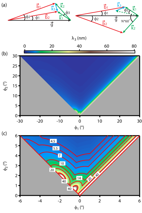
In a fully encapsulated graphene device, not only one, but both hBN layers can be aligned to the graphene layer so that two graphene/hBN 2L-MSLs can form. In this case, the potential modulations of the two 2L-MSLs are superimposed and form a MSL with a third periodicity. The values of the resulting periods can be understood based on Fig. 3(a). The vectors , and denote one of the reciprocal lattice vectors for the graphene, the top hBN and the bottom hBN layers, respectively. The twist angle between the top (bottom) hBN and graphene is denoted (). Following the derivations in Ref Yankowitz et al. (2012); Moon and Koshino (2014), one of the top 2L-MSL (bottom 2L-MSL) reciprocal lattice vectors () is given by the vector connecting to (). The moiré period is then given by , which is explicitly described by Eq. (1) as a function of the twist angle . Since the reciprocal lattices of the top 2L-MSL and the bottom 2L-MSL are triangular, the same as those for graphene and hBN, we can use the same approach to derive the 3L-MSL, which is described by the vector connecting to , denoted . The 3L-MSL period is then given by .
In order to calculate using Eq. (1), we first need to find the new , and . Due to symmetry, we only consider , so , the smaller period of the two graphene/hBN 2L-MSLs, becomes the new and the new will then be given by . The new , denoted , is determined by , where () is the relative orientation of the top 2L-MSL (bottom 2L-MSL) with respect to the graphene lattice, described by Eq. (2). Different cases occur for due to the rotational symmetry of the lattices. Since in Eq. (1) is defined for to , we subtract multiples of to bring to this range if it is larger than , given as
For the first case, the 3L-MSL is effectively the MSL formed by the two hBN layers, as illustrated in the left panel of Fig. 3(a). Another case is shown in the right panel, where multiples of are subtracted, which is equivalent to choosing another reciprocal lattice vector for so that it makes an angle within with .
Figure 3(b) plots all possible values for , as a function of and , by using Eq. (1) with the new parameters. Theoretically varies from below to infinity, but one finds values larger than only for small twist angles (see Fig. 3(c)). For most angles is very small, which explains why MSLs with periods larger than have not been reported in previous studies, where only one hBN layer was aligned intentionally to the graphene layer.
Most of Fig. 3(c) can be understood intuitively. On the line of the right diagonal with , we have and , therefore , which results in . This case is similar to the twisted bilayer graphene with a twist angle of 0, which does not form a MSL (or a MSL with infinitely large period). On the diagonal line in the left part with , one has , but . Therefore can have non-zero values, resulting in different values. This case is again similar to the twisted bilayer graphene, but with a tunable twist angle. The two maxima in occur if , , where is reset to 0 due to symmetry of the lattices, which is equivalent to the diagonal on the right part. The kinks on the contour lines come from the rotational symmetry of the lattices, where .
We now compare this simple model to our experiments. From the SDPs at , we calculate the corresponding moiré period and the twist angle . Similarly, for the extrapolated SDP at , we obtain and . The two twist angles give us two points in the map in Fig. 3(c): for (, ) and for (, ). The matches very well the value extracted from the new-generation SDPs at in the transport measurement, which confirms that the new-generation SDPs come from the 3L-MSL.
We fabricated five hBN/graphene/hBN heterostructures in total, two of which exhibit 3L-MSL features. Data from devices of the second heterostructure are presented in the Supporting Information, which has a 3L-MSL with .
In conclusion, we have demonstrated the emergence of a new generation of MSLs in fully encapsulated graphene devices with aligned top and bottom hBN layers. In these devices we find three different superlattice periods, one of which is larger than the maximum graphene/hBN moiré period, which we attribute to the combined top and bottom hBN potential modulation. Whereas our model describes qualitatively the densities where these 3L-MSL features occur, the precise nature of the band structure distortions is unknown. The alignment of both hBN layers to graphene opens new possibilities for graphene band structure engineering, therefore providing motivation for further studies. Our new approach of MSL engineering is not limited to graphene with hBN, but applies to two-dimensional materials in general, such as twisted trilayer graphene, graphene with transition metal dichalcogenides, etc., which might open a new direction in “twistronics” Carr et al. (2017); Ribeiro-Palau et al. (2018).
Acknowledgement
This work has received funding from the Swiss Nanoscience Institute (SNI), the ERC project TopSupra (787414), the European Union Horizon 2020 research and innovation programme under grant agreement No. 696656 (Graphene Flagship), the Swiss National Science Foundation, the Swiss NCCR QSIT, Topograph, ISpinText FlagERA network and from the OTKA FK-123894 grants. P.M. acknowledges support from the Bolyai Fellowship, the Marie Curie grant and the National Research, Development and Innovation Fund of Hungary within the Quantum Technology National Excellence Program (Project Nr. 2017-1.2.1-NKP-2017-00001). M.-H.L. acknowledges support from Taiwan Minister of Science and Technology (MOST) under Grant No. 107-2112-M-006-004-MY3. Growth of hexagonal boron nitride crystals was supported by the Elemental Strategy Initiative conducted by the MEXT, Japan and the CREST (JPMJCR15F3), JST. The authors thank David Indolese and Peter Rickhaus for fruitful discussions.
References
- Weiss et al. (1989) D. Weiss, K. V. Klitzing, K. Ploog, and G. Weimann, Europhys. Lett. 8, 179 (1989).
- Weiss et al. (1991) D. Weiss, M. L. Roukes, A. Menschig, P. Grambow, K. von Klitzing, and G. Weimann, Phys. Rev. Lett. 66, 2790 (1991).
- Pfannkuche and Gerhardts (1992) D. Pfannkuche and R. R. Gerhardts, Phys. Rev. B 46, 12606 (1992).
- Ferry (1992) D. Ferry, Prog. Quantum Electron. 16, 251 (1992).
- Schlösser et al. (1996) T. Schlösser, K. Ensslin, J. P. Kotthaus, and M. Holland, Europhys. Lett. 33, 683 (1996).
- Albrecht et al. (1999) C. Albrecht, J. H. Smet, D. Weiss, K. von Klitzing, R. Hennig, M. Langenbuch, M. Suhrke, U. Rössler, V. Umansky, and H. Schweizer, Phys. Rev. Lett. 83, 2234 (1999).
- Albrecht et al. (2001) C. Albrecht, J. H. Smet, K. von Klitzing, D. Weiss, V. Umansky, and H. Schweizer, Phys. Rev. Lett. 86, 147 (2001).
- Geisler et al. (2004) M. C. Geisler, J. H. Smet, V. Umansky, K. von Klitzing, B. Naundorf, R. Ketzmerick, and H. Schweizer, Phys. Rev. Lett. 92, 256801 (2004).
- Castro Neto et al. (2009) A. H. Castro Neto, F. Guinea, N. M. R. Peres, K. S. Novoselov, and A. K. Geim, Rev. Mod. Phys. 81, 109 (2009).
- Park et al. (2008a) C.-H. Park, L. Yang, Y.-W. Son, M. L. Cohen, and S. G. Louie, Nature Physics 4, 213 (2008a).
- Park et al. (2008b) C.-H. Park, L. Yang, Y.-W. Son, M. L. Cohen, and S. G. Louie, Phys. Rev. Lett. 101, 126804 (2008b).
- Barbier et al. (2008) M. Barbier, F. M. Peeters, P. Vasilopoulos, and J. M. Pereira, Phys. Rev. B 77, 115446 (2008).
- Brey and Fertig (2009) L. Brey and H. A. Fertig, Phys. Rev. Lett. 103, 046809 (2009).
- Sun et al. (2010) J. Sun, H. A. Fertig, and L. Brey, Phys. Rev. Lett. 105, 156801 (2010).
- Burset et al. (2011) P. Burset, A. L. Yeyati, L. Brey, and H. A. Fertig, Phys. Rev. B 83, 195434 (2011).
- Ortix et al. (2012) C. Ortix, L. Yang, and J. van den Brink, Phys. Rev. B 86, 081405 (2012).
- Dubey et al. (2013) S. Dubey, V. Singh, A. K. Bhat, P. Parikh, S. Grover, R. Sensarma, V. Tripathi, K. Sengupta, and M. M. Deshmukh, Nano Lett. 13, 3990 (2013).
- Drienovsky et al. (2014) M. Drienovsky, F.-X. Schrettenbrunner, A. Sandner, D. Weiss, J. Eroms, M.-H. Liu, F. Tkatschenko, and K. Richter, Phys. Rev. B 89, 115421 (2014).
- Drienovsky et al. (2018) M. Drienovsky, J. Joachimsmeyer, A. Sandner, M.-H. Liu, T. Taniguchi, K. Watanabe, K. Richter, D. Weiss, and J. Eroms, Phys. Rev. Lett. 121, 026806 (2018).
- Sun et al. (2011) Z. Sun, C. L. Pint, D. C. Marcano, C. Zhang, J. Yao, G. Ruan, Z. Yan, Y. Zhu, R. H. Hauge, and J. M. Tour, Nature Communications 2, 559 (2011).
- Bai et al. (2010) J. Bai, X. Zhong, S. Jiang, Y. Huang, and X. Duan, Nature Nanotechnology 5, 190 (2010).
- Sandner et al. (2015) A. Sandner, T. Preis, C. Schell, P. Giudici, K. Watanabe, T. Taniguchi, D. Weiss, and J. Eroms, Nano Lett. 15, 8402 (2015).
- Yagi et al. (2015) R. Yagi, R. Sakakibara, R. Ebisuoka, J. Onishi, K. Watanabe, T. Taniguchi, and Y. Iye, Phys. Rev. B 92, 195406 (2015).
- Zhang et al. (2018) Y. Zhang, Y. Kim, M. J. Gilbert, and N. Mason, npj 2D Materials and Applications 2, 31 (2018).
- Forsythe et al. (2018) C. Forsythe, X. Zhou, K. Watanabe, T. Taniguchi, A. Pasupathy, P. Moon, M. Koshino, P. Kim, and C. R. Dean, Nature Nanotechnology 13, 566 (2018).
- Dean et al. (2010) C. R. Dean, A. F. Young, I. Meric, C. Lee, L. Wang, S. Sorgenfrei, K. Watanabe, T. Taniguchi, P. Kim, K. L. Shepard, and J. Hone, Nature Nanotechnology 5, 722 (2010).
- Decker et al. (2011) R. Decker, Y. Wang, V. W. Brar, W. Regan, H.-Z. Tsai, Q. Wu, W. Gannett, A. Zettl, and M. F. Crommie, Nano Lett. 11, 2291 (2011).
- Xue et al. (2011) J. Xue, J. Sanchez-Yamagishi, D. Bulmash, P. Jacquod, A. Deshpande, K. Watanabe, T. Taniguchi, P. Jarillo-Herrero, and B. J. LeRoy, Nature Materials 10, 282 (2011).
- Yankowitz et al. (2012) M. Yankowitz, J. Xue, D. Cormode, J. D. Sanchez-Yamagishi, K. Watanabe, T. Taniguchi, P. Jarillo-Herrero, P. Jacquod, and B. J. LeRoy, Nature Physics 8, 382 (2012).
- Kindermann et al. (2012) M. Kindermann, B. Uchoa, and D. L. Miller, Phys. Rev. B 86, 115415 (2012).
- Wallbank et al. (2013) J. R. Wallbank, A. A. Patel, M. Mucha-Kruczyński, A. K. Geim, and V. I. Fal’ko, Phys. Rev. B 87, 245408 (2013).
- Song et al. (2013) J. C. W. Song, A. V. Shytov, and L. S. Levitov, Phys. Rev. Lett. 111, 266801 (2013).
- Moon and Koshino (2014) P. Moon and M. Koshino, Phys. Rev. B 90, 155406 (2014).
- Ponomarenko et al. (2013) L. A. Ponomarenko, R. V. Gorbachev, G. L. Yu, D. C. Elias, R. Jalil, A. A. Patel, A. Mishchenko, A. S. Mayorov, C. R. Woods, J. R. Wallbank, M. Mucha-Kruczynski, B. A. Piot, M. Potemski, I. V. Grigorieva, K. S. Novoselov, F. Guinea, V. I. Fal’ko, and A. K. Geim, Nature 497, 594 (2013).
- Dean et al. (2013) C. R. Dean, L. Wang, P. Maher, C. Forsythe, F. Ghahari, Y. Gao, J. Katoch, M. Ishigami, P. Moon, M. Koshino, T. Taniguchi, K. Watanabe, K. L. Shepard, J. Hone, and P. Kim, Nature 497, 598 (2013).
- Hunt et al. (2013) B. Hunt, J. D. Sanchez-Yamagishi, A. F. Young, M. Yankowitz, B. J. LeRoy, K. Watanabe, T. Taniguchi, P. Moon, M. Koshino, P. Jarillo-Herrero, and R. C. Ashoori, Science 340, 1427 (2013).
- Yu et al. (2014) G. L. Yu, R. V. Gorbachev, J. S. Tu, A. V. Kretinin, Y. Cao, R. Jalil, F. Withers, L. A. Ponomarenko, B. A. Piot, M. Potemski, D. C. Elias, X. Chen, K. Watanabe, T. Taniguchi, I. V. Grigorieva, K. S. Novoselov, V. I. Fal’ko, A. K. Geim, and A. Mishchenko, Nature Physics 10, 525 (2014).
- Wang et al. (2015) L. Wang, Y. Gao, B. Wen, Z. Han, T. Taniguchi, K. Watanabe, M. Koshino, J. Hone, and C. R. Dean, Science 350, 1231 (2015).
- Krishna Kumar et al. (2017) R. Krishna Kumar, X. Chen, G. H. Auton, A. Mishchenko, D. A. Bandurin, S. V. Morozov, Y. Cao, E. Khestanova, M. Ben Shalom, A. V. Kretinin, K. S. Novoselov, L. Eaves, I. V. Grigorieva, L. A. Ponomarenko, V. I. Fal’ko, and A. K. Geim, Science 357, 181 (2017).
- Gorbachev et al. (2014) R. V. Gorbachev, J. C. W. Song, G. L. Yu, A. V. Kretinin, F. Withers, Y. Cao, A. Mishchenko, I. V. Grigorieva, K. S. Novoselov, L. S. Levitov, and A. K. Geim, Science 346, 448 (2014).
- Woods et al. (2014) C. R. Woods, L. Britnell, A. Eckmann, R. S. Ma, J. C. Lu, H. M. Guo, X. Lin, G. L. Yu, Y. Cao, R. Gorbachev, A. V. Kretinin, J. Park, L. A. Ponomarenko, M. I. Katsnelson, Y. Gornostyrev, K. Watanabe, T. Taniguchi, C. Casiraghi, H.-J. Gao, A. K. Geim, and K. Novoselov, Nature Physics 10, 451 (2014).
- Shi et al. (2014) Z. Shi, C. Jin, W. Yang, L. Ju, J. Horng, X. Lu, H. A. Bechtel, M. C. Martin, D. Fu, J. Wu, K. Watanabe, T. Taniguchi, Y. Zhang, X. Bai, E. Wang, G. Zhang, and F. Wang, Nature Physics 10, 743 (2014).
- Lee et al. (2016) M. Lee, J. R. Wallbank, P. Gallagher, K. Watanabe, T. Taniguchi, V. I. Fal’ko, and D. Goldhaber-Gordon, Science 353, 1526 (2016).
- Wang et al. (2016) E. Wang, X. Lu, S. Ding, W. Yao, M. Yan, G. Wan, K. Deng, S. Wang, G. Chen, L. Ma, J. Jung, A. V. Fedorov, Y. Zhang, G. Zhang, and S. Zhou, Nature Physics 12, 1111 (2016).
- Handschin et al. (2017) C. Handschin, P. Makk, P. Rickhaus, M.-H. Liu, K. Watanabe, T. Taniguchi, K. Richter, and C. Schönenberger, Nano Lett. 17, 328 (2017).
- Spanton et al. (2018) E. M. Spanton, A. A. Zibrov, H. Zhou, T. Taniguchi, K. Watanabe, M. P. Zaletel, and A. F. Young, Science 360, 62 (2018).
- Cao et al. (2016) Y. Cao, J. Y. Luo, V. Fatemi, S. Fang, J. D. Sanchez-Yamagishi, K. Watanabe, T. Taniguchi, E. Kaxiras, and P. Jarillo-Herrero, Phys. Rev. Lett. 117, 116804 (2016).
- Kim et al. (2017) K. Kim, A. DaSilva, S. Huang, B. Fallahazad, S. Larentis, T. Taniguchi, K. Watanabe, B. J. LeRoy, A. H. MacDonald, and E. Tutuc, PNAS 114, 3364 (2017).
- Rickhaus et al. (2018) P. Rickhaus, J. Wallbank, S. Slizovskiy, R. Pisoni, H. Overweg, Y. Lee, M. Eich, M.-H. Liu, K. Watanabe, T. Taniguchi, T. Ihn, and K. Ensslin, Nano Lett. 18, 6725 (2018).
- Cao et al. (2018a) Y. Cao, V. Fatemi, S. Fang, K. Watanabe, T. Taniguchi, E. Kaxiras, and P. Jarillo-Herrero, Nature 556, 43 (2018a).
- Yankowitz et al. (2018) M. Yankowitz, S. Chen, H. Polshyn, K. Watanabe, T. Taniguchi, D. Graf, A. F. Young, and C. R. Dean, arXiv e-prints , arXiv:1808.07865 (2018), arXiv:1808.07865 .
- Cao et al. (2018b) Y. Cao, V. Fatemi, A. Demir, S. Fang, S. L. Tomarken, J. Y. Luo, J. D. Sanchez-Yamagishi, K. Watanabe, T. Taniguchi, E. Kaxiras, R. C. Ashoori, and P. Jarillo-Herrero, Nature 556, 80 (2018b).
- Wang et al. (2013) L. Wang, I. Meric, P. Y. Huang, Q. Gao, Y. Gao, H. Tran, T. Taniguchi, K. Watanabe, L. M. Campos, D. A. Muller, J. Guo, P. Kim, J. Hone, K. L. Shepard, and C. R. Dean, Science 342, 614 (2013).
- Chen et al. (2017) G. Chen, M. Sui, D. Wang, S. Wang, J. Jung, P. Moon, S. Adam, K. Watanabe, T. Taniguchi, S. Zhou, M. Koshino, G. Zhang, and Y. Zhang, Nano Lett. 17, 3576 (2017).
- Carr et al. (2017) S. Carr, D. Massatt, S. Fang, P. Cazeaux, M. Luskin, and E. Kaxiras, Phys. Rev. B 95, 075420 (2017).
- Ribeiro-Palau et al. (2018) R. Ribeiro-Palau, C. Zhang, K. Watanabe, T. Taniguchi, J. Hone, and C. R. Dean, Science 361, 690 (2018).