Fe-based superconducting thin films on metallic substrates: growth, characteristics and relevant properties
Abstract
The discovery of Fe-based superconductors (FBS) as the second class of high-temperature superconducting transition (high–) materials after the cuprates generated a significant impact on the community of fundamental and applied superconductivity research. Whenever a new class of high– superconducting materials is discovered, a lot of effort is devoted to growing single crystals and epitaxial thin films for exploring basic physical quantities. Although several properties of FBS are similar to the cuprates (large upper critical fields, as a consequence short coherence lengths, and small carrier density), others are distinctly different. For instance, in FBS the symmetry of the superconducting order parameter is most likely not a –wave but an –wave, depending on the stoichiometry, crystallographic system, and doping level. Additionally, the critical current densities of FBS are less sensitive to the presence of grain boundaries (GBs) than those of the high– cuprates. These features are highly beneficial for the realization of cheaper conductors for high-field magnets at low temperatures. Indeed, several groups have demonstrated FBS thin films on technical metallic substrates and powder-in-tube processed FBS wires as proof-of-principle studies for conductor applications. FBS on technical substrates also give many opportunities for studying how GB networks affect the critical current and how uniaxial strain impacts the superconducting properties. In this article, we review FBS thin films, especially on technical metallic substrates, and focus on application-relevant properties like pinning improvement by natural and artificial defects as well as the transparency of grain boundaries and GB networks. The recent development of FBS thin films on technical substrates and their superconducting properties are presented and the performance gap with respect to films on single crystals is discussed.
I Introduction
Since the first report of superconductivity in LaFeAs(O,F) 10 years ago by Hosono’s group,Kamihara et al. (2008) a lot of progress in the growth and synthesis of Fe-based superconducting (FBS) single crystals, bulks, wires, and thin films has been made. Now, high-quality thin films [e.g., FeSe, Fe(Se,Te), doped and undoped Fe2As2, where being an alkali earth element, and FeAs(O,F), where is a lanthanoide element, named respectively 11, 122 and 1111] are available on a large variety of single-crystalline and technical substrates. Hence fundamental as well as application-oriented research have been remarkably developed. In this article, we review FBS thin films, especially on technical metallic substrates, and focus on application-related properties like pinning improvement by natural and artificial defects as well as the transparency of grain boundaries (GBs) and GB networks. Many excellent review articles focussing on the growth of FBS thin films on single crystals and their physical properties have already been publishedLi, Si, and Dimitrov (2011); Hiramatsu et al. (2012a); Mele (2012); Haindl et al. (2014); Imai, Nabeshima, and Maeda (2017); Hosono et al. (2015, 2017); Sakoda, Iida, and Naito (2018) and the interested readers may also refer to them. The structure of this article is as follows: Naturally grown pinning centers are summarized, followed by artificial pinning centers. Afterwards, grain boundary experiments on Fe(Se,Te), doped BaFe2As2 (Ba-122) and NdFeAs(O,F) will be reviewed. Finally, FBS thin films on technical substrates will be described and discussed.
II Pinning improvements
| Materials | (K) | (T) | at | |||
|---|---|---|---|---|---|---|
| FeSeYang et al. (2017) | 8 | 72 | 0.55 | 16 | 0.04 | 0.3 at 4.2 K |
| Fe(Se0.5Te0.5)Klein et al. (2010) | 14 | 287 | 0.27 | 116 | 17.2 | 3.9 at 4.2 K |
| Co-doped Ba-122Yamamoto et al. (2009) | 22 | 66 | 0.5 | 38 | 0.1 | 0.2 at 4.2 K |
| P-doped Ba-122Chaparro et al. (2012) | 29 | 93 | 0.4 | 49 | 0.9 | 0.4 at 4.2 K |
| K-doped Ba-122Yang et al. (2017) | 38 | 80 | 0.5 | 180 | 0.1 | 0.6 at 20 K |
| NdFeAs(O,F)Kacmarcik et al. (2009) | 35 | 113 | 0.13 | 60 | 20.6 | 8.2 at 20 K |
| NdFeAs(O,F)Jaroszynski et al. (2008) | 47 | 87 | 0.11 | 162 | 6.5 | 3.4 at 20 K |
| YBCOYang et al. (2017) | 91 | 62 | 0.24 | 180 | 1.3 | 3.0 at 77 K |
| MgB2Zehetmayer et al. (2002) | 38 | 8 | 0.23 | 3 | 0.1 at 20 K |
One of the most important properties for wire and tape applications is the critical current density , which can be improved by microstructural engineering. Similar to the high– cuprates, the coherence length of FBS is in the order of a few nm.Putti et al. (2010) Hence nano-sized precipitates and defects can strongly pin the vortices in the mixed state. When transport currents flow in FBS in the mixed state, the Lorentz force acts on the vortices. If the pinning force is weaker than the Lorentz force, the vortices start to move, resulting in dissipation of energy. Hence the stronger the pinning force density, the higher the critical current density. Another effect which depins vortices is thermal fluctuations. This is quantified by the Ginzburg number () defined as the ratio of the minimal condensation energy within the coherence volume and the thermal energy at the critical temperature (, where is the Boltzmann constant). Thermal fluctuations are a serious problem for high– superconductors (HTS), for instance in YBa2Cu3O7 (YBCO) with a high of around 10-3 (table 1). For anisotropic superconductors, number in SI unit is evaluated by the following equation,Blatter et al. (1994)
| (1) |
where is the thermodynamic critical field at 0 K, is the upper critical field at 0 K, is the anisotropy parameter defined as , is the in-plane coherence length at 0 K, is the Ginzburg-Landau parameter at 0 K, and the right hand side is valid for basic SI units. It is noted that the is calculated by using the WHH formula. By using eq. (1), for various FBS is evaluated (table 1). Only for 122 and FeSe, is smaller than for YBCO and, therefore, the flux creep at the probable operating temperatures (minimum flux creep rate is expressed by Eley et al. (2017) due to thermal fluctuations is not a serious problem. Different is the case of the most anisotropic NdFeAs(O,F) and Fe(Se,Te) that could more strongly suffer from thermal fluctuations.
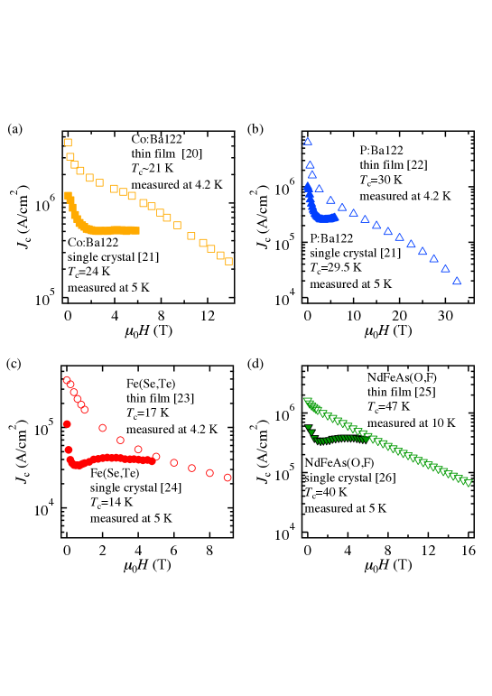
In general, thin films contain a higher density of natural defects than single crystals. In low magnetic fields, for thin films is higher than those for single crystals (fig. 1), whereas in high fields they appear to merge toward similar values. It is also noted that for single crystals has a non-monotonic field dependence due to the fish tail effect, whereas such an effect is absent in thin films. Considering the good performance already obtained in clean thin films, improvements in the in-field behavior are achievable by the introduction of artificial pinning centers with an appropriate control of their dimensionality (1D: columnar defects and dislocations, 2D: grain boundaries and anti-phase boundaries, and 3D: particlesMatsumoto and Mele (2010)) and their density.
In this section, the naturally grown pinning centers and artificial pinning centers in FBS are reviewed, and how these pinning centers influence the in-field is discussed.
II.1 Naturally grown pinning centers
II.1.1 Ba-Fe-O nanopillars
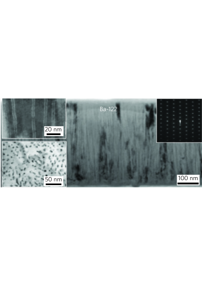
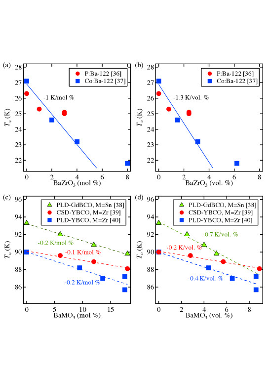
S. Lee . implemented SrTiO3 as buffer layer to grow epitaxial Co-doped Ba-122 on 001-oriented substrates ((LaAlO3)0.3(Sr2TaAlO6)0.7 (LSAT), GdScO3, LaAlO3 and Si) by pulsed laser deposition (PLD, KrF excimer laser).Lee et al. (2010) The nominal Co doping level of their PLD target was in Ba(Fe1-xCox)2As2 with a small As excess to compensate the loss of As during the deposition. They concluded that the use of a SrTiO3 template widened the range of possible substrates for high-quality Co-doped Ba-122 thin films. They also observed the formation of a high density of Ba-Fe-O nanopillars ( vol.%) that grew vertically from SrTiO3 to the film surface (fig. 2). As a result, the critical current density () for was higher than that for , which differs from what is expected by the mass anisotropy. The mean distance between nanopillars was 16-17 nm, which corresponds to a matching field of 7–8 T.Tarantini et al. (2010a) Indeed, the pinning force density showed a peak at around 8 T for . Later it was found that the oxygen content of the PLD targets strongly affects the Ba-Fe-O nanopillar density.Tarantini et al. (2012) Most importantly, this compound can accept a high density of Ba-Fe-O of up to 20 vol.% without compromising .
The detailed microstructural analysis by TEM identified the Ba-Fe-O phase as BaFeO2, which is an isostructure of tetragonal SrFeO2 (=0.3991 nm and =0.3474 nm).Zhang et al. (2011) The authors explained that BaFeO2 has nm due to a larger ionic radius of Ba compared to Sr and is coherently strained by the Ba-122 matrix.
II.1.2 Threading dislocations
-axis-correlated defects were also reported in Fe(Se,Te) thin films fabricated on SrTiO3 (001) substrates by PLD (KrF excimer laser) in Genova. In fig. 3, a high density of such defects with 2 nm diameter, comparable to the coherence length, was observed.Bellingeri et al. (2012) Bellingeri . speculated those defects were threading dislocations. Owing to these defects, for was higher than for at all temperatures, which is similar to the observation reported for nanopillars in Co-doped Ba-122.Lee et al. (2010) The mean defect separation was about 10 nm, corresponding to a matching field of 20 T. Consequently, for has a weaker field dependence than that for up to the maximum measured field of 9 T and in the temperature range below . The activation energy for vortex motion was raised by a factor 1.5 in these samples compared to a film on LaAlO3(100) substrate, where interestingly this kind of defects was absent.
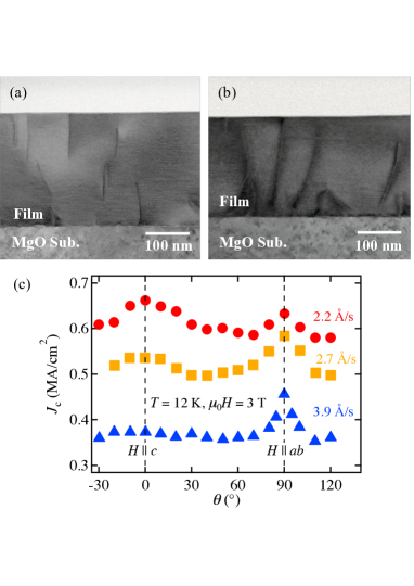
The introduction of threading dislocations in a controlled manner by tuning the growth conditions was reported for P-doped Ba-122 thin films by Sato .Sato et al. (2014) Shown in fig. 4(a) and (b) are the cross sectional views of two P-doped Ba-122 thin films grown on MgO substrates by PLD (Nd:YAG laser with 2nd harmonic) with different growth rates. Relatively short defects which are almost parallel to the Ba-122 -axis were observed for a growth rate of 2.2 Å/s and identified as threading dislocations (fig. 4(a)). On the other hand, tilted, long defects of relatively low density were seen for the film grown at 3.9 Å/s and identified as domain boundaries due to lateral growth (fig. 4(b)). The film grown at 2.2 Å/s with threading dislocations showed the highest in the full angular range among the films measured at 12 K and 3 T (fig. 4(c)).
II.1.3 Fe precipitates
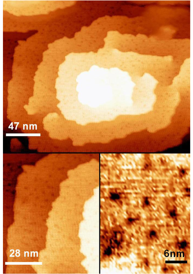
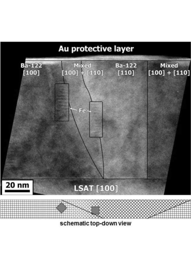
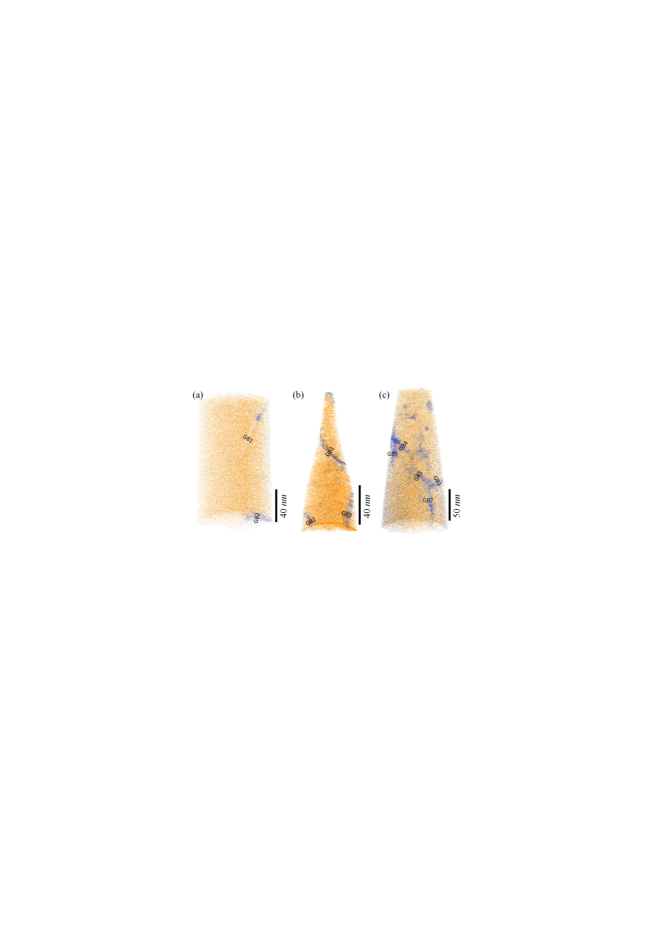
Hänisch . investigated Co-doped Ba-122 thin films containing 45∘ rotated grains grown by PLD (KrF excimer laser).Hänisch et al. (2014) They fabricated Co-doped Ba-122 thin films on LSAT(001) at a relatively low deposition temperature of 675∘C in ultra-high vacuum (UHV) condition. As a result, round and -axis elongated Fe precipitates were observed near or within the grain boundaries (fig. 5). These Fe particles, together with the threading dislocations in the GBs lead to a -axis peak in the anisotropy.
For P-doped Ba-122 thin films grown by molecular beam epitaxy (MBE), Sakagami . reported a maximum self-field of 10 MA/cm2 (4.2 K) for Fe-rich films () on MgO(001) substrates measured by a magnetization method.Sakagami et al. (2013) Although no microstructural investigations have been reported, the authors speculated two plausible reasons: one possibility is that nanoparticles of Fe or Fe-based compounds, which were not detectable by x-ray diffraction (XRD), are dispersed in the matrix of such Fe-rich P-doped Ba-122 films and act as pining centers. The other possibility is that an Fe layer is formed at the interface with the substrate and acts as a buffer layer that improves the crystallinity.
II.2 Artificial pinning centers
II.2.1 BaZrO3 nanoparticles in PLD-grown Co- and P-doped Ba-122
Using the same strategy for pinning enhancement of YBa2Cu3O7 films,MacManus-Driscoll et al. (2004) BaZrO3-added BaFe2(As1-xPx)2 Miura et al. (2013) and Ba(Fe1-xCox)2As2 Lee et al. (2017) sintered pellets were prepared by two groups for use as PLD targets. The former target was ablated by a 2nd harmonic Nd:YAG laser whereas the latter was ablated by a KrF excimer laser.
In P-doped Ba-122 films on MgO(001) substrate, nano-sized BaZrO3 particles with average diameter of 5–10 nm were finely distributed in the Ba-122 matrix.Miura et al. (2013) As a result, an almost isotropic of 1.5 MA/cm2 at 15 K () and 1 T was obtained. In Co-doped Ba-122 films on CaF2(001) substrate, short and -axis-oriented BaZrO3 nanorods with nm diameter, slightly larger than in YBCO (2 3 nm),Goyal et al. (2005) were formed in the Ba-122 matrix.Lee et al. (2017) The mean separation of BaZrO3 nanorods was 10–11 nm, corresponding to a matching field of 17–20 T. The optimized Co-doped Ba-122 with 2 mol% BaZrO3 showed an in-field of 1.3 MA/cm2 at 13 T and 4.2 K.
Figure 6 compares the reduction of in P-doped Ba-122 and Co-doped Ba-122. Up to 3 mol% (2.5 vol.%) of BaZrO3, the initial suppression rate of for both films is around -1 K/mol% (-1.3 K/vol.%), which is high compared to common values for GdBCO Chepikov et al. (2017) and YBCO Birlik et al. (2010); Horide et al. (2017). The difference in reduction against volume fraction is not as severe because of the smaller molar volume of the Ba-122 phase.
Compared to BaFeO2 nanopillars (see section Ba-Fe-O), the reduction of is significant, which may be ascribed to the different lattice mismatch.
II.2.2 Superlattices and multilayers
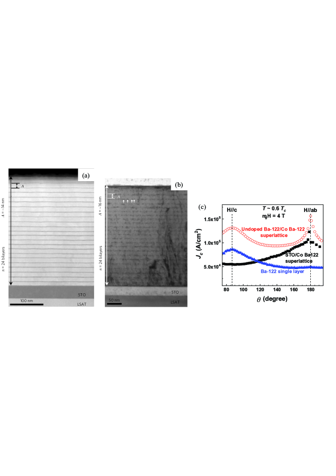
To date, FBS superlattices for Ba-122 Lee et al. (2013) and Fe(Se,Te) Nabeshima et al. (2017) have been reported by the Univ. Wisconsin and the Univ. of Tokyo, respectively. S. Lee . investigated the effect of SrTiO3 and undoped Ba-122 insertion layers on the structural and superconducting properties of Co-doped Ba-122 thin films. The cross-sectional TEM images of the (100) projection clearly showed the 24 bilayers of SrTiO3/Co-doped Ba-122 (fig. 7(a)). On the other hand, the insertion layer of undoped Ba-122 grew discontinuously in the lateral direction (fig. 7(b)). Similarly to the single layer reported by the same group, the undoped oxygen-rich Ba-122/Co-doped Ba-122 superlattice possessed vertical defects, presumably BaFeO2, which act as effective pinning centers along the crystallographic -direction. Combining the -axis and -planar pinning contributions improved in-field properties considerably, as shown in fig. 7(c).
Nabeshima . deposited FeSe/FeTe superlattices on CaF2 and LaAlO3.Nabeshima et al. (2017) From the microstructural investigations, some degree of Te/Se interdiffusion was observed. Because of the interdiffusion, the superconducting transition temperature of the FeSe/FeTe superlattice was improved compared to FeSe (i.e., from 12 K for FeSe on CaF2 to 15.8 K for FeSe/FeTe superlattice on CaF2). No information on critical current densities was reported on these films.
Besides introducing artificial pinning centers, the multilayer approach can improve the superconducting properties.Tarantini et al. (2014b); Engelmann et al. (2013); Chen et al. (2012) Tarantini . reported Co-doped, BaO-added Ba-122/Co-doped Ba-122 multilayer fabricated on CaF2(001) substrate for which the superconducting transition temperature was increased by compressive strain.Tarantini et al. (2014b) Pinning force densities as high as 84 and 70 GN/m3 for and at 4.2 K were achieved by a combination of short -axis nanorods, round nanoparticles and -arranged precipitates.
Engelmann . fabricated Co:Ba-122 (20 nm)/Fe (4 nm)/Co:Ba-122 (20 nm)/Fe (30 nm) multilayers on MgAl2O4, which showed a high of 29.4 K due probably to an As-deficiency.Engelmann et al. (2013) Chen . reported the enhancement of in-field performance for an Fe(Se,Te) double layer with a CeO2 insertion layer on SrTiO3.Chen et al. (2012) The improvement is ascribed to the additional interfacial defects introduced by the insertion layer.
II.2.3 Irradiation
| Materials | Particles | Total or Max. dose | Change in | Ref. |
|---|---|---|---|---|
| Fe(Se,Te) | Fast neutrons | -0.3 K | Eisterer et al.,2011 | |
| Fe(Se,Te) | 190 keV protons | +0.5 K | Ozaki et al.,2016 | |
| Fe(Se,Te) | 6 MeV Au | -0.5 K | Ozaki et al.,2018 | |
| Fe(Se,Te) | 3.5 MeV protons | -7.0 K | Ahmad et al.,2017 | |
| Fe(Se,Te) | 3.5 MeV protons | -0.6 K | Sylva et al.,2018 | |
| FeTe | 150 kV O | N.A. | Janaki et al.,2014 | |
| Co-doped Ba-122 | 3 MeV protons | -1.0 K | Maiorov et al.,2012 | |
| Co-doped Ba-122 | 200 keV protons | -18 K | Schilling et al.,2016 | |
| P-doped Ba-122 | 250 MeV Au | -0.8 K | Daghero et al.,2017 | |
| NdFeAs(O,F) | 2 MeV He | -3.0 K | Tarantini et al.,2018 |
Although many irradiation experiments on FBS single crystals have been reported, only few studies except for 11 report on the effects of irradiation in thin films (see table 2). An excellent review article on radiation effects in FBS has recently been published by Eisterer.Eisterer (2018) Here, we will briefly summarize the available data on FBS thin films.
The defects created by fast neutron irradiation on Fe(Se,Te) thin films produced only a small impact on the superconducting properties (, upper critical field, , irreversibility field, and ).Eisterer et al. (2011) On the other hand, low-energy proton irradiation created nanoscale compressive strain, resulting in an increase of by 0.5 K.Ozaki et al. (2016) Additionally, cascade defects combined with nanoscale strain worked as strong vortex pinning centers, and consequently increased by one order of magnitude at 12 K and by a factor of 2 at 4.2 K at fields around and above 15 T. Ozaki . also investigated the effect of Au irradiation on the superconducting properties of Fe(Se,Te) thin films.Ozaki et al. (2018) The Au-irradiated film showed a slight decrease in by 0.5 K. However, in-field properties were improved for all field orientations at 4.2 K. Furthermore, the enhancement was nearly 70% compared to the pristine film at 10 K and 9 T. Ahmad . reported the effect of proton irradiation effect on the superconducting properties of FeSe1-xTex (=0.4, 0.55) thin films.Ahmad et al. (2017) The reduction of superconducting properties caused by the local heating, which may accelerate the displacement of atoms and create vacancies. Sylva . pointed out the importance of the position where the proton is implanted: the improvement of up to 50% at 12 K and 7 T was observed when protons were accumulated far from the film/substrate interface. Simultaneously, and were unaltered.Sylva et al. (2018) On the other hand, superconducting properties were degraded when the proton implanted layer was close to the interface.
Non-superconducting FeTe thin films were irradiated by oxygen ions.Janaki et al. (2014) At the maximum dose of , the FeTe film was amorphous.
The effect of 3 MeV proton irradiation on the superconducting properties of Co-doped Ba-122 was reported by Maiorov .Maiorov et al. (2012) After the irradiation (total dose of cm-2), the decreased by only 1 K. Overall for the irradiated film was decreased in low field. At high field and low temperatures, was increased, particularly for () due to a clear anisotropic contribution from the point-like defects.
The effect of proton irradiation on Co-doped Ba-122 thin films was also reported by Schilling who investigated the disorder-induced symmetry change from to by THz spectroscopy.Schilling et al. (2016) On the assumption that the electron-electron coupling constant is positive, disorder induces a transition between to states.Efremov et al. (2011) In this report they observed such a transition: the small gap was closed at a certain amount of disorder and re-opened again by further increase of disorder. These results suggested that the superconducting order parameter in the pristine film has symmetry. However, no information on , and was reported.
Daghero reported on the effect of irradiation with 250-MeV Au ions on the superconducting properties of optimally P-doped Ba-122 thin films fabricated by MBE.Daghero et al. (2017) The residual resistivity at increased with dose level, whilst the decrease in was only 0.8 K for a maximum dose of . Such a small reduction in would indicate symmetry. The authors also considered the role of the substrate in the radiation effect: Au ion irradiation and heating in the substrate may have caused additional damage.
Unlike in NdFeAs(O,F) single crystals,Tarantini et al. (2010b) -particle irradiation on NdFeAs(O,F) thin films did not create Kondo-like defects,Tarantini et al. (2018) suggesting that the type of defects induced by this type of irradiation is also strongly affected by other factors, the most likely being the initial composition. In the irradiated NdFeAs(O,F) films an increase of both and were observed. However, only for a moderate improvement in was found, whereas for point-defects compete with intrinsic pinning, reducing .
III Grain boundaries
There are two main purposes for experiments on FBS thin films fabricated on bicrystal substrates having a single well-defined grain boundary. One is to realize Josephson junctions with two FBS electrodes for fundamental research and assessing potential of electronics application. The other goal is to check the transparency across the grain boundary, which is vital information for wire applications. In the former experiments, thin films are prepared on bicrystal substrates with relatively large misorientation angle to realize an SNS (superconductor–normal–superconductor) or SIS (superconductor–insulator–superconductor) junction. It is worth mentioning that all bicrystal experiments on FBS reported to date have been conducted using symmetric [001]-tilt bicrystal substrates (SrTiO3, MgO and LSAT). Hence grain boundary experiments using different types of bicrystals (i.e., valley- or roof-type [010]-tilt and [100]-twist) are necessary to obtain deeper knowledge of grain boundary characteristics of FBS, since inter-grain () depends in general on the GB type, as shown for YBa2Cu3O7 deposited on various types of bicrystals.Held et al. (2009) In general, different results are expected in case of different order parameter symmetry (e.g. –wave or –wave) as well as strain sensitivity and charge density.
To date, for FBS there have been only a few systematic and extended bicrystal experiments on Fe(Se,Te) and Co-doped Ba-122 films. Only singular experiments on P-doped Ba-122 Sakagami et al. (2013) and recently on NdFeAs(O,F) Omura et al. (2017) have been reported so far, table 3. Reviews on GB properties in FBS bulk and film samples in comparison to high- cuprate superconductors have been given by Deutscher in 2010 Deutscher (2010) and Durrell in 2011.Durrell et al. (2011) In the following subsections, we review all reported bicrystal experiments on FBS concerning Josephson junctions followed by inter-grain reduction due to weak-link behaviour. Some of the experiments mentioned below have been conducted for both purposes of Josephson junctions and investigation of the transparency across the grain boundary. Therefore, occasionally the same experiments are referred to in the subsections Josephson junctions with two FBS electrodes and Misorientation dependence of inter-grain .
| Materials | Deposition | Substrates | ||
|---|---|---|---|---|
| Fe(Se,Te) | PLD | SrTiO3 Sarnelli et al. (2014, 2017a, 2017b); Si et al. (2015) | 9∘ Si et al. (2015); Sarnelli et al. (2017a) | |
| Co-doped Ba-122 | PLD | SrTiO3 Lee et al. (2009); Schmidt et al. (2013) |
< 6∘ Lee et al. (2009)
|
|
| Co-doped Ba-122 | PLD | MgO Katase et al. (2013); Hiramatsu et al. (2012b); Iida et al. (2012), LSAT Katase et al. (2013); Hiramatsu et al. (2012b); Katase et al. (2010a, b) | 9∘ Katase et al. (2013); Hiramatsu et al. (2012b) | |
| P-doped Ba-122 | MBE | MgO Sakagami et al. (2013), LSAT Schmidt et al. (2014) | , | N.A. |
| NdFeAs(O,F) | MBE | MgO Omura et al. (2017) |
< 6∘
|
III.1 Josephson junctions with two FBS electrodes
III.1.1 Fe(Se,Te)
To date, four bicrystal experiments on Fe(Se,Te) have been published. First bicrystal experiments on Fe(Se,Te) were reported by Sarnelli who fabricated 150 nm thick Fe(Se,Te) films on [001]-tilt SrTiO3 bicrystals with a misorientation angle () of 45∘ by PLD using a Nd:YAG laser with a wave length of 1024 nm.Sarnelli et al. (2014) The authors made microbridges (2.6–20 m wide and 20 m long) on Fe(Se,Te) bicrystals by optical lithography and ion beam milling. To avoid possible damage during the process, the sample holder was cooled to -40∘C. The characteristics at 4.2 K showed a resistively shunted junction (RSJ) behavior with a low normal-state resistance in the range , which is typical for SNS junctions. Compared to the cuprates, those values are two orders of magnitude lower. As a result, the product was 1833 V, where is the Josephson critical current. Later, Sarnelli fabricated dc superconducting quantum interference devices (dc-SQUIDs) using 100-nm thick Fe(Se,Te) bicrystal with .Sarnelli et al. (2017a, b) The resultant device showed a clear voltage modulation under magnetic field with a maximum amplitude of 3.8 V at 4.2 K.
Si . fabricated 100-nm thick Fe(Se,Te) thin films on CeO2-buffered SrTiO3 bicrystal substrates (=4∘, 7∘, 15∘ and 24∘) by PLD.Si et al. (2015) Microbridges with 300 m length and 20–25 m width were fabricated by laser cutting for transport measurements. The curve of the bridge with showed a double superconducting transition at 20 K and 17.5 K with =0 at around 12 K. On the other hand, the bridge with had one transition at 20 K similar to the intra-grain bridge. Using the bridge with , the authors observed multiple Josephson current modulations by magnetic field. The magnitude of the modulation was around 80%. The characteristics at 2 K roughly followed the RSJ model with a normal state resistance of =28 m. Such a low value of is due to the metallic nature of the normal state of the Fe(Se,Te) bicrystal grain boundary junction. The product of their junctions was estimated to around 22 V at 2 K.
III.1.2 Co- and P-doped Ba-122
Katase reported on Josephson junctions and dc-SQUIDs in PLD-processed Co-doped Ba-122 (=21.5–22.6 K) using LSAT bicrystal substrates with .Katase et al. (2010a, b) For single Josephson junctions, the authors fabricated microbridges (10 m wide and 300 m long) by photolithography and Ar ion milling. The characteristics of the resultant junction at 4.2 K showed RSJ behavior. The normal state resistance of the junction was around 12 m, resulting in a low product of 50 V. For dc-SQUIDs, bridges with a smaller width of 3 m (area of SQUID loop was 188 m2) were made to reduce the critical current. The resultant device showed a clear voltage modulation with an amplitude of 1.4 V at 14 K. However, the shape of deviated from the ideal sinusoidal function. Additionally, the level of flux noise at 1 Hz was Hz-1/2, which was one order of magnitude higher than for cuprates. From those junction experiments, the barrier layer is of metallic nature in Co-doped Ba-122. Indeed, the inter-grain showed a quadratic temperature dependence, indicative of SNS rather than SIS junctions.Katase et al. (2013) Hence, for realizing practical SQUIDs it is necessary to increase the junction resistance by an artificial insulating barrier.
Schmidt . also reported on PLD-grown Co-doped Ba-122 grain boundary junctions using SrTiO3 with .Schmidt et al. (2013) To suppress oxygen diffusion from SrTiO3, a 10 nm thick MgAl2O4 layer was deposited on the SrTiO3 bicrystal. Fe-buffer layer followed by Co-doped Ba-122 were deposited on this template. All layers were epitaxially grown as confirmed by XRD. In their junctions (=24 K), a high excess current ( A) was observed, and therefore a small product of 6.5 V at 4.2 K was obtained.
Sakagami . prepared P-doped Ba-122 by MBE on [001]-tilt MgO bicrystals with .Sakagami et al. (2013) The characteristics of their device (=29.5 K, bridge width of 30 m) at 2 K was described by a flux-flow extension of the RSJ model, which gave a normal state resistance of =4.4 m and a Josephson critical current of =8.5 mA. As a consequence, a small product of 37 V was obtained. Such a low normal state resistance of the junction is due to the metallic nature of the grain boundary. The same group also fabricated P-doped Ba-122 thin films on LSAT bicrystals with Schmidt et al. (2014). The characteristics of the resultant junction can again be fitted by a RSJ model with flux flow current. Their device had an product of 45 V at 4.2 K. However, this value was corrected to 11 V by taking into account the excess current.
III.1.3 Summary of Josephson junctions with two FBS electrodes
All bicrystal junctions of Fe(Se,Te), Co-doped, and P-doped Ba-122 have the same low level of (tens of V) compared to that of YBCO (in the order of mV at 4.2 K). The main reason for such low is that the barrier layer is of metallic nature, which leads to a low junction resistance . Therefore, the dc-SQUIDs made from Fe(Se,Te) Sarnelli et al. (2017a) and Co-doped Ba-122 Katase et al. (2010b) showed high flux noise. The properties mentioned above are not suitable for electronics applications, however, are highly beneficial to wire applications. To realize electronics applications like SQUIDs, one would have to increase the by an artificial insulating barrier. Interested readers for Josephson effects in FBS may refer to Ref. Seidel, 2011.
III.2 Misorientation dependence of inter-grain
III.2.1 Fe(Se,Te)
The inter-grain of Fe(Se,Te) across a =45∘ grain boundary without magnetic field was around A/cm2 at 4.2 K, one order of magnitude lower than the intra-grain ().Sarnelli et al. (2014) These results suggested that the decay of with GB angle may not be as strong as for the cuprates, where at this angle the suppression is significant (4 orders of magnitude). Later, Sarnelli . have reported as a function of .Sarnelli et al. (2017a) It was found that the dependence of is almost similar to the result reported by Si .Si et al. (2015) Additionally, the level of was almost constant for and , which will be discussed later.
Si found that for and 7∘ maintained A/cm2 even in the presence of large applied magnetic fields (, ) at 4.2 K, indicative of strong links in this range.Si et al. (2015) On the other hand, for was significantly suppressed by a small magnetic field: for , e.g., was reduced from to A/cm2 even by a small magnetic field of . Based on the experimental results above, the authors concluded that the critical angle was around 9∘.
III.2.2 Co- and P-doped Ba-122
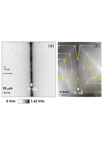
Already in the early stage of thin film research of pnictide superconductors, S. Lee reported on the weak-link behavior of [001] tilt GBs in Co-doped Ba-122.Lee et al. (2009) They fabricated 350-nm thick films ( over 20 K) on SrTiO3 bicrystals ( and 24∘) by PLD. Low-temperature laser scanning microscopy (LTLSM) and magneto-optical imaging (MOI) on these Co-doped Ba-122 bicrystal junctions with and 9∘ revealed the weak-link behavior also for low-angle GBs (fig. 8). As can be seen in fig. 8(a), a large dissipation across the 6∘ grain boundary was detected by LTLSM. For the 9∘ grain boundary sample, two clear roof-top shapes separated by the grain boundary are observed by MOI (fig. 8(b)). These results indicated that the critical angle may be below 6∘, which differs from results reported two years later by Katase .Katase et al. (2013) We speculate that oxygen impurities may have limited the for these Co-doped Ba-122 films on SrTiO3. In fact, it is likely that the nanorods (see subsection BaFeO3 nanopillars) tend to segregate along the GB reducing the effective cross-section and consequently . Detailed microstructural investigations are necessary to identify such differences.
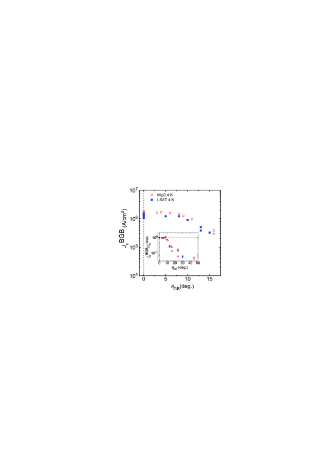
Later Katase, Hiramatsu reported a as large as 9∘ from their detailed bicrystal experiments on Co-doped Ba-122.Katase et al. (2013); Hiramatsu et al. (2012b) Here the respective of Co-doped Ba-122 were 20.7 K on MgO and 21.6 K on LSAT bicrystals. Shown in fig. 9 is the dependence of inter-grain measured at 4 K without magnetic field. Clearly, the inter-grain remained at 1 MA/cm2 up to . Beyond this angle, the decay of inter-grain sets in. Another interesting feature is that was almost constant for and .
A high inter-grain over 1 MA/cm2 even at and 4 K was reported by Sakagami .Sakagami et al. (2013) for a P-doped Ba-122 thin film grown by molecular beam epitaxy (MBE) on a MgO bicyrstal substrate. Although the number of data points is not sufficient, P-doped Ba-122 most likely also has a higher critical angle than the cuprates.
It was reported that polycrystalline K-doped Ba-122 bulk samples showed a large self-field of .Weiss et al. (2012) Microstructural analysis revealed that the grain boundaries were clean without segregation of impurities. Later, atom probe tomography performed on both K- and Co-doped Ba-122 polycrystals revealed that traces of oxygen impurities were present at the GBs, in particular for the Co-doped sample (fig. 10).Kim et al. (2014) Such oxidized regions may hide the intrinsic characteristics of the grain boundary. Although the microstructures of Co-doped and K-doped Ba-122 polycrystalline samples are almost identical, the in-field performance of Co-doped Ba-122 is inferior to that of K-doped Ba-122 at 4.2 K.Weiss et al. (2012) These results indicate that grain boundary properties depend on the kind of doping elements (i.e., K, Co and P) and perhaps in Ba2As2 too. Therefore, grain boundary experiments on K-doped Ba- and Sr-122 are highly desirable and also important for on-going development of powder-in-tube processed wires and bulk magnets.Weiss et al. (2015)
III.2.3 NdFeAs(O,F)
FeAs(O,F) ( and Nd) compounds have the highest among the FBS. Hence, a lot of effort was devoted to producing FeAs(O,F) wires. However, the self-field of polycrystalline SmFeAs(O,F) was only at 4.2 K,Zhang et al. (2015) which is one order of magnitude lower than for K-doped Ba-122, indicative of possible weak-link behavior. Hence bicrystal experiments on FeAs(O,F) have been long desired to elucidate this question.
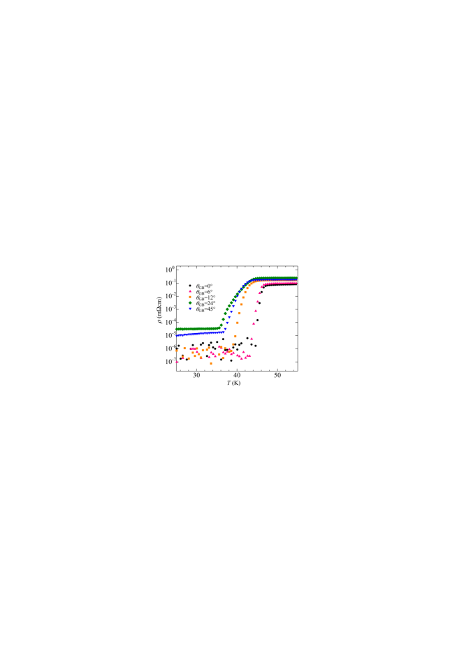
Omura have recently reported on the GB angle dependence of transport properties for NdFeAs(O,F) thin films fabricated by MBE.Omura et al. (2017) For and 12∘, the resistivity in the superconducting state was below the instrumental limitation(fig. 11). For , in contrast a finite resistivity below was observed and hence the inter-grain was zero. The inter-grain for =6∘ was reduced by nearly 30% compared to the intra-grain . Hence the critical angle for these NdFeAs(O,F) films was less than 6∘. However, the authors stated that the results did not reflect the intrinsic grain boundary properties due to the erosion of the grain boundaries by fluorine diffusion.
III.2.4 Summary of the misorientation dependence of inter-grain
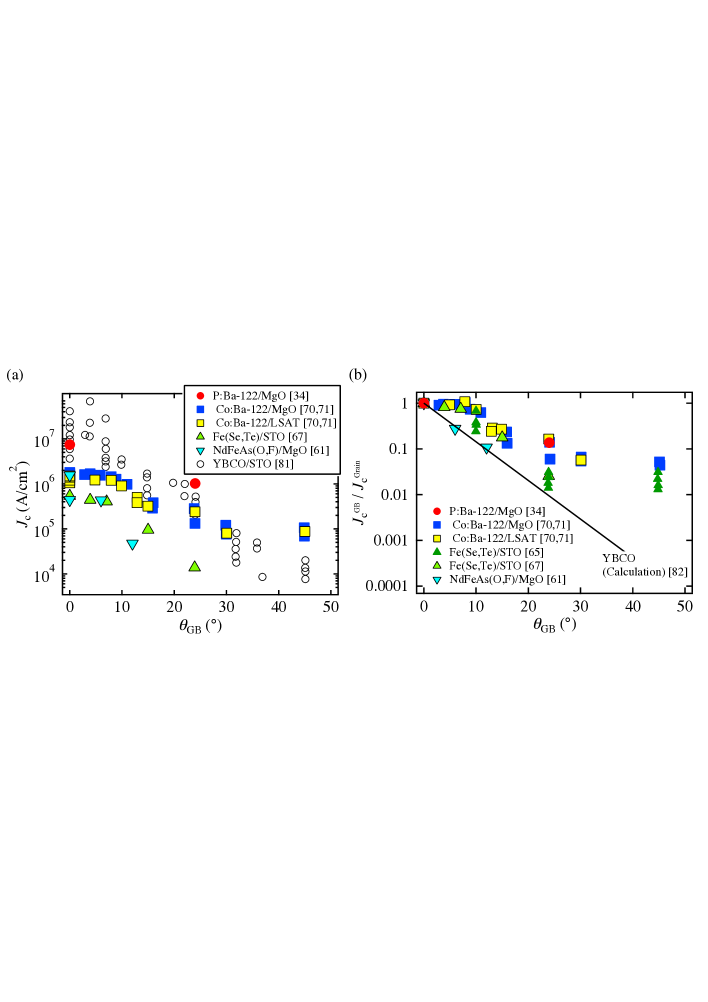
Shown in fig. 12 is a summary of dependence of inter-grain for various FBS bicrystals. Clearly, P-doped Ba-122 showed a high inter-grain of 1 MA/cm2 at (fig. 12(a)), which is highly beneficial for wire applications. It is also noted that for Ba-122 is higher than those for YBCO beyond . Although intra-grain and inter-grain are high for P-doped Ba-122, the dependence of is similar to that of Co-doped Ba-122 (fig. 12(b)). For all FBS except for NdFeAs(O,F), the critical angle is around 9∘, which indicates that in-plane misorientation alignments of FBS grains less than 9∘ usually do not impede the critical current flow. Hence one can expect that grain boundary networks whose in-plane misorientation is less than 9∘ work as flux pinning centers. Indeed, the pinning force density analysis of P-doped Ba-122 on technical substrates revealed that the GB pinning contribution is dominant for ,Sato et al. (2016); Iida et al. (2017) which will be discussed later.
The initial slope for the decrease with angle for FBS is almost similar to that of YBCO, fig. 12(b), which is different from the common belief. A distinct difference between FBS and YBCO is recognized above : for YBCO continuously decreases exponentially with , whilst remains constant for FBS. This may be due to the different symmetry: -wave for YBCO and sign reversal -wave for FBS. Additionally, the grain boundaries for both Ba-122 and Fe(Se,Te) are of metallic nature. Another plausible reason may be 45∘ [001]-tilt GBs in Ba-122 and Fe(Se,Te) compounds being special, low- or facetted GBs with a narrower structurally and electronically disturbed region than for GBs with smaller as discussed for high– cuprates.Chan (1994)
It is reported that inter-grain for YBCO is ameliorated by Ca-doping for which the depletion of the carrier density at GBs is compensated.Hammerl et al. (2000) Later, electron energy loss spectroscopy (EELS) revealed high concentrations of Ca at the tensile regions of the GBs.Song et al. (2005) On the assumption that the same mechanism could work for overdoped Ba-122, Durrell . fabricated Co-doped Ba-122 bicrystals with Co concentration from 8% (optimal) to 10% (overdoped).Durrell et al. (2011) However, no improvement of inter-grain was observed. More of such experiments should be conducted to tackle the GB problem for FBS.
IV FBS thin films on technical substrates
| Group | Materials | Substrates | Methods | performance | |||||
| BNL | Fe(Se,Te)Si et al. (2011) | IBAD-MgO | PLD |
|
|||||
| Fe(Se,Te)Si et al. (2013) |
|
PLD |
|
||||||
| IEE-CAS | Fe(Se,Te)Xu et al. (2017) |
|
PLD | 16.8 |
|
||||
| CNR | Fe(Se,Te)Braccini (2017) |
|
PLD | 18 |
|
||||
| NIMS | FeSeDemura et al. (2016) | RABiTS | EC depo. | 8 | N/A | ||||
| FeSeYamashita et al. (2018) | RABiTS | EC depo. |
|
N/A | |||||
| IFW | Co:Ba-122Iida et al. (2011b) | IBAD-MgO | PLD |
|
|||||
| Co:Ba-122Trommler et al. (2012) | IBAD-MgO | PLD |
|
||||||
| TIT | Co:Ba-122Katase et al. (2011) | IBAD-MgO | PLD |
|
|||||
| IEE-CAS | Co:Ba-122Xu et al. (2018) |
|
PLD |
|
|||||
| TIT | P:Ba-122Sato et al. (2016) | IBAD-MgO | PLD |
|
|||||
| P:Ba-122Sato et al. (2016) | IBAD-MgO | PLD |
|
||||||
| TIT | P:Ba-122Hosono et al. (2015) |
|
PLD |
|
|||||
| P:Ba-122Hosono et al. (2015) |
|
PLD |
|
||||||
| TIT | P:Ba-122Iida et al. (2017) | IBAD-MgO | PLD |
|
|||||
| Nagoya | NdFeAs(O,F)Iida et al. (2014) | IBAD-MgO | MBE | 43 |
|
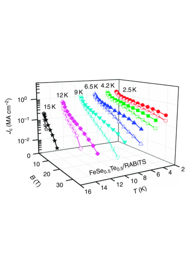
As described in the previous section, grain boundaries are less critical an issue for FBS than for cuprates, and powder-in-tube-processed wires based on 11, 122 and 1111 have been fabricated. Among them, the in-field of 122 wires has already reached the practical level of ,Huang et al. (2018) and a 120 m long tape of K-doped Sr-122 has been realized.Zhang et al. (2017a) However, biaxially textured films on single-crystalline substrates and also single crystals Ishida et al. (2017) showed superior performance to polycrystalline samples. To date, seven groups have published results on FBS films on technical substrates as prototype coated conductor samples, as summarized in Table 4. In this section, various FBS thin films on technical substrates are reviewed. Most of these studies were done on IBAD-MgO templates (textured MgO templates are prepared on Hastelloy by ion beam assisted deposition), supplied by iBeam inc., USA and Shanghai Creative Supercond. Technol. Co. Ltd, China. Three studies on FeSe and Fe(Se,Te) used RABiTS (rolling-assisted biaxially textured substrate) template for which two of them were supplied by ENEA (Italian National Agency for New Technologies, Energy and Sustainable Economic Development) and evico GmbH, Germany. The other has been fabricated by in-house R&D collaboration between Brookhaven National Laboratory and Oak Ridge National Laboratory.
IV.1 FeSe and Fe(Se,Te)
Despite the large lattice mismatch between Fe(Se,Te) ( Å) and MgO ( Å), epitaxial Fe(Se,Te) thin films were successfully fabricated on hastelloy tapes, on which epitaxial MgO templates were deposited by IBAD.Si et al. (2011) The respective in-plane and out-of-plane full width at half maximum of Fe(Se,Te) were and . Clearly, is less than the critical angle for [001]-tilt Fe(Se,Te) grain boundaries. Although a critical angle for [010]-tilt Fe(Se,Te) grain boundary junctions has not been reported, it is expected that [001]-tilt and [010]-tilt GBs in Fe(Se,Te) have a similar critical angle due to the small anisotropy and likely the sign reversal -wave type symmetry. Therefore, weak-link behavior is absent in these Fe(Se,Te) films on IBAD-MgO. The lower ( K) of that film compared to the film on LaAlO3 substrate ( K) is mostly ascribed to the large lattice misfit. The Fe(Se,Te) film showed an almost isotropic over 104 A/cm2 at 25 T and 4.2 K. The pinning force analysis revealed that point defect pinning governs the properties.
To further improve properties of Fe(Se,Te) on technical substrate, Si . have fabricated Fe(Se,Te) thin films on CeO2-buffered RABiTS.Si et al. (2013) The lattice parameter of CeO2 is around 3.82 Å(), which almost perfectly matches the in-plane lattice parameter of Fe(Se,Te). As a result, Fe(Se,Te) on RABiTS showed a high onset of over 20 K with a sharp transition of 1 K width. The structural characterization by X-ray diffraction revealed an in-plane FWHM . Despite the larger in-plane texture spread, the Fe(Se,Te) film was capable of carrying large current densities (fig. 13). A nearly isotropic MA/cm2 at 4.2 K and 30 T was observed. The pinning mechanism was the same as for the Fe(Se,Te) film on IBAD-MgO. The authors concluded that the use of CeO2 buffer layer is the key for achieving high . Additionally, the substrates containing low angle grain boundaries up to 7∘ do not impede the critical current flow, which is different from Ba2Cu3O7.
Quite recently, the group of IEE-CAS reported Fe(Se,Te) thin films on IBAD-MgO with LaMnO3 (LMO) buffer layers.Xu et al. (2017) The Fe(Se,Te) was grown on LMO with cube-on-cube configuration. The respective out-of-plane and in-plane full width at half maximum values of Fe(Se,Te) are and . The of the sample is 16.8 K, which is slightly higher than that of bulk due to the compressive strain. Albeit the large of 7.8∘, an in-field above 0.35 up to 9 T was recorded at 4.2 K. Additionally, the anisotropy of was relatively small.
The group of CNR has been recently working on an attempt to decrease the number of necessary buffer layers or exchanging the metallic substrate to less expensive materials. Both solutions could reduce the fabrication costs of such Fe(Se,Te) coated conductors.Braccini (2017) The films on Ni5W RABiTS covered with a single CeO2 buffer layer (produced by ENEA) showed a of 18 K and isotropic above A/cm2 at 4.2 K in fields up to 18 T. On biaxially textured invar (nickel-iron alloy with 36 mass% of Ni) tape, epitaxial Fe(Se,Te) layers of the same texture quality as the tape itself (FWHM 9∘) were grown without any buffer layer. The superconducting properties of these samples still have to be investigated.
The group at NIMS proposed a unique technique for fabricating FeSe films on RABiTS provided by evico GmbH.Demura et al. (2016); Yamashita et al. (2018) They performed electrochemical deposition using three electrodes, Pt (counter electrode), Ag/AgCl (reference electrode) and RABiTS (working electrode) at 70∘C. The electrolyte was prepared from a solution of FeClH2O, SeO2, and Na2SO4 in distilled water. A pH value of 2.1 for the electrode was maintained during the deposition. X-ray diffraction confirmed FeSe phase formation without heat treatment. Although the resulting film had a low of 2.5 K, this technique is promising for further development and optimization.Yamashita et al. (2018)
IV.2 Co- and P-doped Ba-122
The first report on Co-doped Ba-122 on technical substrates was published by Iida .Iida et al. (2011b) They fabricated Co-doped Ba-122 films on Fe-buffered IBAD-MgO templates by PLD. Due to the relatively large in-plane mosaicity of the MgO (), the crystalline quality of the intermediate Fe as well as Co-doped Ba-122 layers was poor (i.e., and ). Although biaxially textured Co-doped Ba-122 showed an onset of 21 K, the in-field at 8 K was almost one order of magnitude lower compared to the film on single crystalline MgO due to the poor crystalline quality. Later, employing a high-quality MgO template () improved the in-field of Co-doped Ba-122 to a level almost comparable to films on single crystalline substrates.Trommler et al. (2012)
Almost at the same time, Katase also reported on the fabrication of Co-doped Ba-122 directly on IBAD-MgO.Katase et al. (2011) A sharp texture of the Co-doped Ba-122 with was obtained irrespective of the in-plane mosaicity of MgO templates due to the self-epitaxy effect. The onset of Co-doped Ba-122 on IBAD-MgO was 22 K. In-field reached almost 0.1 MA/cm2 under 9 T at 4 K.
Very recently, Co-doped Ba-122 was also fabricated on IBAD-MgO with LMO by Xu .Xu et al. (2018) They used SrTiO3 as buffer layer between LMO and Co-doped Ba-122. The resultant film showed almost isotropic . The respective for and were 0.86 and 0.96 MA/cm2 at 9 T and 4.2 K.
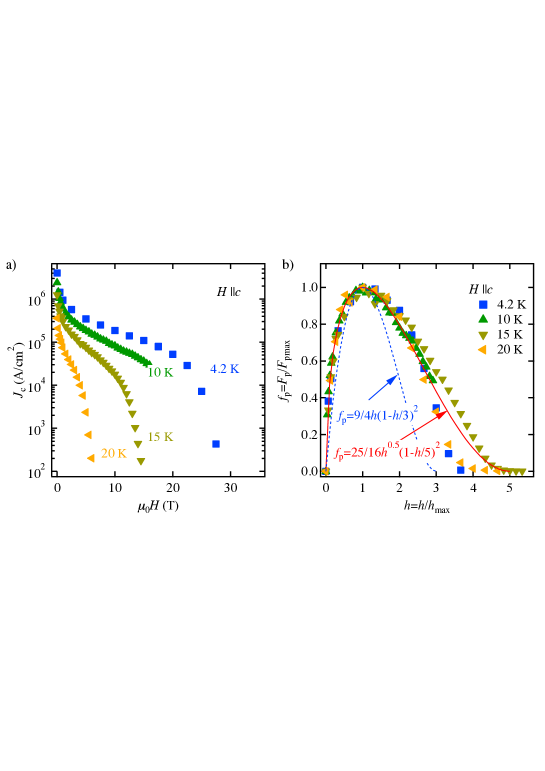
P-doped Ba-122 shows the second highest among the 122 compounds and, therefore, properties are usually superior to Co-doped Ba-122. Additionally, growth-related and artificial pinning centers can be introduced into the P-doped Ba-122 matrix as discussed in the previous section. Sato fabricated P-doped Ba-122 thin films with PLD on IBAD-MgO with two different in-plain texture qualities, and 8∘.Sato et al. (2016) The structural characterization by X-ray diffraction revealed and 8∘ for P-doped Ba-122 deposited on the well and poorly textured MgO template, respectively. The film on poor crystalline MgO template had an onset of 23 K, which is comparable to the Co-doped Ba-122 on IBAD-MgO (fig. 14(a)). On the other hand, the P-doped Ba-122 on the well textured MgO template had a higher of 26 K (fig. 14(a)). The low- sample showed nonetheless better in-field properties: almost isotropic exceeding 0.1 MA/cm2 at 9 T and 4 K (fig. 14(b)). This can be explained by grain boundary pinning. Figure 15 shows the properties of a further optimized P-doped Ba-122 thin film on IBAD-MgO ( of 28.3 K) and the corresponding normalized pinning force density () as a function of , where is the field at which the pinning force density () shows the maximum value.Iida et al. (2017) As can be seen, curves for at different temperatures almost fall onto a master curve described by
| (2) |
This formula is analogous to
| (3) |
(, and is the irreversibility field) found by Dew-Hughes for pinning by 2D defects such as grain boundaries.Dew-Hughes (1974) Recently, Paturi . found that the exponent for YBCO regardless of for a defect size in the order of coherence length.Paturi et al. (2016) On the other hand, increases to 1 with increasing defect size. This confirms that the pinning in P-doped Ba-122 on IBAD-MgO is dominated by the dislocations with nano-size.
Hosono’s group even fabricated a 10 cm long P-doped Ba-122 tape using a reel-to-reel system by PLD,Hosono et al. (2015) although the growth conditions were not fully optimized. The resultant film showed a slightly lower of 18.7 K and a low of 0.47 mA per cm-width at 4.2 K, corresponding to a of A/cm2. They also found that even short samples had a low . To improve the superconducting properties, they fabricated Fe3P/P-doped Ba-122 bilayers on IBAD-MgO. As a result, the superconducting properties were improved to K and mA per cm-width ( Acm2) at 4.2 K.
IV.3 NdFeAs(O,F)
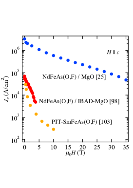
Biaxially textured NdFeAs(O,F) films on IBAD-MgO have been fabricated by MBE at Nagoya University.Iida et al. (2014) The 102 peak -scan revealed a small amount of 45∘ rotated grains. Shown in fig. 16 are properties of NdFeAs(O,F) for in comparison to data on PIT-processed SmFeAs(O,F) wires and a NdFeAs(O,F) film on single crystal MgO. Here, of NdFeAs(O,F) on IBAD-MgO was calculated from the hysteresis loops using the Bean model. The NdFeAs(O,F) thin film on IBAD template had a self-field of A/cm2 at 5 K, whereas the corresponding value for PIT-processed SmFeAs(O,F) was around A/cm2 at 4.2 K.Zhang et al. (2017b) Now the performance gap between the tape and wire is very small. However, given that of NdFeAs(O,F) on single crystalline MgO substrates is above 104 A/cm2 at 4.2 K even at fields as high as at 35 T and self-field values reach 3 MA/cm2,Tarantini et al. (2014a) there is certainly room for further improvement of superconducting properties of NdFeAs(O,F) on IBAD-MgO. The reason for the low values on IBAD templates is most likely the strong F diffusion in the GB regions, as revealed by bicrystal experiments, see above.
IV.4 Summary of FBS thin films on technical substrates
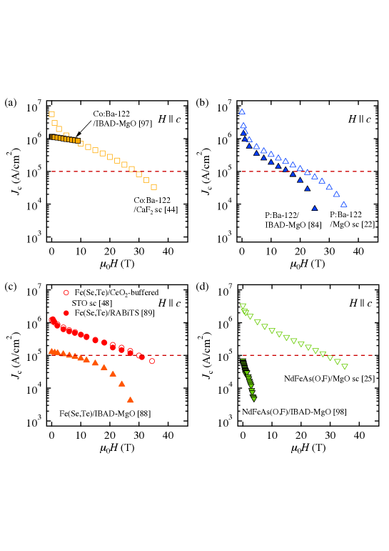
Figure 17 compares characteristics at 4.2 K of various FBS thin films on technical substrates and of high-quality FBS thin films on single-crystalline substrates. For Co-doped Ba-122, although low-field for the film on IBAD Xu et al. (2018) is lower than that for the film on single crystal,Tarantini et al. (2014b) a crossover is visible at 7.5 T. As can be seen in fig. 17(b), in-field performance for the P-doped Ba-122 on IBAD-MgOIida et al. (2017) is slightly inferior to the film on MgO single-crystalline substrateKurth et al. (2015)(fig. 17(b)). Such a difference in for the P-doped Ba-122 is mainly explained by the fact that the films on single-crystalline substrates are pinning-improved. It is expected that similar microstructures transferred to tapes would lead to similar levels. Additionally, the phase formation has to be optimized so that the full potential of the films on single crystals can be achieved on tape. On the other hand, of Fe(Se,Te) on RABiTS Si et al. (2013) is almost comparable to that of the pinning-enhanced Fe(Se,Te) thin film Ozaki et al. (2016) (fig. 17(c)). Finally, the largest discrepancy is seen for NdFeAs(O,F) on IBAD-MgO and single crystalline MgO(fig. 17(d)), which can be explained by the strong F diffusion along GBs and a concomitant broadening of their regions. This might be improved by employing flourine-free oxygen-deficient FeAsO compounds.
To evaluate the best possible performance, the ultimate critical current density, i.e., depairing current density at 4.2 K () for various FBS estimated by eqs. (4) and (5) is tabulated in table 5.
| (4) |
| (5) |
Clearly, Ba-122 compounds possess the highest among the FBS. The maximum achievable by core pinning is around 30% of the depairing current density Wimbush (2015). However, the pinning efficiency, here defined as at 4.2 K for FBS even on single crystalline substrates reaches only .
| Materials | (nm) | (nm) | (4.2 K) (MA/cm2) | (%) at 4.2 K |
|---|---|---|---|---|
| Fe(Se,Te) | 430 Klein et al. (2010) | 1.5 Klein et al. (2010) | 34 | 3.5 |
| Co-doped Ba-122 | 190 Prozorov et al. (2009) | 2.76 Prozorov et al. (2009) | 100 | 5.6 |
| P-doped Ba-122 | 200 Chaparro et al. (2012) | 2.14 Chaparro et al. (2012) | 117 | 5.4 |
| NdFeAs(O,F) | 270 Kacmarcik et al. (2009) | 2.4 Kacmarcik et al. (2009) | 57 | 5.8 |
V Summary and discussion
In order to understand the performance potential of FBS, we discussed the main application-related properties like pinning improvement by natural and artificial defects, the transparency of grain boundaries and the properties of GB networks. Naturally grown defects (BaFeO2 in Co-doped Ba-122 and threading dislocations in Fe(Se,Te)) mainly contribute to the -axis correlated pinning, and point pinning introduced by strain is beneficial as well. Artificial pinning centers can be introduced in the superconducting matrix by multilayer deposition, irradiation, and the addition of nanoparticles such as BaZrO3 to the PLD targets. Although all methods described here are effective for improving in-field properties, the level at 4.2 K achieved so far is still only up to 6% of the depairing current density in films on single crystals, suggesting room for further improvement of superconducting properties of FBS.
Bicrystal experiments on Ba-122 and Fe(Se,Te) revealed the metallic nature of grain boundaries. The critical angle above which inter-grain falls off is around 9∘. However, the initial slope for the logarithmic decrease with GB angle for FBS is similar to that of YBCO. A distinct difference between FBS and YBCO is recognised above : for YBCO continuously decreases with , whilst remains constant for FBS. Overall, those properties are highly beneficial for making cheap FBS conductors.
The three main systems with largest application potential (11, 122 and 1111) have already been realized on technical substrates. Most of the FBS coated conductor prototypes showed a comparable to their counterparts on single-crystalline substrates. Fe(Se,Te) and P-doped Ba-122 reached the practical level (0.1 MA/cm2 at 15 T). It is noted that PIT-processed FBS wires (K-doped Ba-122 and Sr-122) also have reached this level,Hosono et al. (2017) despite the presence of many GBs. Therefore, further GB experiments on FBS, especially for K-doped 122, are desired. To further improve the in-field properties of FBS on technical substrates, the introduction of artificial pinning centers without compromising is necessary .
Even though FBS tapes will never compete with YBCO tapes regarding their superconducting properties, they could compete with YBCO in terms of cost. For YBCO tapes, expensive highly-textured metallic substrates and Ag layers to allow oxygenation are necessary. However, FBS can be realized on poorly textured templates without expensive cover layers. For realizing FBS conductors, there are other properties that need to be evaluated: i) thick FBS thin films (1 m) on technical substrates should be fabricated and characterized for realizing FBS coated conductors. ii) Strain tolerance dependence of should be investigated, which is important for making a magnet.
Acknowledgements.
We thank for financial support from the EU (Iron-Sea under project number FP7-283141, SUPERIRON, Grant number 283204). This work was partially supported by the JSPS Grant-in-Aid for Scientific Research (B) Grant Number 16H04646. A portion of this work was performed at the National High Magnetic Field Laboratory, which was supported by National Science Foundation Cooperative Agreement No. DMR-1644779, and the State of Florida.References
- Kamihara et al. (2008) Y. Kamihara, T. Watanabe, M. Hirano, and H. Hosono, “Iron-Based Layered Superconductor La[O1-xFx]FeAs () with K,” J. Am. Chem. Soc. 130, 3296–3297 (2008).
- Li, Si, and Dimitrov (2011) Q. Li, W. Si, and I. K. Dimitrov, “Films of iron chalcogenide superconductors,” Rep. Prog. Phys. 74, 124510 (2011).
- Hiramatsu et al. (2012a) H. Hiramatsu, T. Katase, T. Kamiya, and H. Hosono, “Thin Film Growth and Device Fabrication of Iron-Based Superconductors,” J. Phys. Soc. Jpn. 81, 011011 (2012a).
- Mele (2012) P. Mele, “Superconducting properties of iron chalcogenide thin films,” Sci. Technol. Adv. Mater. 13, 054301 (2012).
- Haindl et al. (2014) S. Haindl, M. Kidszun, S. Oswald, C. Hess, B. Büchner, S. Kölling, L. Wilde, T. Thersleff, V. V. Yurchenko, M. Jourdan, H. Hiramatsu, and H. Hosono, “Thin film growth of Fe-based superconductors: from fundamental properties to functional devices. A comparative review,” Rep. Prog. Phys. 77, 046502 (2014).
- Imai, Nabeshima, and Maeda (2017) Y. Imai, F. Nabeshima, and A. Maeda, “Comparative Review on Thin Film Growth of Iron-Based Superconductors,” Condens. Matter 2, 25 (2017).
- Hosono et al. (2015) H. Hosono, K. Tanabe, E. Takayama-Muromachi, H. Kageyama, S. Yamanaka, H. Kumakura, M. Nohara, H. Hiramatsu, and S. Fujitsu, “Exploration of new superconductors and functional materials, and fabrication of superconducting tapes and wires of iron pnictides,” Sci. Technol. Adv. Mater. 16, 033503 (2015).
- Hosono et al. (2017) H. Hosono, A. Yamamoto, H. Hiramatsu, and Y. Ma, “Recent advances in iron-based superconductors towards applications,” Mater. Today 21, 278–302 (2017).
- Sakoda, Iida, and Naito (2018) M. Sakoda, K. Iida, and M. Naito, “Recent progress in thin-film growth of Fe-based superconductors: superior superconductivity achieved by thin films,” Supercond. Sci. Technol. (2018), DOI:10.1088/1361-6668/aabddb.
- Yang et al. (2017) H. Yang, G. Chen, X. Zhu, J. Xing, and H.-H. Wen, “BCS-like critical fluctuations with limited overlap of Cooper pairs in FeSe,” Phys. Rev. B 96, 064501 (2017).
- Klein et al. (2010) T. Klein, D. Braithwaite, A. Demuer, A. Knafo, G. Lapertot, C. Marcenat, P. Rodière, I. Sheikin, P. Strobel, P. Sulpice, and P. Toulemonde, “Thermodynamic phase diagram of Fe(Se0.5Te0.5) single crystals in fields up to 28 tesla,” Phys. Rev. B 82, 184506 (2010).
- Yamamoto et al. (2009) A. Yamamoto, J. Jaroszynski, C. Tarantini, L. Balicas, J. Jiang, A. Gurevich, D. C. Larbalestier, R. Jin, A. S. Sefat, M. A. McGuire, B. C. Sales, D. K. Christen, and D. Mandrus, “Small anisotropy, weak thermal fluctuations, and high field superconductivity in Co-doped iron pnictide Ba(Fe1-xCox)2As2,” Appl. Phys. Lett. 94, 062511 (2009).
- Chaparro et al. (2012) C. Chaparro, L. Fang, H. Claus, A. Rydh, G. W. Crabtree, V. Stanev, W. K. Kwok, and U. Welp, “Doping dependence of the specific heat of single-crystal BaFe2(As1-xPx)2,” Phys. Rev. B 85, 184525 (2012).
- Kacmarcik et al. (2009) J. Kacmarcik, C. Marcenat, T. Klein, Z. Pribulova, C. J. van der Beek, M. Konczykowski, S. K. Bud’ko, M. Tillman, N. Ni, and P. C. Canfield, “Strongly dissimilar vortex-liquid regimes in single-crystalline NdFeAs(O,F) and (Ba,K)Fe2As2: A comparative study,” Phys. Rev. B 80, 014515 (2009).
- Jaroszynski et al. (2008) J. Jaroszynski, S. C. Riggs, F. Hunte, D. C. L. A. Gurevich, G. S. Boebinger, F. F. Balakirev, A. Migliori, Z. A. Ren, W. Lu, J. Yang, X. L. Shen, X. L. Dong, Z. X. Zhao, R. Jin, A. S. Sefat, M. A. McGuire, B. C. Sales, D. K. Christen, and D. Mandrus, “Comparative high-field magnetotransport of the oxypnictide superconductors FeAsO1-xFx (=La, Nd) and SmFeAsO1-δ,” Phys. Rev. B 78, 064511 (2008).
- Zehetmayer et al. (2002) M. Zehetmayer, M. Eisterer, J. Jun, S. M. Kazakov, J. Karpinski, A. Wisniewski, and H. W. Weber, “Mixed-state properties of superconducting MgB2 single crystal,” Phys. Rev. B 66, 052505 (2002).
- Putti et al. (2010) M. Putti, I. Pallecchi, E. Bellingeri, M. R. Cimberle, M. Tropeano, C. Ferdeghini, A. Palenzona, C. Tarantini, A. Yamamoto, J. Jiang, J. Jaroszynski, F. Kametani, D. Abraimov, A. Polyanskii, J. D. Weiss, E. E. Hellstrom, A. Gurevich, D. C. Larbalestier, R. Jin, B. C. Sales, A. S. Sefat, M. A. McGuire, D. Mandrus, P. Cheng, Y. Jia, H. H. Wen, S. Lee, and C. B. Eom, “New Fe-based superconductors: properties relevant for applications,” Supercond. Sci. Technol. 23, 034003 (2010).
- Blatter et al. (1994) G. Blatter, M. V. Feigel’man, V. B. Geshkenbein, A. I. Larkin, and V. M. Vinokur, “Vortices in high-temperature superconductors,” Rev. Mod. Phys. 66, 1125–1388 (1994).
- Eley et al. (2017) S. Eley, M. Miura, B. Maiorov, and L. Civale, “Universal lower limit on vortex creep in superconductors,” Na. Mater. 16, 409–413 (2017).
- Lee et al. (2010) S. Lee, J. Jiang, Y. Zhang, C. W. Bark, J. D. Weiss, C. Tarantini, C. T. Nelson, H. W. Jang, C. M. Folkman, S. H. Baek, A. Polyanskii, D. Abraimov, A. Yamamoto, J. W. Park, X. Q. Pan, E. E. Hellstrom, D. C. Larbalestier, and C. B. Eom, “Template engineering of Co-doped BaFe2As2 single-crystal thin films,” Nat. Mater. 9, 397–402 (2010).
- Ishida et al. (2017) S. Ishida, D. Song, H. Ogino, A. Iyo, H. Eisaki, M. Nakajima, J. Shimoyama, and M. Eisterer, “Doping-dependent critical current properties in K, Co, and P-doped BaFe2As2 single crystals,” Phys. Rev. B 95, 014517 (2017).
- Kurth et al. (2015) F. Kurth, C. Tarantini, V. Grinenko, J. Hänisch, J. Jaroszynski, E. Reich, Y. Mori, A. Sakagami, T. Kawaguchi, J. Engelmann, L. Schultz, B. Holzapfel, H. Ikuta, R. Hühne, and K. Iida, “Unusually high critical current of clean P-doped BaFe2As2 single crystalline thin film,” Appl. Phys. Lett. 106, 072602 (2015).
- Iida et al. (2011a) K. Iida, J. Hänisch, M. Schulze, S. Aswartham, S. Wurmehl, B. Büchner, L. Schultz, and B. Holzapfel, “Generic Fe buffer layers for Fe-based superconductors: Epitaxial FeSe1-xTex thin films,” Appl. Phys. Lett. 99, 202503 (2011a).
- Sun et al. (2013) Y. Sun, T. Taen, Y. Tsuchiya, Q. Ding, S. Pyon, Z. Shi, and T. Tamegai, “Large, Homogeneous, and Isotropic Critical Current Density in Oxygen-Annealed Fe1+yTe0.6Se0.4 Single Crystal,” Appl. Phys. Express 6, 043101 (2013).
- Tarantini et al. (2014a) C. Tarantini, K. Iida, J. Hänisch, F. Kurth, J. Jaroszynski, N. Sumiya, M. Chihara, T. Hatano, H. Ikuta, S. Schmidt, P. Seidel, B. Holzapfel, and D. C. Larbalestier, “Intrinsic and extrinsic pinning in NdFeAs(O,F): vortex trapping and lock-in by the layered structure,” Sci. Rep. 6, 36047 (2014a).
- Eisterer et al. (2014) M. Eisterer, V. Mishev, M. Zehetmayer, N. D. Zhigadlo, S. Katrych, and J. Karpinski, “Critical current anisotropy in Nd-1111 single crystals and the influence of neutron irradiation,” Supercond. Sci. Technol. 27, 044009 (2014).
- Matsumoto and Mele (2010) K. Matsumoto and P. Mele, “Artificial pinning center technology to enhance vortex pinning in YBCO coated conductors,” Supercond. Sci. Technol. 23, 014001 (2010).
- Tarantini et al. (2010a) C. Tarantini, S. Lee, Y. Zhang, J. Jiang, C. W. Bark, J. D. Weiss, A. Polyanskii, C. T. Nelson, H. W. Jang, C. M. Folkman, S. H. Baek, X. Q. Pan, A. Gurevich, E. E. Hellstrom, C. B. Eom, and D. C. Larbalestier, “Strong vortex pinning in Co-doped BaFe2As2 single crystal thin films,” Appl. Phys. Lett. 96, 142510 (2010a).
- Tarantini et al. (2012) C. Tarantini, S. Lee, F. Kametani, J. J. andJ. D. Weiss, J. Jaroszynski, C. M. Folkman, E. E. Hellstrom, C. B. Eom, and D. C. Larbalestier, “Artificial and self-assembled vortex-pinning centers in superconducting Ba(Fe1-xCox)2As2 thin films as a route to obtaining very high critical-current densities,” Phys. Rev. B 86, 214504 (2012).
- Zhang et al. (2011) Y. Zhang, C. T. Nelson, S. Lee, J. Jiang, C. W. Bark, J. D. Weiss, C. Tarantini, C. M. Folkman, S. H. Baek, E. E. Hellstrom, D. C. Larbalestier, C. B. Eom, and P. X, “Self-assembled oxide nanopillars in epitaxial BaFe2As2 thin films for vortex pinning,” Appl. Phys. Lett. 98, 042509 (2011).
- Bellingeri et al. (2012) E. Bellingeri, S. Kawale, I. Pallecchi, A. Gerbi, R. Buzio, V. Braccini, A. Palenzona, M. Putti, M. Adamo, E. Sarnelli, and C. Ferdeghini, “Strong vortex pinning in FeSe0.5Te0.5 epitaxial thin film,” Appl. Phys. Lett. 100, 082601 (2012).
- Sato et al. (2014) H. Sato, H. Hiramatsu, T. Kamiya, and H. Hosono, “High critical-current density with less anisotropy in BaFe2(As,P)2 epitaxial thin films: Effect of intentionally grown -axis vortex-pinning centers,” Appl. Phys. Lett. 104, 182603 (2014).
- Hänisch et al. (2014) J. Hänisch, K. Iida, F. Kurth, T. Thersleff, S. Trommler, E. Reich, R. Hühne, L. Schultz, and B. Holzapfel, “The effect of 45∘ grain boundaries and associated Fe particles on and resistivity in Ba(Fe0.9Co0.1)2As2 thin films,” AIP Conference Proceedings 1574, 260 (2014).
- Sakagami et al. (2013) A. Sakagami, T. Kawaguchi, M. Tabuchi, T. Ujihara, Y. Takeda, and H. Ikuta, “Critical current density and grain boundary property of BaFe2(As,P)2 thin films,” Physica C 494, 181–184 (2013).
- MacManus-Driscoll et al. (2004) J. L. MacManus-Driscoll, S. R. Foltyn, Q. X. Jia, H. Wang, A. Serquis, L. Civale, B. Maiorov, M. E. Hawley, M. P. Maley, and D. E. Peterson, “Strongly enhanced current densities in superconducting coated conductors of YBa2Cu3O7-x + BaZrO3,” Nat. Mater. 3, 439–443 (2004).
- Miura et al. (2013) M. Miura, B. Maiorov, T. Kato, T. Shimode, K. Wada, S. Adachi, and K. Tanabe, “Strongly enhanced flux pinning in one-step deposition of BaFe2(As0.66P0.33)2 superconductor films with uniformly dispersed BaZrO3 nanoparticles,” Nat. Commun. 4, 2499 (2013).
- Lee et al. (2017) J. Lee, J. Jiang, F. Kametani, M. J. Oh, J. D. Weiss, Y. Collantes, S. Seo, S. Yoon, C. Tarantini, Y. J. Jo, E. E. Hellstrom, and S. Lee, “High critical current density over 1 MAcm-2 at 13 T in BaZrO3 incorporated Ba(Fe,Co)2As2 thin film,” Supercond. Sci. Technol. 30, 085006 (2017).
- Chepikov et al. (2017) V. Chepikov, N. Mineev, P. Degtyarenko, S. Lee, V. Petrykin, A. Ovcharov, A. Vasiliev, A. Kaul, V. Amelichev, A. Kamenev, A. Molodyk, and S. Samoilenkov, “Introduction of BaSnO3 and BaZrO3 artificial pinning centres into 2G HTS wires based on PLD-GdBCO films. Phase I of the industrial R&D programme at SuperOx,” Supercond. Sci. Technol. 30, 124001 (2017).
- Birlik et al. (2010) I. Birlik, M. Erbe, T. Freudenberg, E. Celik, L. Schultz, and B. Holzapfel, “Flux pinning improvement of ybco superconducting films with BaZrO3 nanoparticles prepared by chemical solution deposition method,” J. Phys. : Conf. Ser. 234, 012004 (2010).
- Horide et al. (2017) T. Horide, F. Kametani, S. Yoshioka, T. Kitamura, and K. Matsumoto, “Structural Evolution Induced by Interfacial Lattice Mismatch in Self-Organized YBa2Cu3O7-δ Nanocomposite Film,” ACS Nano 11, 1780–1788 (2017).
- Goyal et al. (2005) A. Goyal, S. Kang, K. J. Leonard, P. M. Martin, A. A. Gapud, M. Varela, M. Paranthaman, A. O. Ijaduola, E. D. Specht, J. R. Thompson, D. K. Christen, S. J. Pennycook, and F. A. List, “Irradiation-free, columnar defects comprised of self-assembled nanodots and nanorods resulting in strongly enhanced flux-pinning in YBa2Cu3O7-δ films,” Supercond. Sci. Technol. 18, 1533 (2005).
- Lee et al. (2013) S. Lee, C. Tarantini, P. Gao, J. Jiang, J. D. Weiss, F. Kametani, C. M. Folkman, Y. Zhang, X. Q. Pan, E. E. Hellstrom, D. C. Larbalestier, and C. B. Eom, “Artificially engineered superlattices of pnictide superconductors,” Nat. Mater. 12, 392–396 (2013).
- Nabeshima et al. (2017) F. Nabeshima, Y. Imai, A. Ichinose, I. Tsukada, and A. Maeda, “Growth and transport properties of FeSe/FeTe superlattice thin films,” Jpn. J. Appl. Phys. 56, 020308 (2017).
- Tarantini et al. (2014b) C. Tarantini, F. Kametani, S. Lee, J. Jiang, J. D. Weiss, J. Jaroszynski, E. E. Hellstrom, C. B. Eom, and D. C. Larbalestier, “Development of very high in Ba(Fe1-xCox)2As2 thin films grown on CaF2,” Sci. Rep. 4, 7305 (2014b).
- Engelmann et al. (2013) J. Engelmann, K. Iida, F. Kurth, C. Behler, S. Oswald, R. Hühne, B. Holzapfel, L. Schultz, and D. Haindl, “Fe/Ba(Fe1-xCox)2As2 multilayers and quasi-multilayers with =29 K,” Physica C 494, 185–188 (2013).
- Chen et al. (2012) L. Chen, C. F. Tsai, Y. Zhu, A. Chen, Z. Bi, J. Lee, and H. Wang, “Enhanced flux pinning properties in superconducting FeSe0.5Te0.5 thin films with secondary phases,” Supercond. Sci. Technol. 25, 025020 (2012).
- Eisterer et al. (2011) M. Eisterer, R. Raunicher, H. W. Weber, E. Bellingeri, M. R. Cimberle, I. Pallecchi, M. Putti, and C. Ferdeghini, “Anisotropic critical currents in FeSe0.5Te0.5 films and the influence of neutron irradiation,” Supercond. Sci. Technol. 24, 065016 (2011).
- Ozaki et al. (2016) T. Ozaki, L. Wu, C. Zhang, J. Jaroszynski, W. Si, J. Zhou, Y. Zhu, and Q. Li, “A route for a strong increase of critical current in nanostrained iron-based superconductors,” Nat. Commun. 7, 13036 (2016).
- Ozaki et al. (2018) T. Ozaki, L. Wu, C. Zhang, W. Si, Q. Jie, and Q. Li, “Enhanced critical current in superconducting FeSe0.5Te0.5 films at all magnetic field orientations by scalable gold ion irradiation,” Supercond. Sci. Technol. 31, 024002 (2018).
- Ahmad et al. (2017) D. Ahmad, W. J. Choi, Y. I. Seo, S. Seo, S. Lee, T. Park, J. Mosqueira, G. Gu, and Y. S. Kwon, “Effect or proton irradiation on the fluctuation-induced magnetoconductivity of FeSe1-xTex thin films,” New J. Phys. 19, 093004 (2017).
- Sylva et al. (2018) G. Sylva, E. Bellingeri, C. Ferdeghini, A. Martinelli, I. Pallecchi, L. Pellegrino, M. Putti, G. Ghigo, L. Gozzelino, D. Torsello, G. Grimaldi, A. Leo, A. Nigro, and V. Braccini, “Effects of high energy proton irradiation on the superconducting properties of Fe(Se,Te) thin films,” Supercond. Sci. Technol. (2018), https://doi.org/10.1088/1361-6668/aab3bd.
- Janaki et al. (2014) J. Janaki, T. Kumar, A. Mani, E. P. Amaladass, N. Raveendran, P. Magudapathy, S. Kalavathi, T. N. Sairam, and T. R. Ravindran, “Characterization and Low Temperature Study of Iron Telluride Thin Films Upon Ageing and Oxygen Ion Irradiation,” J. Supercond. Nov. Magn. 27, 2639–2643 (2014).
- Maiorov et al. (2012) B. Maiorov, T. Katase, O. Usov, M. Weigand, L. Civale, H. Hiramatsu, and H. Hosono, “Competition and cooperation of pinning by extrinsic point-like defects and intrinsic strong columnar defects in BaFe2As2 thin films,” Phys. Rev. B 86, 094513 (2012).
- Schilling et al. (2016) M. B. Schilling, A. Baumgartner, B. Gorshunov, E. S. Zhukova, V. A. Dravin, K. V. Misten, D. V. Efremov, O. V. Dolgov, K. Iida, M. Dressel, and S. Zapf, “Tracing the symmetry in iron pnictides by controlled disorder,” Phys. Rev. B 93, 174515 (2016).
- Daghero et al. (2017) D. Daghero, M. Tortello, L. Gozzelino, R. S. Gonnelli, T. Hatano, T. Kawaguchi, and H. Ikuta, “Effect of ion irradiation on surface morphology and superconductivity of BaFe2(As1-xPx)2 films,” Appl. Surf. Sci. 395, 9–15 (2017).
- Tarantini et al. (2018) C. Tarantini, K. Iida, N. Sumiya, C. Chihara, T. Hatano, H. Ikuta, R. K. Singh, N. Newman, and D. C. Larbalestier, “Effect of -particle irradiation on a NdFeAs(O,F) thin film,” Supercond. Sci. Technol. 31, 034002 (2018).
- Eisterer (2018) M. Eisterer, “Radiation effects on iron-based superconductors,” Supercond. Sci. Technol. 31, 013001 (2018).
- Efremov et al. (2011) D. V. Efremov, M. M. Korshunov, O. V. Dolgov, A. A. Golubov, and P. J. Hirschfeld, “Disorder-induced transition between and states in two-band superconductors,” Phys. Rev. B 84, 180512 (2011).
- Tarantini et al. (2010b) C. Tarantini, M. Putti, A. Gurevich, Z. Shen, R. K. Singh, J. M. Rowell, N. Newman, D. C. Larbalestier, P. Cheng, Z. Jia, and H.-H. Wen, “Suppression of the Critical Temperature of Superconducting NdFeAs(O,F) Single Crystals by Kondo-Like Defects Sites Induced by -Particle Irradiation,” Phys. Rev. Lett. 104, 087002 (2010b).
- Held et al. (2009) R. Held, C. W. Schneider, J. Mannhart, L. F. Allard, K. L. More, and A. Goyal, “Low-angle grain boundaries in YBa2Cu3O7-δ with high critical current densities,” Phys. Rev. B 79, 014515 (2009).
- Omura et al. (2017) T. Omura, T. Matsumoto, T. Hatano, K. Iida, and H. Ikuta, “Fabrication of grain boundary junctions using NdFeAs(O,F) superconducting thin films,” (2017), arXiv:1712.05966 .
- Deutscher (2010) G. Deutscher, “Origin of weak-link behavior of grain boundaries in superconducting cuprates and pnictides,” Appl. Phys. Lett. 96, 122502 (2010).
- Durrell et al. (2011) J. H. Durrell, C.-B. Eom, A. Gurevich, E. E. Hellstrom, C. Tarantini, A. Yamamoto, and D. C. Larbalestier, “The behavior of grain boundaries in the Fe-based superconductors,” Rep. Prog. Phys. 74, 124511 (2011).
- Sarnelli et al. (2014) E. Sarnelli, M. Adamo, C. Nappi, V. Braccini, S. Kawale, E. Bellingeri, and C. Ferdeghini, “Properties of high-angle Fe(Se,Te) bicrystal grain boundary junctions,” Appl. Phys. Lett. 104, 162601 (2014).
- Sarnelli et al. (2017a) E. Sarnelli, C. Nappi, C. Camerlingo, E. Enrico, E. Bellingeri, S. Kawale, V. Braccini, A. Leveratto, and C. Ferdeghini, “Properties of Fe(Se,Te) Bicrystal Grain Boundary Junctions, SQUIDs, and Nanostrips,” IEEE Trans. Appl. Supercond. 27, 7400104 (2017a).
- Sarnelli et al. (2017b) E. Sarnelli, C. Nappi, A. Leveratto, E. Bellingeri, V. Braccini, and C. Ferdeghini, “Fe(Se,Te) superconducting quantum interference devices,” Supercond. Sci. Technol. 30, 065003 (2017b).
- Si et al. (2015) W. Si, C. Zhang, X. Shi, T. Ozaki, J. Jaroszynski, and Q. Li, “Grain boundary junctions of FeSe0.5Te0.5 thin films on SrTiO3 bi-crystal substrates,” Appl. Phys. Lett. 106, 032602 (2015).
- Lee et al. (2009) S. Lee, J. Jiang, J. D. Weiss, C. M. Folkman, C. W. Bark, C. Tarantini, A. Xu, D. Abraimov, A. Polyanskii, C. T. Nelson, Y. Zhang, S. H. Baek, H. W. Jang, A. Yamamoto, F. Kametani, X. Q. Pan, E. E. Hellstrom, A. Gurevich, C. B. Eom, and D. C. Larbalestier, “Weak-link behavior of grain boundaries in superconducting Ba(Fe0.5Cox)2As2 bicrystals,” Appl. Phys. Lett. 95, 212505 (2009).
- Schmidt et al. (2013) S. Schmidt, S. Döring, F. Schmidl, V. Tympel, S. Haindl, K. Iida, F. Kurth, B. Holzapfel, and P. Seidel, “Bicrystalline Grain Boundary and Hybrid SNS Junctions Based on Ba-122 Thin Films,” IEEE Trans. Appl. Supercond. 23, 7300104 (2013).
- Katase et al. (2013) T. Katase, Y. Ishimaru, A. Tsukamoto, H. Hiramatsu, T. Kamiya, K. Tanabe, and H. Hosono, “Advantageous grain boundaries in iron pnictide superconductors,” Nat. Commun. 2, 409 (2013).
- Hiramatsu et al. (2012b) H. Hiramatsu, T. Katase, Y. Ishimaru, A. Tsukamoto, T. Kamiya, K. Tanabe, and H. Hoson, “Microstructure and transport properties of [001]-tilt bicrystal grain boundaries in iron pnictide superconductor, cobalt-doped BaFe2As2,” Mater. Sci. Eng., B 177, 515–519 (2012b).
- Iida et al. (2012) K. Iida, S. Haindl, F. Kurth, J. Hänisch, L. Schultz, and B. Holzapfel, “BaFe2As2/Fe bilayers with [001]-tilt grain boundary on MgO and SrTiO3 bicrystal substrates,” Physics Procedia 45, 189–192 (2012).
- Katase et al. (2010a) T. Katase, Y. Ishimaru, A. Tsukamoto, H. Hiramatsu, T. Kamiya, K. Tanabe, and H. Hosono, “Josephson junction in cobalt-doped BaFe2As2 epitaxial thin films on (La,Sr)(Al,Ta)O3 bicrystal substrates,” Appl. Phys. Lett. 96, 142507 (2010a).
- Katase et al. (2010b) T. Katase, Y. Ishimaru, A. Tsukamoto, H. Hiramatsu, T. Kamiya, K. Tanabe, and H. Hosono, “DC superconducting quantum interference devices fabricated using bicrystal grain boundary junctions in Co-doped BaFe2As2 epitaxial films,” Supercond. Sci. Technol. 23, 082001 (2010b).
- Schmidt et al. (2014) S. Schmidt, S. Döring, F. Schmidl, F. Kurth, K. Iida, B. Holzapfel, T. Kawaguchi, Y. Mori, H. Ikuta, and P. Seidel, “Bicrystalline Grain Boundary Junctions of Co-doped and P-doped Ba-122 Thin Films,” J. Phys.: Conf. Ser. 507, 012046 (2014).
- Seidel (2011) P. Seidel, “Josephson effects in iron based superconductors,” Supercond. Sci. Technol. 24, 043001 (2011).
- Kim et al. (2014) Y.-J. Kim, J. D. Weiss, E. E. Hellstrom, D. C. Larbalestier, and D. N. Seidman, “Evidence for composition variations and impurity segregation at grain boundaries in high current-density polycrystalline K- and Co-doped BaFe2As2 superconductors,” Appl. Phys. Lett. 105, 162604 (2014).
- Weiss et al. (2012) J. D. Weiss, C. Tarantini, J. Jiang, F. Kametani, A. A. Polyanskii, D. C. Larbalestier, and E. E. Hellstrom, “High intergrain critical current density in fine-grain (Ba0.6K0.4)Fe2As2 wires and bulks,” Nat. Mater. 11, 682–685 (2012).
- Weiss et al. (2015) J. D. Weiss, A. Yamamoto, A. A. Polyanskii, R. B. Richardson, D. C. Larbalestier, and E. E. Hellstrom, “Demonstration of an iron-pnictide bulk superconducting magnet capable of trapping over 1 T,” Supercond. Sci. Technol. 28, 112001 (2015).
- Zhang et al. (2015) Q. Zhang, H. Lin, P. Yuan, X. Zhang, C. Yao, D. Wang, C. Dong, Y. Ma, S. Awaji, and K. Watanabe, “Low-temperature synthesis to achieve high critical current density and avoid a reaction layer in SmFeAsO1-xFx superconducting tapes,” Supercond. Sci. Technol. 28, 6105005 (2015).
- Hilgenkamp and Mannhart (2002) H. Hilgenkamp and J. Mannhart, “Grain boundaries in high– superconductors,” Rev. Mod. Phys. 74, 485–549 (2002).
- Graser et al. (2010) S. Graser, P. J. Hirschfeld, T. Kopp, R. Gutser, B. M. Andersen, and J. Mannhart, “How grain boundaries limit supercurrents in high-temperature superconductors,” Nat. Phys. 6, 609–614 (2010).
- Sato et al. (2016) H. Sato, H. Hiramatsu, T. Kamiya, and H. Hosono, “Enhanced critical-current in P-doped BaFe2As2 thin films on metal substrates arising from poorly aligned grain boundaries,” Sci. Rep. 6, 36828 (2016).
- Iida et al. (2017) K. Iida, H. Sato, C. Tarantini, J. Hänisch, J. Jaroszynski, H. Hiramatsu, B. Holzapfel, and H. Hosono, “High-field transport properties of a P-doped BaFe2As2 film on technical substrate,” Sci. Rep. 7, 39951 (2017).
- Chan (1994) S.-W. Chan, “Nature of grain boundaries as related to critical currents in superconducting YBa2Cu3O7-x,” J. Phys. Chem. Solids 55, 1415–1432 (1994).
- Hammerl et al. (2000) G. Hammerl, A. Schmehl, R. R. Schultz, B. Götz, H. Bielefeldt, C. W. Schneider, H. Hilgenkamp, and J. Mannhart, “Enhanced supercurrent density in polycrystalline YBa2Cu3O7-δ at 77 K from calcium doping grain boundaries,” Nature 407, 162–164 (2000).
- Song et al. (2005) X. Song, G. Daniels, D. M. Feldmann, A. Gurevich, and D. C. Larbalestier, “Electromagnetic, atomic structure and chemistry changes induced by Ca-doping of low-angle YBa2Cu3O7-δ grain boundaries,” Nat. Mater. 4, 470–475 (2005).
- Si et al. (2011) W. Si, J. Zhou, Q. Jie, I. Dimitrov, V. Solovyov, P. D. Johnston, J. Jaroszynski, V. Matias, C. Sheehan, and Q. Li, “Iron-chalcogenide FeSe0.5Te0.5 coated superconducting tapes for high field applications,” Appl. Phys. Lett. 98, 262509 (2011).
- Si et al. (2013) W. Si, S. J. Han, X. Shi, S. N. Ehrlich, J. Jaroszynski, A. Goyal, and Q. Li, “High current superconductivity in FeSe0.5Te0.5-coated conductors at 30 tesla,” Nat. Commun. 4, 1347 (2013).
- Xu et al. (2017) Z. Xu, P. Yuan, Y. Ma, and C. Cai, “High-performance FeSe0.5Te0.5 thin films fabricated on less-well-textured flexible coated conductor templates,” Supercond. Sci. Technol. 30, 035003 (2017).
- Braccini (2017) V. Braccini, “Fe(Se,Te) epitaxial thin films deposited on flexible metallic substrates,” (2017), 13 th biennial European Conference on Applied Superconductivity, EUCAS 2017, Geneva, Switzerland.
- Demura et al. (2016) S. Demura, M. Tanaka, A. Yamashita, S. J. Denholme, H. Okazaki, M. Fujioka, T. Yamaguchi, H. Takeya, K. Iida, B. Holzapfel, H. Sakata, and Y. Takano, “Electrochemical Deposition of FeSe on RABiTS Tapes,” J. Phys. Soc. Jpn. 85, 015001 (2016).
- Yamashita et al. (2018) A. Yamashita, R. Matsumoto, M. Tanaka, H. Hara, K. Iida, B. Holzapfel, H. Takeya, and Y. Takano, “Observation of zero resistance in as-electrodeposited FeSe,” Solid State Commun. 270, 72–75 (2018).
- Iida et al. (2011b) K. Iida, J. Hänisch, S. Trommler, V. Matias, S. Haindl, F. Kurth, I. L. del Pozo, R. Hühne, M. Kidszun, J. Engelmann, L. Schultz, and B. Holzapfel, “Epitaxial Growth of Superconducting Ba(Fe1-xCox)2As2 Thin Films on Technical Ion Beam Assisted Deposition MgO Substrates,” Appl. Phys. Express 4, 013103 (2011b).
- Trommler et al. (2012) S. Trommler, J. Hänisch, V. Matias, R. Hühne, E. Reich, K. Iida, S. Haindl, L. Shultz, and B. Holzapfel, “Architecture, microstructure and anisotropy of highly oriented biaxially textured Co-doped BaFe2As2 on Fe/IBAD-MgO-buffered metal tapes,” Supercond. Sci. Technol. 25, 084019 (2012).
- Katase et al. (2011) T. Katase, H. Hiramatsu, V. Matias, C. Sheehan, Y. Ishimaru, T. Kamiya, K. Tanabe, and H. Hosono, “Biaxially textured cobal-doped BaFe2As2 films with high critical current density over 1 MA/cm2 on MgO-buffered metal-tape flexible substrates,” Appl. Phys. Lett. 98, 242510 (2011).
- Xu et al. (2018) Z. Xu, P. Yuan, F. Fan, Y. Chen, and Y. Ma, “Transport properties and pinning analysis for Co-doped BaFe2As2 thin films on metal tapes,” Supercond. Sci. Technol. 31, 055001 (2018).
- Iida et al. (2014) K. Iida, F. Kurth, M. Chihara, N. Sumiya, V. Grinenko, A. Ichinose, I. Tsukada, J. Hänisch, V. Matias, T. Hatano, B. Holzapfel, and H. Ikuta, “Highly textured oxypnictide superconducting films on metal substrates,” Appl. Phys. Lett. 105, 172602 (2014).
- Huang et al. (2018) H. Huang, C. Yao, C. Dong, X. Zhang, D. Wang, Z. Cheng, J. Li, S. Awaji, H. Wen, and Y. Ma, “High transport current superconductivity in powder-in-tube Ba0.6K0.4Fe2As2 tapes at 27 T,” Supercond. Sci. Technol. 31, 015017 (2018).
- Zhang et al. (2017a) X. Zhang, H. Oguro, C. Yao, C. Dong, Z. Xu, D. Wang, S. Awaji, K. Watanabe, and Y. Ma, “Superconducting Properties of 100-m Class Sr0.6K0.4Fe2As2 Tape and Pancake Coils superconducting tapes,” IEEE Trans. Appl. Supercond. 27, 7300705 (2017a).
- Dew-Hughes (1974) D. Dew-Hughes, “Flux pinning mechanism in type II superconductors,” Philos. Mag. 30, 293–305 (1974).
- Paturi et al. (2016) P. Paturi, M. Malmivirta, H. Palonen, and H. Huhtinen, “Dopant Diameter Dependence of in Doped YBCO Films,” IEEE Trans. Appl. Supercond. 26, 8000705 (2016).
- Zhang et al. (2017b) Q. Zhang, X. Zhang, C. Yao, H. Huang, D. Wang, C. Dong, Y. Ma, H. Ogino, and S. Awaji, “Enhanced transport current density in Sn-doped SmFeAsO1-xFx tapes prepared by the PIT method,” Supercond. Sci. Technol. 30, 065004 (2017b).
- Wimbush (2015) S. C. Wimbush, “Flux pinning in Applied Superconductivity Handbook on Devices and Applications,” (WILEY, 2015) Chap. 1, pp. 85–87.
- Prozorov et al. (2009) R. Prozorov, M. A. Tanatar, R. T. Gordon, C. Martin, H. Kim, V. G. Kogan, N. Ni, M. E. Tillman, S. K. Bud’ko, and P. C. Canfield, “Anisotropic London penetration depth and superfluid density in single crystals of iron-based pnictide superconductors,” Physica C 469, 582–589 (2009).