Nanopore fabrication via tip-controlled local breakdown using an atomic force microscope
Abstract
The dielectric breakdown approach for forming nanopores has greatly accelerated the pace of research in solid-state nanopore sensing, enabling inexpensive formation of nanopores via a bench top setup. Here we demonstrate the potential of tip controlled dielectric breakdown (TCLB) to fabricate pores 100 faster, with high scalability and nanometre positioning precision. A conductive atomic force microscope (AFM) tip is brought into contact with a nitride membrane positioned above an electrolyte reservoir. Application of a voltage pulse at the tip leads to the formation of a single nanoscale pore. Pores are formed precisely at the tip position with a complete suppression of multiple pore formation. In addition, our approach greatly accelerates the electric breakdown process, leading to an average pore fabrication time on the order of 10 ms, at least 2 orders of magnitude shorter than achieved by classic dielectric breakdown approaches. With this fast pore writing speed we can fabricate over 300 pores in half an hour on the same membrane.
keywords:
nanopore, AFM, dielectric breakdown, single molecule sensing, tip controlled local breakdown (TCLB)These authors contributed equally. McGill University] Department of Physics, McGill University, Montreal, QC, Canada \altaffiliationThese authors contributed equally. McGill University] Department of Physics, McGill University, Montreal, QC, Canada McGill University] Department of Physics, McGill University, Montreal, QC, Canada Unknown University] Department of Bionanoscience, Kavli Institute of Nanoscience Delft, Delft University of Technology McGill University] Department of Physics, McGill University, Montreal, QC, Canada McGill University] Department of Physics, McGill University, Montreal, QC, Canada McGill University] Department of Physics, McGill University, Montreal, QC, Canada McGill University] Department of Physics, McGill University, Montreal, QC, Canada \abbreviationsNMR,UV
Some journals require a graphical entry for the Table of Contents. This should be laid out “print ready” so that the sizing of the text is correct.
Inside the tocentry environment, the font used is Helvetica 8 pt, as required by Journal of the American Chemical Society.
The surrounding frame is 9 cm by 3.5 cm, which is the maximum permitted for Journal of the American Chemical Society graphical table of content entries. The box will not resize if the content is too big: instead it will overflow the edge of the box.
This box and the associated title will always be printed on a separate page at the end of the document.
1 Introduction
Following successful demonstration of nanopore sequencing via engineered protein pores1, the next research frontier in nanopore physics is the development of solid-state nanopore devices with sequencing or diagnostic capability 2. Solid-state pores are mechanically more robust, admit of cheaper, more scalable fabrication, have greater compatibility with CMOS semiconductor technology, possess enhanced micro/nanofluidic integration potential 3 and could potentially increase sensing resolution 2. Yet, despite the great interest in solid-state pore devices, approaches for fabricating solid-state pores, especially with diameters below 10 nm, are limited, with the main challenge being a lack of scalable processes permitting integration of single solid-state pores with other nanoscale elements required for solid-sate sequencing schemes, such as transverse nanoelectrodes 4, 5, surface plasmonic structures 6, 7, 8, 9, 10 and micro/nanochannels 11, 12, 13, 14. The main pore production approaches, such as milling via electron beams in a transmission electron microscope (TEM) 15 and focused-ion beam (FIB) 16, 17, 18, use high energy beam etching of substrate material. While these techniques can produce sub 10 nm pores with nm positioning precision, they require expensive tools and lack scalability.
In 2014 Kwok et al19, 20 showed that by directly applying a voltage across an insulating membrane in electrolyte solution, they could form single nanopores down to 2 nm in size. The applied voltage induces a high electric field across the thin membrane, so strong that it can induce dielectric breakdown, leading to pore formation. The dielectric breakdown method is fast, inexpensive and potentially highly scalable, yet it has a critical disadvantage: the pore position is random. When a high trans-membrane voltage is applied electric breakdown occurs at a “weak” location on the insulating membrane, a position determined randomly by the intrinsic inhomogeneity of the nitride film. As the pore can form anywhere on the membrane upon voltage application, the breakdown technique cannot form pores at precisely determined positions; creating multiple pores with well-defined spacing is likewise unfeasible. This is a very problematic limitation, particularly given that many solid-state sensing and sequencing schemes requiring precise pore positioning (e.g. between transverse electrodes 4, 5, carbon nanotubes 21, graphene nanoribbon 22, or within a micro/nanofluidic channel 11, 12, 13). Multiple closely spaced pores show promise for translocation control 23, 12, 13. Critically, the breakdown approach may also inadvertently produce more than one nanopore over the membrane area 24, 25, 26, 27, leading to a drastic loss of signal-to-noise and inability to resolve single-molecule translocation events. A recent variation of the breakdown approach uses a pipette tip to control voltage application 28, increasing pore positioning precision to the micron scale (the pipette tip opening diameter is 2 m), but nanometer positioning precision is in fact required for many solid-state sequencing schemes, due to the small size of sensing elements required to interface with the pores. In addition, the pipette-tip approach does not prevent the potential formation of multiple pores over the still large (micron scale) region of voltage application.
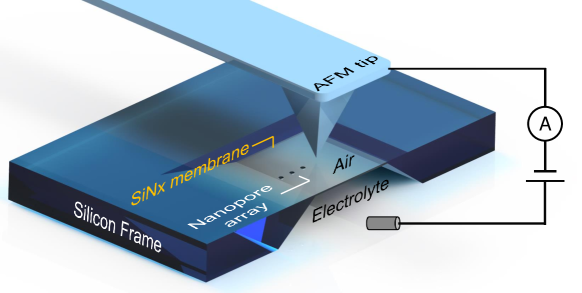
We have developed a new approach for forming solid-state pores that combines the positioning advantages of particle beam milling and the simplicity/low-cost of the electric breakdown approach with the powerful imaging capabilities of Atomic Force Microscopy (AFM). In our approach, which we call Tip-Controlled Local Breakdown (TCLB), a conductive AFM tip is brought into contact with a nitride membrane and used to apply a local voltage to the membrane (figure 1). The local voltage induces electric breakdown at a position on the membrane determined by the AFM tip, forming a nanopore at that location, which we demonstrate via I-V measurement, TEM characterization and single-molecule translocation. Firstly, in TCLB, the nanoscale curvature of the AFM tip (r 10 nm) localizes the electric field to a truly nanoscale region, eliminating the possibility of forming undesirable additional nanopores on the membrane as well as preventing the pore-free region of the membrane from being damaged by high electric fields. Secondly, TCLB can form pores with a spatial precision determined by the nanoscale positioning capability of the AFM instrument (an improvement in spatial precision from micro to nanoscale). Thirdly, TCLB drastically shortens the fabrication time of a single nanopore from on order of seconds to on order of 10 ms (at improvement of at least 2 orders of magnitude). Fast pore fabrication implies that arrays can be written with extremely high throughput (over 100 pores in a half an hour, compared to in a day 28). Fourthly, as TCLB is AFM based, it can harness the topographic, chemical and electrostatic scanning modalities of an AFM to image the membrane before and after pore formation, enabling precise alignment of pores to existing features. The scanning capabilities of the AFM tool can be used to automate fabrication of arrays of precisely positioned pores, with the successful fabrication of each pore automatically verified by current measurement at the tip following voltage application. The precise control of the contact force, made possible by AFM, is essential for establishing the reliable contact between the tip and the membrane. As AFM are benchtop tools that operate in ambient conditions (e.g. at atmospheric pressure and normal indoor humidity) they are inherently low-cost and can be readily scaled. The ability to work in ambient conditions implies that the approach is compatible with materials possessing sensitive which require chemical functionalization (e.g. that might be damaged by vacuum conditions used in FIB and TEM). Finally, while classic dielectric breakdown requires that both sides of the membrane be in contact with aqueous electrolyte reservoirs, our approach requires that only one side of the membrane be in contact with a liquid reservoir, considerably easing the scaling of our method and the speed of nanopore formation, as the AFM scanning takes place in a dry environment.
2 Results
2.1 Nanopore Fabrication
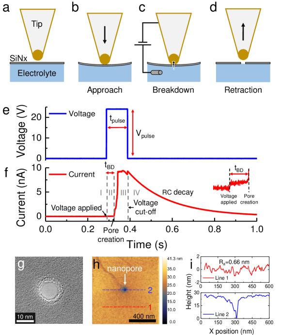
The schematic of the experimental setup is illustrated in figure 1. Using a bench-top AFM setup operated in ambient laboratory conditions, a conductive AFM tip is brought into contact with a thin nitride membrane sitting on top of an electrolyte reservoir. The conductive AFM tip is positioned a distance of 100 m from the membrane (figure 2 a). To initiate pore fabrication, the tip approaches the membrane at a speed of 5 m/s until it engages with the surface (figure 2 b). A small loading force (typically in the order of 1 nN) is applied to the tip in order to minimize contact resistance between the tip and the membrane. This force is set sufficiently small to avoid tip-induced mechanical damage to the membrane. To initiate the breakdown process, the tip is positioned at the desired location in the scanning region and a single rectangular pulse is applied (figure 2 d). The pulse has an amplitude of , and a duration of . The applied voltage pulse initiates the breakdown process and creates a nanoscale pore on the membrane, located at the tip location. After nanopore formation, the tip is retracted from the membrane (figure 2 d). A representative breakdown event is shown in figure 2 e-g. A voltage pulse of =24 V, =100 ms is applied (figure 2 e). After voltage application, the current increases to 50 pA and remains roughly constant (figure 2 f inset). After a time delay of =36.2 ms (figure 2 f), the current increases sharply to a few nA, indicating successful breakdown and nanopore formation. If the pores are large, successful nanopore fabrication at the tip location can additionally be confirmed by a subsequent topographic AFM scan (figure 2 h,i). When the nanopore diameter is smaller or comparable (d10 nm) to the tip radius of curvature, the nanopore may not be observed in the AFM scan.
We have developed a custom script enabling automatic control of the pore fabrication process. Using this script we can readily create pore arrays, iterating the single-pore formation process over a grid with the pores spaced evenly by 500 nm. Using the same tip, we have successfully fabricated over 300 nanopores on the same membrane, demonstrating the scalability of our TCLB technique (see supplementary S2 for more information).
2.2 Probing the breakdown threshold
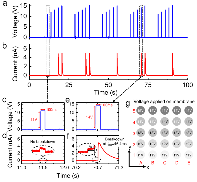
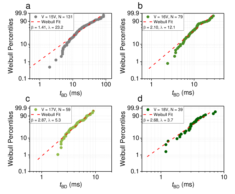
Our automated pore fabrication protocol enables efficient varying of process parameters to optimize pore fabrication. In particular, we vary the pulse amplitude across the nanopore array to probe the threshold at which membrane breakdown occurs. A pulse train of five subsets, with each set containing five rectangular pulses of fixed duration (100 ms) but increasing amplitude (11 V to 15 V, with an increment of 1 V), are applied across the membrane (figure 3 a, blue trace). Each pulse is applied to a different location on the membrane. The detected current is shown in Figure 3 b (trace in red). The locations are arrayed spatially in a square grid, with the pulse location in the array given by figure 3 g. The fabrication process starts from location A1 and ends at location E5, rastering in the direction (figure 3 g, A1A5, B1B5, C1C5, D1D5, E1E5). The spacing between each fabrication site is 500 nm. Spikes in the detected current, which occur for pulse amplitudes greater than V, indicate successful electric breakdown. At =14 V, 2 out of 5 attempts induce breakdown. A further increase of the voltage to 15 V leads to a 100% breakdown probability (5 out of 5). Magnified view of no-breakdown and successful breakdown events are shown in figure 3 (c-f) corresponding to location A1 (=11 V) and D4 (=14 V).
2.3 TEM characterization
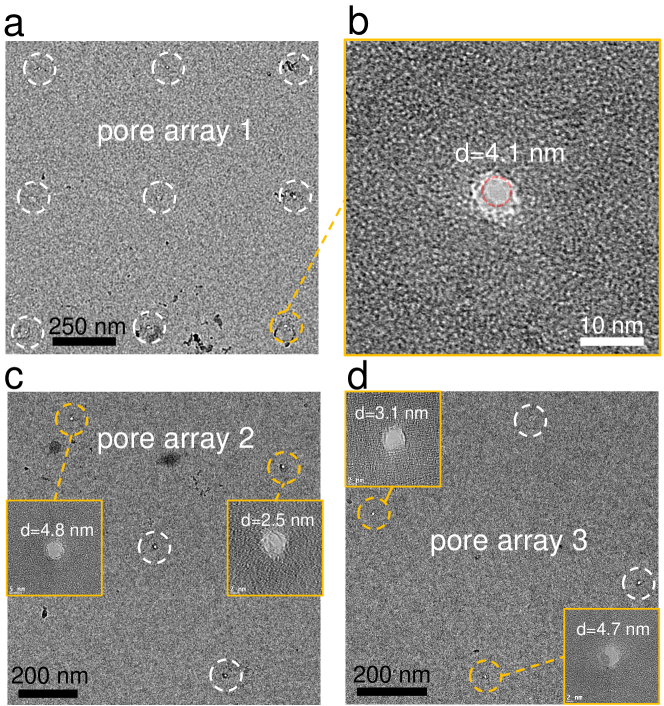
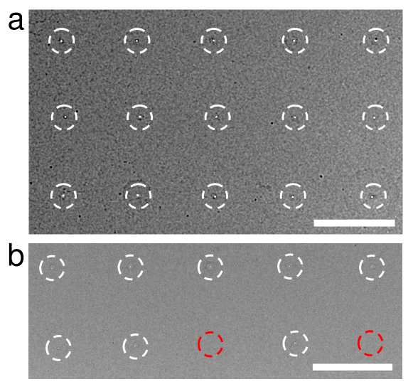
TEM microscopy allowed for a detailed characterization of the nanopores made by TCLB. Figure 4 shows three TEM micrographs of nanopore arrays. In agreement with our AFM settings (figure 2 j and figure 3 g), nanopores are spaced evenly by 500 nm in an array format. Figure 4 a and b show a 33 nanopore array fabricated using = 15 V, = 100 ms. Figure 4 c and d show two nanopore arrays made on a new membrane with a new tip under exactly the same fabrication conditions (= 15 V, = 100 ms). Despite using different tips and membranes (12-14 nm thick) from different chips, nanopores fabricated with the same parameters as our TCLB method have similar diameters (below or close to 5 nm).
2.4 Pore Formation Mechanism
2.4.1 Weibull versus Log-normal
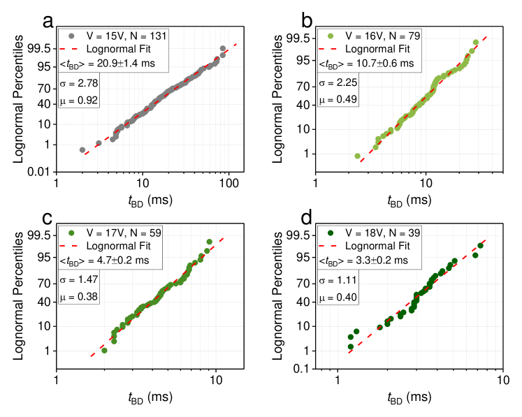
Nanopore fabrication time (time-to-breakdown, ) can provide insight into the pore formation mechanism. Nanopores fabricated via classic dielectric breakdown have a time-to-breakdown following a Weibull probability distribution 29, 28, 30. The Weibull distribution is used extensively to model the time-to-failure of semiconductor devices 31, 32. The Weibull distribution arises from the “weakest-link” nature of typical dielectric breakdown process, where breakdown happens at the weakest position over a large membrane area. The nanopore fabrication time is dominated by the time to make a pore at this weakest position.
In contrast, we find that our time-to-breakdown distribution, obtained from forming over 300 nanopores using our automatic process, yields better agreement with a log-normal probability distribution. Figure 5 shows the cumulative distribution of time-to-breakdown plotted with a log-normal scaling. In this form, data distributed according to a log-normal distribution follows a straight line. Our time-to-breakdown results, linearized by this rescaling, are thus clearly consistent with a log-normal distribution. In figure S4, we plot the same results rescaled appropriately for a Weibull, and it is apparent that the Weibull is not as good a description. See supplementary materials section 4 for more detail on log-normal, Weibull distribution and appropriate rescalings (probability plot forms).
The better agreement with a log-normal suggests that the physical mechanism of pore-formation is different using TCLB than classic breakdown. Under tip control, the membrane location where dielectric breakdown occurs is controlled by the tip position, and is thus highly defined rather than random. In this case the statistics of membrane breakdown is no longer a weakest link problem (i.e. determined by the time to breakdown of some randomly located “weak-point”), but instead is determined by the degradation of a “typical” location on the membrane reflecting average film properties. Theoretical and experimental work demonstrate that the overall time-scale of a degradation process that arises from the multiplicative action of many small degradation steps (regardless of physical mechanism) can be modelled via a log-normal distribution 33, 34, 35, 36. Possible degradation mechanisms for our pore-formation process include electromigration, diffusion and corrosion 37.
2.4.2 Voltage dependence of time-to-breakdown
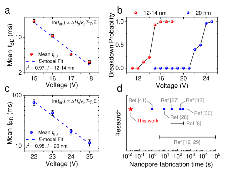
In figure 6 a we show the mean time-to-breakdown () versus voltage on a semi-log scale. The mean time-to-breakdown decreases exponentially with voltage. This behaviour is predicted by the E-model of time dependent dielectric breakdown (TDDB) 38, which predicts that the mean time-to-breakdown should depend exponentially on the local electric field (proportional to applied voltage at the tip). The E-model arises fundamentally from a thermochemical 38, 39 rather than a direct tunnelling mechanism (Fowler-Nordheim tunnelling) 40. In thermochemical breakdown, high voltage across the dielectric material induces strong dipolar coupling of local electric field with intrinsic defects in the dielectric. Weak bonding states can be thermally broken due to this strong dipole-field coupling, which in turn serves to lower the activation energy required for thermal bond-breakage and accelerates the degradation process, resulting in a final dielectric breakdown 38, 39.
We have also investigated whether we can use tip-controlled breakdown to produce pores in thicker (20 nm) nitride membranes. We are able to form pores with a high probability but with a corresponding increase in the required voltage, as demonstrated by figure 6b. The mean time-to-breakdown as a function of voltage in the thicker membranes also follow the E-model (figure 6 c).
In figure 6d we compare the average time-to-breakdown for our tip controlled approach versus classical dielectric breakdown. We find that our approach gives pore formation times two orders of magnitude lower than classical breakdown, by comparison with a wide-range of experimental studies 19, 29, 41, 8, 28, 27, 30, 42, 43 exploring classical breakdown for different film thickness (10-30 nm, 75 nm), pH (2-13.5) and voltage (1-24 V).
2.5 Single Molecule DNA Detection
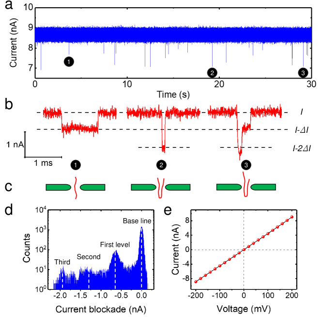
Lastly, we show nanopores produced using our tip-controlled approach can be used for single molecule detection. Figure 7 shows results for 100 bp ladder DNA (100-2000 bp) translocating through a 9.9 nm pore (=20 V, =150 ms, membrane thickness 10 nm, tip radius =105 nm). To perform single molecule detection, the chip is transferred to a fluidic cell with DNA containing 1 M KCl buffer added to the chamber and DNA-free buffer added to the chamber. A potential drop of 200 mV is applied across the nanopore, so that DNA molecule are pulled from to through the pore. Figure 7 a-b shows typical signatures of ionic blockades induced by translocating DNA, composed of a mixture of single and multi-level events. A histogram of current blockades, including 587 translocation events measured by the same nanopore, is shown in Figure 7 d. Prior to performing this DNA translocation experiment, an I-V trace was obtained to characterize pore size (figure 7 e), which yielded a nanopore resistance of 23.0 M. This strong linearity between current and applied voltage demonstrates that our TCLB fabricated nanopore has an outstanding Ohmic performance. Using a membrane thickness =10 nm and an electrolyte conductivity =10 S/m, according to the pore conductance model44 the estimated effective pore diameter is 9.9 nm.
3 Discussion and Conclusion
In summary, we show that tip-controlled local breakdown can be used to produce pores with nm positioning precision (determined by AFM tip), high scalability (100’s of pores over a single membrane) and fast formation (100 faster than classic breakdown) using a bench-top tool. These capabilities will greatly accelerate the field of solid-state nanopore research. In particular, the nm positioning is crucial for wide-range sensing and sequencing applications where there is a need to interface nanopores with additional nanoscale elements. Sequencing approaches based on tunneling require positioning a pore between two electrodes 4, 5. Plasmonic devices with interfaced pores require positioning pores at the optimal distance ( nm) from nano antennas in order to maximize plasmonic coupling 6, 7, 8, 9, 10. In devices utilizing nanofluidic confinement (e.g. nanochannels, nanocavities) pores need to be aligned with etched sub 100 nm features 11, 12, 13, 45. In addition to producing pores, our AFM based approach can exploit multiple scanning modalities (topographic, chemical, electrostatic) to map the device prior to pore production and so align pores precisely to existing features.
TCLB can be integrated into an automated wafer-scale AFM system, ensuring nm alignment of each pore with simultaneous mass pore production. Thus, not only can TCLB drive novel nanopore sensing applications, TCLB can simultaneously drive the industrial scaling of these applications. As an example, consider combining TCLB with photo-thermally assisted thinning42, 46, 27. In a photo-thermally assisted thinning process, a laser beam is focused on a silicon nitride membrane, leading to formation of a locally thinned out region, with thinning achieved down to a few nm 42. If there is only one thinned well formed, classic dielectric breakdown will tend to form a pore at this ‘thinned out’ weakest position. Classic dielectric breakdown, however, is limited to forming only one pore in one well across an entire membrane. In contrast, TCLB can position pores in each member of a large-scale array of photo-thermally thinned wells, with the wells packed as close as the photo-thermal thinning technique allows. Specifically, AFM topographic scans will determine the center-point of each well and TCLB will then form pores at these positions.
TCLB may also have applications beyond nanopore fabrication, providing an AFM-based approach to locally characterize the dielectric strength of thin membranes and 2D materials. This application, which could be useful for the MEMS and the semiconductor industry, could enable mapping of dielectric strength across large membranes and semiconductor devices, leading to enhanced material performance (e.g. for high- gate dielectrics 47).
4 Methods
Materials. The nitride membranes we use are commercially available from Norcada (part # NBPT005YZ-HR and NT002Y). The membrane is supported by a circular silicon frame (2.7 m diameter, 200 m thickness) with a window size of 1010, 2020 or 5050 m2. The membrane thickness is 10 nm, 12-14 nm or 20 nm. The AFM probes used are obtained from Adama Innovations (part # AD-2.8-AS) and have a tip radii of curvature of 105 nm. Nanopore fabrication experiments are performed in 1 M sodium percholorate dissolved in propylene carbonate (PC), with a conductivity of 2.82 S/m 48. DNA translocation experiments are performed in a 3D printed fluidic cell with 100 bp ladder DNA (Sigma-Aldrich, 100-2000 bp) diluted to a final concentration of 0.5 g/mL in 1 M KCl buffered with 10 mM Tris and 1 mM EDTA at pH=8.0.
Instrumentation. The atomic force microscope used in our experiments is a MultiMode Nanoscope III from Digital Instruments (now Bruker). Nanoscript is used for automated fabrication of nanopores. The TEM images are acquired using the JEM-2100F TEM from JEOL.
Current Data Acquisition and Analysis. The current signal during nanopore fabrication is recorded using a custom current amplifier with 5 kHz detection bandwidth. Analysis of dielectric breakdown events in the current signal was performed using a custom Python code. The ionic trans-pore current during DNA translocations was recorded using an Axopatch 200B with a 250 kHz sampling rate, low-pass filtered at 100 kHz. DNA translocation data analysis was carried out using Transalyzer49.
This work is financially supported by the Natural Sciences and Engineering Research Council of Canada (NSERC) Discovery Grants Program (Grant No. RGPIN 386212 and RGPIN 05033), Idea to Innovation (I2I) Grant (I2IPJ 520635-18) and joint CIHR funded Canadian Health Research Projects grant (CIHRR CPG-140199). The authors acknowledge useful discussions with Prof. Robert Sladek and Hooman Hosseinkhannazer. The authors acknowledge Norcada for material supplies (nitride membranes). The authors acknowledge Facility for Electron Microscopy Research (FEMR) at McGill and Centre de Caractérisation Microscopique des Matériaux (CM)2 at Ecole Polytechnique de Montréal for access to electron microscopes.
4.1 S1-Experimental Setup
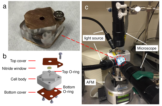
Here we discuss the detailed experimental setup for TCLB nanopore fabrication. The fluidic cell assembly and accompanying schematic are shown in figure S1 a and b. Prior to pore fabrication, the circular nitride TEM window is mounted in the fluidic cell with the cell body filled by electrolyte. The cell is then placed inside the AFM headstage (figure S1 c). Alignment of the conductive AFM tip to the nitride membrane is monitored via two optical microscopes with an external light source.
4.2 S2-Reliability and scalability of TCLB
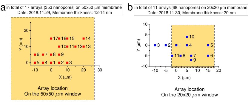
To demonstrate the reliability and scalability of the TCLB technique, we fabricated over 300 nanopores using the same AFM tip on one membrane. All data presented in figure 5 are collected from a total of 308 nanopores, fabricated using a single tip on the same membrane window (12-14 nm thick, window size 5050 m2) with a total time of around 30 min. The location of the arrays (17 in total) in relation to the window position are mapped out in figure S2 a. Each array contains a maximum possible of 25 nanopores (55 array). Figure S2 b shows another example of 11 arrays (in total 68 nanopores) located on a 20 nm thick membrane, window size 2020 m2.
4.3 S3-TEM characterization
Two additional TEM micrographs of nanopore arrays are presented in figure S3.
4.4 S4-Log-normal distribution and Weibull distribution
The probability density function (pdf) and cumulative distribution function (cdf) of log-normal distribution and 2-parameter Weibull distribution are given by:
Log-normal pdf:
| (S1) |
Log-normal cdf:
| (S2) |
Weibull pdf:
| (S3) |
Weibull cdf:
| (S4) |
where , are log-normal distribution’s shape and scale parameters; and are Weibull distribution’s shape and scale parameters. The symbol erf designates the error function, . F(t) is the cumulative failure rate at time t (t0).
Probability plots of log-normal and Weibull
The probability plots of distributions are constructed by rescaling the axes to linearize the cumulative distribution function (cdf) of the distribution. For example after rescaling both X axis and Y axis, a log-normal distribution will show up as a straight line in the log-normal probability plot, likewise a Weibull distribution will show up as a straight line in the Weibull probability plot. The X scale type and Y scale type for log-normal probability plot and Weibull probability plot are given by:
| Distribution | X scale type | Y scale type |
|---|---|---|
| Log-normal | Ln | Probability |
| Weibull | Log10 | Double Log Reciprocal |
where Probability scaling is given by the inverse of a cumulative Gaussian distribution: . The quantity is the cumulative Gaussian distribution function, . Double log reciprocal scaling is given by .
An example of the log-normal probability plot of time-to-breakdown () is shown in figure 5. An example of the Weibull probability plot for the same data set is shown in figure S4. One can compare probability plots for log-normal and Weilbull and conclude that the time-to-breakdown () fits better to a log-normal distribution.
4.5 S5-Nanopore fabrication time comparison
The following table compares dielectric breakdown based nanopore fabrication approaches in greater detail, including average pore fabrication time, membrane thickness, breakdown voltage, min/max fabrication time and number of nanopores analyzed.
| Methods |
|
|
|
|
|
|||||||||||
|---|---|---|---|---|---|---|---|---|---|---|---|---|---|---|---|---|
| This work | 20 ms | 10 nm, 12-14 nm, 20 nm | 13-25 V | 1 ms | 85 ms | 400 | ||||||||||
| CBD 19, 29 | NA | 10 nm, 30 nm | 5-17 V | 4 s | 105 s | 50 | ||||||||||
| Micro pipette 28 | 8.9 s | 10 nm | up to 24 V | 1 s | 17 s | 169 | ||||||||||
| Two-step BD 30 | 265.5 s | 20 nm | 10, 20 V | 150 s | 350 s | 50 | ||||||||||
|
1 s | 10 nm | 2.5, 7 V | 0.1 s | 20 s | 40 | ||||||||||
|
NA | 20 nm | 6 V | 30 s | 300 s | NA | ||||||||||
|
35 s | 30 nm | 18 V | 10 s | 80 s | 33 | ||||||||||
|
165 s | 75 nm | 1 V | NA | NA | 29 | ||||||||||
4.6 S6-Nanopore PSD
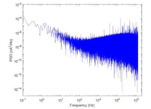
Figure below shows the current power spectral density (PSD) plot of the nanopore presented in figure 7.
References
- Clarke et al. 2009 Clarke, J.; Wu, H.-C.; Jayasinghe, L.; Patel, A.; Reid, S.; Bayley, H. Nature nanotechnology 2009, 4, 265
- Lindsay 2016 Lindsay, S. Nature nanotechnology 2016, 11, 109
- Miles et al. 2013 Miles, B. N.; Ivanov, A. P.; Wilson, K. A.; Doğan, F.; Japrung, D.; Edel, J. B. Chemical Society Reviews 2013, 42, 15–28
- Gierhart et al. 2008 Gierhart, B. C.; Howitt, D. G.; Chen, S. J.; Zhu, Z.; Kotecki, D. E.; Smith, R. L.; Collins, S. D. Sensors and Actuators B: Chemical 2008, 132, 593–600
- Ivanov et al. 2010 Ivanov, A. P.; Instuli, E.; McGilvery, C. M.; Baldwin, G.; McComb, D. W.; Albrecht, T.; Edel, J. B. Nano letters 2010, 11, 279–285
- Jonsson and Dekker 2013 Jonsson, M. P.; Dekker, C. Nano letters 2013, 13, 1029–1033
- Nicoli et al. 2014 Nicoli, F.; Verschueren, D.; Klein, M.; Dekker, C.; Jonsson, M. P. Nano letters 2014, 14, 6917–6925
- Pud et al. 2015 Pud, S.; Verschueren, D.; Vukovic, N.; Plesa, C.; Jonsson, M. P.; Dekker, C. Nano letters 2015, 15, 7112–7117
- Belkin et al. 2015 Belkin, M.; Chao, S.-H.; Jonsson, M. P.; Dekker, C.; Aksimentiev, A. ACS nano 2015, 9, 10598–10611
- Shi et al. 2018 Shi, X.; Verschueren, D.; Pud, S.; Dekker, C. Small 2018, 14, 1703307
- Zhang and Reisner 2015 Zhang, Y.; Reisner, W. Nanotechnology 2015, 26, 455301
- Zhang et al. 2018 Zhang, Y.; Liu, X.; Zhao, Y.; Yu, J.-K.; Reisner, W.; Dunbar, W. B. Small 2018, 14, 1801890
- Liu et al. 2018 Liu, X.; Zhang, Y.; Nagel, R.; Reisner, W.; Dunbar, W. B. arXiv preprint arXiv:1811.11105 2018,
- Tahvildari et al. 2015 Tahvildari, R.; Beamish, E.; Tabard-Cossa, V.; Godin, M. Lab on a Chip 2015, 15, 1407–1411
- Storm et al. 2003 Storm, A.; Chen, J.; Ling, X.; Zandbergen, H.; Dekker, C. Nature materials 2003, 2, 537
- Lo et al. 2006 Lo, C. J.; Aref, T.; Bezryadin, A. Nanotechnology 2006, 17, 3264
- Yang et al. 2011 Yang, J.; Ferranti, D. C.; Stern, L. A.; Sanford, C. A.; Huang, J.; Ren, Z.; Qin, L.-C.; Hall, A. R. Nanotechnology 2011, 22, 285310
- Xia et al. 2018 Xia, D.; Huynh, C.; McVey, S.; Kobler, A.; Stern, L.; Yuan, Z.; Ling, X. S. Nanoscale 2018, 10, 5198–5204
- Kwok et al. 2014 Kwok, H.; Briggs, K.; Tabard-Cossa, V. PloS one 2014, 9, e92880
- Briggs et al. 2014 Briggs, K.; Kwok, H.; Tabard-Cossa, V. Small 2014, 10, 2077–2086
- Jiang et al. 2010 Jiang, Z.; Mihovilovic, M.; Chan, J.; Stein, D. Journal of Physics: Condensed Matter 2010, 22, 454114
- Saha et al. 2011 Saha, K. K.; Drndic, M.; Nikolic, B. K. Nano letters 2011, 12, 50–55
- Pud et al. 2016 Pud, S.; Chao, S.-H.; Belkin, M.; Verschueren, D.; Huijben, T.; van Engelenburg, C.; Dekker, C.; Aksimentiev, A. Nano letters 2016, 16, 8021–8028
- Carlsen et al. 2017 Carlsen, A. T.; Briggs, K.; Hall, A. R.; Tabard-Cossa, V. Nanotechnology 2017, 28, 085304
- Zrehen et al. 2017 Zrehen, A.; Gilboa, T.; Meller, A. Nanoscale 2017, 9, 16437–16445
- Wang et al. 2018 Wang, Y.; Ying, C.; Zhou, W.; de Vreede, L.; Liu, Z.; Tian, J. Scientific reports 2018, 8, 1234
- Ying et al. 2018 Ying, C.; Houghtaling, J.; Eggenberger, O. M.; Guha, A.; Nirmalraj, P.; Awasthi, S.; Tian, J.; Mayer, M. ACS nano 2018, 12, 11458–11470
- Arcadia et al. 2017 Arcadia, C. E.; Reyes, C. C.; Rosenstein, J. K. ACS nano 2017, 11, 4907–4915
- Briggs et al. 2015 Briggs, K.; Charron, M.; Kwok, H.; Le, T.; Chahal, S.; Bustamante, J.; Waugh, M.; Tabard-Cossa, V. Nanotechnology 2015, 26, 084004
- Yanagi et al. 2018 Yanagi, I.; Hamamura, H.; Akahori, R.; Takeda, K.-i. Scientific reports 2018, 8
- Dissado et al. 1984 Dissado, L.; Fothergill, J.; Wolfe, S.; Hill, R. IEEE Transactions on electrical insulation 1984, 227–233
- Degraeve et al. 1995 Degraeve, R.; Groeseneken, G.; Bellens, R.; Depas, M.; Maes, H. E. A consistent model for the thickness dependence of intrinsic breakdown in ultra-thin oxides. Electron Devices Meeting, 1995. IEDM’95., International. 1995; pp 863–866
- Peck and Zierdt 1974 Peck, D. S.; Zierdt, C. Proceedings of the IEEE 1974, 62, 185–211
- Berman 1981 Berman, A. Time-zero dielectric reliability test by a ramp method. Reliability Physics Symposium, 1981. 19th Annual. 1981; pp 204–209
- Lloyd et al. 2005 Lloyd, J.; Liniger, E.; Shaw, T. Journal of Applied Physics 2005, 98, 084109
- McPherson 2010 McPherson, J. W. Reliability physics and engineering; Springer, 2010
- Strong et al. 2009 Strong, A. W.; Wu, E. Y.; Vollertsen, R.-P.; Sune, J.; La Rosa, G.; Sullivan, T. D.; Rauch III, S. E. Reliability wearout mechanisms in advanced CMOS technologies; John Wiley & Sons, 2009; Vol. 12
- McPherson and Mogul 1998 McPherson, J.; Mogul, H. Journal of Applied Physics 1998, 84, 1513–1523
- McPherson et al. 2003 McPherson, J.; Kim, J.; Shanware, A.; Mogul, H. Applied Physics Letters 2003, 82, 2121–2123
- McPherson et al. 1998 McPherson, J.; Reddy, V.; Banerjee, K.; Le, H. Comparison of E and 1/E TDDB models for SiO/sub 2/under long-term/low-field test conditions. Electron Devices Meeting, 1998. IEDM’98. Technical Digest., International. 1998; pp 171–174
- Yanagi et al. 2014 Yanagi, I.; Akahori, R.; Hatano, T.; Takeda, K.-i. Scientific reports 2014, 4, 5000
- Yamazaki et al. 2018 Yamazaki, H.; Hu, R.; Zhao, Q.; Wanunu, M. ACS nano 2018, 12, 12472–12481
- Bandara et al. 2019 Bandara, Y. N. D.; Karawdeniya, B. I.; Dwyer, J. R. ACS Omega 2019, 4, 226–230
- Kowalczyk et al. 2011 Kowalczyk, S. W.; Grosberg, A. Y.; Rabin, Y.; Dekker, C. Nanotechnology 2011, 22, 315101
- Larkin et al. 2017 Larkin, J.; Henley, R. Y.; Jadhav, V.; Korlach, J.; Wanunu, M. Nature nanotechnology 2017, 12, 1169
- Gilboa et al. 2018 Gilboa, T.; Zrehen, A.; Girsault, A.; Meller, A. Scientific reports 2018, 8, 9765
- Okada et al. 2007 Okada, K.; Ota, H.; Nabatame, T.; Toriumi, A. Dielectric breakdown in high-K gate dielectrics-Mechanism and lifetime assessment. Reliability physics symposium, 2007. proceedings. 45th annual. ieee international. 2007; pp 36–43
- D’Aprano et al. 1996 D’Aprano, A.; Salomon, M.; Iammarino, M. Journal of electroanalytical chemistry 1996, 403, 245–249
- Plesa and Dekker 2015 Plesa, C.; Dekker, C. Nanotechnology 2015, 26, 084003