Large positive magneto-conductivity at microwave frequencies
in the compensated topological insulator BiSbTeSe2
Abstract
The bulk electronic properties of compensated topological insulators are strongly affected by the self-organized formation of charge puddles at low temperature, but their response in the microwave frequency range is little studied. We employed broadband impedance spectroscopy up to 5 GHz to address the ac transport properties of well-compensated BiSbTeSe2, where charge puddles are known to form as metallic entities embedded in an insulating host. It turns out that the average puddle size sets the characteristic frequency in the GHz range, across which the insulating dc behavior is separated from a metal-like high-frequency response of delocalized carriers within the puddles. This is found to be controlled by a magnetic field, giving rise to a large positive magneto-conductivity observable only in the GHz range. This curious phenomenon is driven by the Zeeman energy which affects the local band filling in the disordered potential landscape to enhance the puddle size.
One of the most prominent features of topological insulators is the spin-momentum locking in the surface states Ando13 , which is particularly useful for spintronic applications Pesin12 . To efficiently utilize the spin-momentum-locked surface states in applications, one should get rid of the residual bulk conduction, and this has been achieved by carefully compensating residual donors by residual acceptors through composition tuning in the BixSb2-xTeySe3-y compound Ando13 ; Taskin11 ; Ren11 . Although such compensated topological insulators show reasonably high bulk insulation in dc, it has been elucidated that their transport properties are not only determined by the topologically protected surface states but also by the presence of charge puddles in the bulk Skinner12 , particularly at finite frequencies up to the infrared range Borgwardt16 . This is because the Coulomb disorder of the randomly distributed charged donors and acceptors gives rise to potential fluctuations which grow as in a volume of size Skinner12 ; Shklovskii72 ; this inevitably leads to the self-organized formation of charge puddles on a mesoscopic length scale at low temperatures. On this length scale, portions of a sample contain delocalized charge carriers which give rise to a Drude-like contribution to the optical conductivity above the Thouless cut-off frequency = Borgwardt16 . This cut-off is given by the time scale needed to diffuse through a puddle with the diffusion constant . Using a simple scaling argument Skinner12 ; Shklovskii72 , nm is expected on the basis of infrared data Borgwardt16 . This corresponds to in the GHz range.
Since the current-day information technology operates in the GHz range, understanding the microwave response of topological-insulator materials would be of crucial importance for their future applications in spintronics; nevertheless, the role of puddles in the transport properties in the GHz range has not yet been studied. This work is conceived to address this lack of understanding.
At low temperature, the Drude-like puddle contribution to and its discrepancy with the dc conductivity have been observed in the well-compensated compound BiSbTeSe2 by Borgwardt et al. Borgwardt16 , who focused on infrared frequencies above the phonon range. Clear evidence for puddles stems in particular from the characteristic temperature-driven suppression of this Drude-like contribution on a temperature scale = set by the average Coulomb interaction between neighboring dopants Borgwardt16 . This “evaporation” of puddles is caused by thermally activated carriers which screen the Coulomb disorder. In BiSbTeSe2, = K was observed Borgwardt16 ; Knispel17 . Also, puddles can explain the coexistence of electron-type and hole-type carriers in compensated samples Rischau16 and the small activation energy observed in dc resistivity data Skinner12 . Intriguingly, puddles are further found to be responsible for the surprising effect of gigantic negative magnetoresistance reported for TlBi0.15Sb0.85Te2 Breunig17 . In this context, novel magnetic-field effects would be expected in the vicinity of the cut-off frequency .
In this manuscript, we report on broadband spectroscopic investigations of BiSbTeSe2 in the cut-off frequency range to look for the ac conductivity behavior associated with charge puddles and their response to magnetic fields. Our central result is the discovery of a large positive magneto-conductivity at microwave frequencies, which arises due to the change of the puddle size by an external magnetic field. In addition, our data provide solid understanding of the role of puddles in the transport properties in the GHz range, providing foundations for future high-frequency applications of topological insulators.
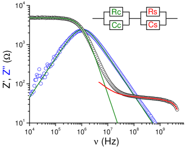
Single crystals of BiSbTeSe2 were grown from a melt of high-purity starting elements Bi, Sb, Te, and Se by using a modified Bridgman method in a sealed quartz-glass tube as described elsewhere Ren11 . For the microwave measurements, we used scotch-tape-cleaved flakes with length mm, width mm, and thickness m; the possible error in the determination of leads to an uncertainty in the absolute values of about 10 %. The measurements were performed in a commercial 4He-flow cryo-magnet (Quantum-Design PPMS) employing four point geometry for the dc measurements and a home-made, two point coaxial-line inset for the microwave range. The complex frequency-dependent conductivity = was measured using a coplanar waveguide setup for frequencies up to 5 GHz evaluating the complex scattering coefficients and gained via a vector network analyzer (ZNB8, Rohde&Schwarz). All measurements were performed with the electric field perpendicular to the crystallographic axis. The contacts were applied using silver paint. The lower boundary of the microwave measurement range is set by the influence of the contact electrodes. At the contact interfaces, the formation of Schottky-type depletion layers can lead to Maxwell-Wagner type effects Maxwell91 giving an additional capacitive contribution and a serial contact resistance . Together, they form a element in series with the intrinsic sample impedance. The contacts thus are short-cut for frequencies Lunkenheimer02 ; Niermann12 . This allows us to reliably evaluate the intrinsic sample conductivity for frequencies above 30 MHz, as illustrated in Fig. S1 of the Supplemental Material SM .
The length scale of puddle formation is connected to a time scale = on which the locally uncompensated carriers behave like free charges. For larger times or lengths, carrier motion is hindered by the puddle boundaries. This leads to insulating behavior for dc or low-frequency transport measurements and to a Drude-like metallic conductivity at high frequencies which is cut off below . Assuming that puddles form as soon as the fluctuations of the Coulomb potential are as large as , where denotes the band gap, Shklovskii and coworkers Skinner12 ; Shklovskii72 estimated via a simple scaling argument,
| (1) |
where is the defect density of acceptors and donors, and the average Coulomb interaction between neighboring dopants is given by = with the permittivity . For BiSbTeSe2, infrared data show = 0.26 eV and Borgwardt16 . Note that and thus also are sample-dependent quantities. For two different samples of BiSbTeSe2, = K and K were reported, resulting in = cm-3 and cm-3, respectively Borgwardt16 ; Knispel17 . This is equivalent to and nm. Using a diffusion constant of 2 cm2/s Borgwardt16 , we find 2 GHz. Note, however, that direct experimental values for or are still lacking.
Bömerich et al. Boemerich17 used a numerical approach combined with a refined scaling argument and found smaller values for the length scale . An experimental lower limit is provided by the length scale = nm observed for surface puddles by scanning tunnelling microscopy in BiSbTeSe2 Knispel17 . The Dirac carriers on the surface give rise to enhanced screening, one thus expects . Experimentally, the defect density may not only be sample dependent but it may also vary within a given sample. Thus, one has to expect a distribution of puddle sizes and concomitantly a distribution of cut-off frequencies, giving rise to a considerably broadened features in the dynamic response. For BiSbTeSe2, the above discussed limits of , nm and nm, span a broad frequency range of to GHz for the distribution of .
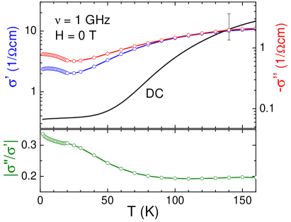
Clear fingerprints of puddle formation are found in the temperature dependence of the conductivity (Fig. 1). We observe the expected discrepancy between dc and ac conductivities at low temperature, while the high-temperature data agree within the experimental error bar. At the lowest measured temperatures, the dc conductivity lies more than one decade below the ac data measured at GHz. The contribution of puddles is most evident from the reincrease of the ac conductivity below roughly 30 K, which agrees with the energy scale found in the infrared data Borgwardt16 . Note that variable range hopping (VRH) also gives rise to an enhanced ac conductivity, which explains the behavior at higher temperatures. In BiSbTeSe2, VRH has been shown to describe the dc resistivity in a temperature window above about 80 K Ren11 . In the ac conductivity, VRH gives rise to a contribution to both and that scales with a power law with Lunkenheimer03 . This scaling behavior results in a fixed ratio over a wide range in temperature and frequency Jonscher96 ; Elliott87 . In BiSbTeSe2, we find such a constant ratio at 1 GHz above about 70 K, see bottom panel of Fig. 1. In contrast, the increase of at lower temperatures can be attributed to the formation of polarizable puddles with a finite cut-off frequency resulting in a considerable contribution to . This additional increase of is also evident in the top panel of Fig. 1.
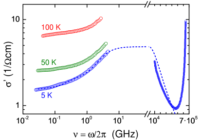
Figure 2 shows broadband microwave spectra of the conductivity for different temperatures. We observe an increase of with increasing below 5 GHz. Importantly, this increase is more pronounced at 5 K than at 50 K or 100 K, i.e., the frequency dependence is larger at a temperature where puddles have formed. The overall much larger value of at higher temperatures and its weaker frequency dependence correspond to the metallic Drude contribution of thermally activated carriers, as also observed in the infrared range Borgwardt16 . The low-temperature behavior can be attributed to a smeared-out cut-off of the Drude-like contribution of puddles at frequencies of the order of 1 GHz. To quantitatively analyse this behavior, we fitted the 5 K data by considering Drude-Lorentz oscillators, see dashed line in Fig. 2: In this fitting, the damping = THz was fixed to the value determined from the infrared data Borgwardt16 ; to take into account the distribution of the puddle size in which the charge carriers are confined, we approximated the situation as a sum of three broad Lorentzians centered at 9.3 GHz, 72 GHz, and 234 GHz (these frequencies are optimized to best reproduce the data). For such overdamped oscillators, this distribution gives an effective cut-off frequency GHz. Also, this distribution of the eigenfrequencies corresponds to a range of the puddle size of 0.1 – 3 m, when we use given in Ref. Borgwardt16 . One can see in Fig. 2 that this model reproduces both the low and high frequency behavior of reasonably well, giving confidence that the overall behavior of is governed by puddles.
An external magnetic field influences the size of puddles, as shown recently by Breunig et al. Breunig17 in the nearly bulk-insulating topological insulator TlBi0.15Sb0.85Te2 by dc resistivity measurements. Puddles form when the bands touch the chemical potential due to the spatial fluctuations of the Coulomb potential. The magnetic field does not change the Coulomb potential but the Zeeman energy shifts the band bottom/top with respect to the disordered potential landscape and thereby affects the puddle size Breunig17 . The compound TlBi0.15Sb0.85Te2 studied in Ref. Breunig17 is less well compensated than BiSbTeSe2 and the low-temperature conductivity is determined by percolating current paths formed in the disordered bulk. A field-induced change of the puddle size leads to a strong increase of percolating puddles and hence a gigantic field-induced reduction of the dc resistance Breunig17 . In contrast, BiSbTeSe2 is well compensated. Puddles do not percolate, the bulk resistivity at low temperatures is much higher, and the influence of a magnetic field on the dc conductivity is expected to be much weaker as long as the percolation limit is not reached. Close to the cut-off frequency, however, a magnetic-field-induced change of the puddle size may have considerable impact.
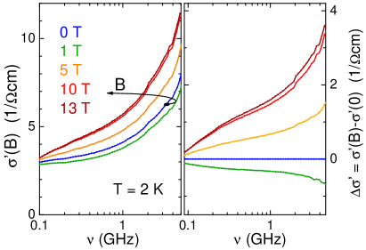
Figure 3 shows at 2 K for different values of the external magnetic field. One can see that the behavior at 1 T is clearly different from that at higher fields; namely, the conductivity in 1 T is lower than in zero field and the difference increases with increasing frequency, as is evident in the right panel. At such low fields, the ac transport is dominated by weak anti-localization (WAL) characteristic for disordered systems with strong spin-orbit coupling Altshuler81 ; Ando13 ; Hikami80 . The suppression of WAL in small magnetic fields leads to localization of carriers and therefore to a reduced conductivity. In contrast, in higher fields the conductivity increases strongly, in particular at higher frequencies. This can be attributed to a field-induced shift of the cut-off frequency that is triggered by a field-induced change of the puddle size. This shift is directly visualized in the left panel of Fig. 3 via the shift of the rise in .
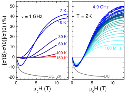
At high fields, the suppression of weak anti-localization still applies but it is overruled by the strong positive ac magneto-conductivity. This is evident in the left panel of Fig. 4, which depicts the normalized magneto-conductivity at 1 GHz as a function of the external magnetic field. The “dip” below 3 T is due to the WAL effect discussed above, but a pronounced positive magneto-conductivity sets in at higher fields. As shown in the right panel of Fig. 4, the high-field magneto-conductivity strongly increases with frequency, reaching 50% in 13 T at 4.9 GHz. The dc data shown in Fig. 4 for comparison is governed by the WAL all the way up to high fields and only presents negative magneto-conductivity approaching % at high magnetic field. This crossover in the high-field magneto-conductance from negative to positive upon changing from dc to the microwave range shows that it is not a field-induced percolation which dominates transport properties in compensated BiSbTeSe2. Rather, the magnetic field mainly affects the average size of still isolated puddles. The corresponding shift of the cut-off frequency naturally explains the large magneto-conductivity at frequencies in the vicinity of in the GHz range.
In the left panel of Fig. 4, one can also see how the magneto-conductivity behavior at 1 GHz changes with temperature. The pronounced positive microwave magneto-conductivity is limited to the low-temperature range where charge puddles are present. At higher temperatures ( 30 K) where puddles have evaporated, the magneto-conductivity is drastically suppressed.
In conclusion, we have demonstrated that the ac transport properties of the compensated topological insulator BiSbTeSe2 at low temperatures are determined by the presence of charge puddles, which gives rise to an unusual positive magneto-conductivity observable only in the GHz range. The random nature of the Coulomb-potential fluctuations causes a distribution of the puddle size, which leads to a broad cut-off regime in the microwave range separating the insulating dc behavior from the metal-like ac response; our analysis shows that the overall ac conductivity behavior points to the puddle-size distribution of 0.1 – 3 m. The remarkable effect of the magnetic field to enlarge the puddle size, previously suggested in Ref. Breunig17 for an imperfectly compensated topological insulator, is now found to cause a large positive magneto-conductivity even in a well-compensated system near the characteristic cut-off frequency. Hence, tailoring the defect density and the corresponding disorder-induced microstructure will be of crucial importance to any potential applications of bulk topological insulators in the technologically important GHz range.
Acknowledgements
The authors thank A. Rosch for valuable discussions. This work was funded by the Deutsche Forschungsgemeinschaft (DFG, German Research Foundation) – Project number 277146847 – CRC 1238 (projects A04 and B02).
References
- (1) Y. Ando, Topological insulator materials, J. Phys. Soc. Jpn 82, 102001 (2013)
- (2) D. Pesin and A. H. Macdonald, Spintronics and pseudospintronics in graphene and topological insulators, Nat. Mater. 11, 409 (2012).
- (3) A.A. Taskin, Z. Ren, S. Sasaki, K. Segawa, and Y. Ando, Observation of Dirac Holes and Electrons in a Topological Insulator, Phys. Rev. Lett. 107, 016801 (2011).
- (4) Z. Ren, A.A. Taskin, S. Sasaki, K. Segawa, and Y. Ando, Optimizing Bi2-xSbxTe3-ySey solid solutions to approach the intrinsic topological insulator regime, Phys. Rev. B 84, 165311 (2011).
- (5) B. Skinner, T. Chen, and B.I. Shklovskii, Why Is the Bulk Resistivity of Topological Insulators So Small?, Phys. Rev. Lett. 109, 176801 (2012).
- (6) N. Borgwardt, J. Lux, I. Vergara, Z. Wang, A.A. Taskin, K. Segawa, P.H.M. van Loosdrecht, Y. Ando, A. Rosch, and M. Grüninger, Self-organized charge puddles in a three-dimensional topological material, Phys. Rev. B 93, 245149 (2016).
- (7) B. I. Shklovskii and A. L. Efros, Completely Compensated Crystalline Semiconductor as a Model of an Amorphous Semiconductor, Sov. Phys. JETP 35, 610 (1972).
- (8) T. Knispel, W. Jolie, N. Borgwardt, J. Lux, Zhiwei Wang, Yoichi Ando, A. Rosch, T. Michely, and M. Grüninger, Charge puddles in the bulk and on the surface of the topological insulator BiSbTeSe2 studied by scanning tunneling microscopy and optical spectroscopy, Phys. Rev. B 96, 195135 (2017).
- (9) C.W. Rischau, A. Ubaldini, E. Giannini, and C.J. van der Beek, Charge puddles in a completely compensated topological insulator, New J. Phys. 18, 073024 (2016).
- (10) O. Breunig, Z. Wang, A.A. Taskin, J. Lux, A. Rosch, and Y. Ando, Gigantic negative magnetoresistance in the bulk of a disordered topological insulator, Nat. Comm. 8, 15545 (2017).
- (11) J.C. Maxwell, Treatise on Electricity and Magnetism, 3rd ed. (Dover, New York, 1991).
- (12) P. Lunkenheimer, V. Bobnar, A. V. Pronin, A. I. Ritus, A. A. Volkov, and A. Loidl Origin of apparent colossal dielectric constants, Phys. Rev. B 66, 052105 (2002).
- (13) D. Niermann, F. Waschkowski, J. de Groot, M. Angst, and J. Hemberger, Dielectric Properties of Charge-Ordered LuFe2O4 Revisited: The Apparent Influence of Contacts, Phys. Rev. Lett. 109, 016405 (2012).
- (14) See Supplemental Material at [URL] for supplemental data and discussions.
- (15) T. Bömerich, J. Lux, Q.T. Feng, and A. Rosch, Length scale of puddle formation in compensation-doped semiconductors and topological insulators, Phys. Rev. B 96, 075204 (2017).
- (16) P. Lunkenheimer and A. Loidl, Response of Disordered Matter to Electromagnetic Fields, Phys. Rev. Lett. 91, 207601 (2003).
- (17) A.K. Jonscher, Universal Relaxation Law (Chelsea, New York, 1996).
- (18) S.R. Elliott, A.c. conduction in amorphous chalcogenide and pnictide semiconductors, Adv. Phys. 36, 135 (1987).
- (19) A. Segura, V. Panchal, J. F. Sánchez-Royo, V. Marín-Borrás, V. Muñoz-Sanjosé, P. Rodríguez-Hernández, A. Muñoz, E. Pérez-González, F. J. Manjón, and J. González, Trapping of three-dimensional electrons and transition to two-dimensional transport in the three-dimensional topological insulator Bi2Se3 under high pressure, Phys. Rev. B 85, 195139 (2012).
- (20) B. Altshuler, A.G. Aronov, A.I. Larkin, and D.E. Khmel’nitskil, Anomalous magnetoresistance in semiconductors, Sov. Phys. JETP 54, 411 (1981).
- (21) S. Hikami, A. I. Larkin, and Y. Nagaoka, Spin-Orbit Interaction and Magnetoresistance in the Two Dimensional Random System, Prog. Theor. Phys. 63, 707 (1980).
Supplemental Material
Effect of Electrical Contacts
Schottky-type depletion layers tend to form at the electrical contact formed at interfaces between sample and silver electrodes. The depletion layers lead to Maxwell-Wagner type contributions to the complex impedance Maxwell91 . These can be modelled employing an equivalent circuit containing an additional capacitive contribution and a contact resistance . Together, they form an element in series with the intrinsic sample impedance. The resulting impedance thus can be described as
with the relaxation times and for contacts and sample, respectively. Usually, the thin contact depletion layers lead to and the contacts thus are short-cut for frequencies Lunkenheimer02 ; Niermann12 . In addition one can expand the accessible frequency range by subtracting the contact contribution, which dominates the low frequency range and therefore can be fitted for . The remaining impedance can be evaluated via the geometry factor with respect to the complex conductivity and .