Paramagnetic Meissner effect in voltage-biased proximity systems
Abstract
Conventional superconductors respond to external magnetic fields by generating diamagnetic screening currents. However, theoretical work has shown that one can engineer systems where the screening current is paramagnetic, causing them to attract magnetic flux—a prediction that has recently been experimentally verified. In contrast to previous studies, we show that this effect can be realized in simple superconductor/normal-metal structures with no special properties, using only a simple voltage bias to drive the system out of equilibrium. This is of fundamental interest, since it opens up a new avenue of research, and at the same time highlights how one can realize paramagnetic Meissner effects without having odd-frequency states at the Fermi level. Moreover, a voltage-tunable electromagnetic response in such a simple system may be interesting for future device design.
Introduction.—Conventional superconductors have two defining properties Tinkham (2004); Fossheim and Sudbø (2004). The first is their perfect conductance of electric currents, from which they derive their name. The second is the so-called Meissner effect, whereby dissipationless electric currents screen magnetic fields. Both properties arise due to a coherent condensate of electron pairs (Cooper pairs) which exhibits spontaneous symmetry breaking, and it is of fundamental interest to understand both in depth.
In bulk superconductors, the Meissner effect is diamagnetic, meaning that the screening currents try to expel magnetic flux from the superconductor. However, the story is more complicated in proximity structures, where superconductors and non-superconductors are combined to engineer novel device functionality. Diamagnetic screening in such structures has been investigated some while ago Zaikin (1982); Belzig et al. (1996), and several interesting impurity effects have been found Müller-Allinger et al. (1999); Belzig et al. (1999). A cylindrical geometry can increase the diamagnetic so-called overscreening Belzig et al. (2007). At ultra-low temperatures, a reentrant effect was observed experimentally Visani et al. (1990), and even an overall paramagnetic response in thermal equilibrium Müller-Allinger and Mota (2000). Other systems with unexpected properties are superconductor/ferromagnet (S/F) devices, where Cooper pairs can leak from S to F. The Cooper pairs of a conventional superconductor are singlet even-frequency pairs, i.e. they carry no net spin and respect time-reversal symmetry. Once they leak into F, some of these are converted into triplet odd-frequency pairs, which have fundamentally different properties Eschrig (2010); Blamire and Robinson (2014); Linder and Robinson (2015); Eschrig (2015); Buzdin (2005); Bergeret et al. (2005); Berezinskii (1974); Linder and Balatsky . One example is that odd-frequency pairs give rise to a paramagnetic Meissner effect, where the screening currents attract magnetic flux Linder and Balatsky ; Bergeret et al. (2001); Yokoyama et al. (2011); Asano et al. (2011); Mironov et al. (2012); Alidoust et al. (2014); Espedal et al. (2016). This effect has been predicted for a variety of S/F setups, and has been confirmed experimentally via muon-rotation experiments Di Bernardo et al. (2015). It has also been identified in e.g. metals with repulsive electron–electron interactions Fauchère et al. (1999) and at the interfaces of -wave superconductors Higashitani (1997); Löfwander et al. (2001). In these systems, the effect is caused by midgap states, which are again linked to odd-frequency pairing Linder and Balatsky .
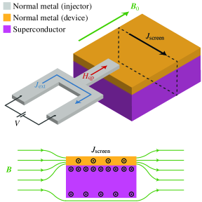
We consider a fundamentally different way of realizing the paramagnetic effect: by driving a superconductor/normal-metal (S/N) bilayer out of equilibrium via a voltage bias. Our suggested setup is visualized in Fig. 1, and explained in detail over the next two pages. The mechanism is again related to odd-frequency superconductivity; we will see that an essential ingredient is large subgap peaks in the normal-metal density of states (DOS), and these appear at energies where odd-frequency pairs dominate Tanaka et al. (2007); Linder and Balatsky . However, our setup does not require that these reside precisely at the Fermi level (midgap states). Instead, the Meissner response in our setup is determined by the DOS at a voltage-controlled finite energy. Our predictions can be verified via the same setup as Ref. Di Bernardo et al. (2015).
A related idea was discussed in Refs. Aronov (1973); Aronov and Spivak (1975), where they suggested that a microwave-irradiated superconductor might become paramagnetic. However, they concluded that the paramagnetic state would be unstable, and could therefore not be realized. In contrast, our system avoids this instability by realizing the paramagnetic effect in a proximity system instead of a bulk system. Moreover, voltage control may be more desirable than microwave control for potential applications.
A similar setup to ours was investigated in Ref. Bobkova and Bobkov (2013), where they calculated the Meissner response of S/N structures driven out of equilibrium using a voltage-controlled quasiparticle injector. However, they did not find a paramagnetic response, and the main reason appears to be their parameters. We analytically predict the effect for clean materials, thick superconductors, and low temperatures. In contrast, Ref. Bobkova and Bobkov (2013) considered dirty materials, thin superconductors, and high temperatures. This suppresses the subgap peaks in the DOS, which we will see are essential for a paramagnetic response.
Motivation.—Consider a superconducting system that is exposed to a weak magnetic field , which we describe via a vector potential . For concreteness, let us consider a geometry where a thin film at is subjected to a magnetic field , which we describe via the vector potential . This is identical to the experimental geometry employed in Ref. Di Bernardo et al. (2015). In the clean and nonlocal limits, the linear-response screening current is then given by
| (1) |
Here, we have introduced the screening kernel
| (2) |
where is the quasiparticle energy, the distribution function, the DOS, the Fermi-level DOS in the non-superconducting state, the Fermi velocity, and the electron charge. These equations are derived in standard textbooks on superconductivity Tinkham (2004); Schrieffer (1999), and have previously been used to e.g. predict paramagnetic effects in materials with repulsive electron interactions Fauchère et al. (1999), -wave superconductors Higashitani (1997), and microwave-irradiated superconductors Aronov (1973); Aronov and Spivak (1975). We provide a simple and compact derivation of this equation within the quasiclassical formalism in the Supplemental Material.
Many well-known results for Meissner effects can be seen directly from Eqs. 1 and 2. In equilibrium, the distribution has a Fermi–Dirac form, which at low temperatures reduces to a step function . Substituted into Eq. 2, this produces the simplified equation . For a BCS superconductor, there is a gap around the Fermi level , and causes . This produces a diamagnetic response. On the other hand, in systems with odd-frequency pairing, one can have a zero-energy peak in the DOS, and causes . This produces a paramagnetic response.
We are interested in a new way to realize the paramagnetic Meissner effect: by manipulating the distribution instead of the DOS . Before we discuss its exact physical origin, let us just assume that one can induce a two-step Fermi–Dirac-like distribution, which at low temperatures reduces to
| (3) |
We note that the effect of is essentially to excite electrons in the range and holes in the range , resulting in an excited energy mode or increased effective temperature. Substituting the above into Eq. 2, and using the electron–hole symmetry of the DOS , we get
| (4) |
In other words, if we can tune , it is now sufficient that at some energy for us to realize a paramagnetic state. For example, consider the DOS of a BCS superconductor,
| (5) |
Clearly, the step function indicates that within the gap , resulting in a purely diamagnetic response there. However, if we can increase its value to , suddenly we find that due to the BCS coherence peaks, resulting in a strong paramagnetic response instead. It would therefore be interesting if we could find a system where could be tuned in situ, making it possible to actively toggle between diamagnetic and paramagnetic Meissner effects in a device.
Model system.—One way to realize the distribution in Eq. 3 is to voltage bias a normal-metal wire. At low temperatures, the distributions at the two ends of the voltage source are just , which we use as our boundary conditions. If the wire is short compared to the inelastic scattering length of the material, which diverges at low temperatures Black and Chandrasekhar (2000), the Boltzmann equation for the distribution reduces to a Laplace equation Pothier et al. (1997). Near the center of the wire, the solution to these equations is just Pothier et al. (1997). In other words, this allows us to realize Eq. 3, where is a voltage-tunable control parameter. This result is robust to the presence of superconductivity and for resistive interfaces Ouassou et al. (2018); Keizer et al. (2006).
If the center of such a wire is now connected to a different material, the wire functions as a quasiparticle injector. Essentially, the electrons and holes that are excited in the normal-metal wire diffuse into the adjacent material, thus inducing the distribution there as well. We note that this is just one way to excite a distribution like in Eq. 3. Other alternatives that may be experimentally relevant include applying the voltage bias directly to the other material via tunneling contacts Ouassou et al. (2018), or using microwaves to excite the quasiparticles Aronov (1973); Aronov and Spivak (1975). We should also note that Eq. 3 has previously been shown to induce many other interesting effects in superconducting systems Volkov (1995); Wilhelm et al. (1998); Baselmans et al. (1999); Belzig et al. (1999); Wilhelm et al. (2000); Heikkilä et al. (2000); Yip (2000); Chtchelkatchev et al. (2002); Keizer et al. (2006); Bobkova and Bobkov (2016); Ouassou et al. (2018); Ouassou and Linder ; Snyman and Nazarov (2009); Moor et al. (2009), including a superconducting transistor Volkov (1995); Wilhelm et al. (1998); Baselmans et al. (1999); Belzig et al. (1999); Wilhelm et al. (2000), and a loophole in the Chandrasekhar–Clogston limit Ouassou et al. (2018).
If we could simply connect the quasiparticle injector to a BCS superconductor, the combination of Eqs. 5 and 4 should have a paramagnetic response for voltages . Unfortunately, for such large voltages, the superconducting state becomes energetically unfavourable Keizer et al. (2006); Snyman and Nazarov (2009); Moor et al. (2009); Ouassou et al. (2018), a phenomenon that is intimately related to Chandrasekhar–Clogston physics Moor et al. (2009); Ouassou et al. (2018); Chandrasekhar (1962); Clogston (1962). The solution is to consider S/N proximity systems, where we can produce peaks with at subgap energies . Note that these peaks correspond to energies where odd-frequency pairing dominates Tanaka et al. (2007); Linder and Balatsky . In this way, we can induce a paramagnetic response in N, while S remains diamagnetic and stable. Figure 1 visualizes the experimental setup suggested based on the arguments above.
For concreteness, let us take S to lie in , and N to lie in . The system is assumed to be infinite and translation-invariant in the -plane. Furthermore, to make analytical progress, let us assume that there is a negligible inverse proximity effect so that , that the S/N interface at is completely transparent, that the normal-metal/vacuum interface at is specularly reflecting, and that the materials are clean. In these limits, the DOS in S is just given by Eq. 5. In N, however, the DOS has Andreev bound states below the gap, which for produces the DOS:
| (6) |
where the Andreev energy and is the trigamma function. We provide a complete derivation of this result within the quasiclassical formalism in the Supplemental Material. This result was originally derived via the Bogoliubov–de Gennes formalism in Ref. de Gennes and Saint-James (1963); their results are identical to ours in the limit if we use the series representation of the polygamma function. It is worth noting that for , the result is just linear: .

Let us now consider the screening kernels in this proximity system using Eq. 4 with and the densities of states derived above. In S, we have already established that yields a purely diamagnetic response. This is usually described via the magnetic penetration depth ,
| (7) |
Equation 6 gives a more interesting expression,
| (8) |
where we reused the penetration depth defined in S, and introduced the Andreev voltage .
Now that we have an expression for the screening kernel , we can solve the Maxwell equation together with the screening equation . As boundary conditions, we have at the vacuum boundary, and deep inside S. We have considered a geometry where we can write , which means that the applied magnetic field . As an approximation, one might also set to make analytical progress, meaning that S is assumed to perfectly screen fields near its interface. Thus, the equations for the gauge field can be written
| (9) | ||||
The solution to the differential equation is with . The boundary conditions then provide the constraints and . Together, these yield
| (10) |
We can then calculate the average . Using the moments and , and solving for , we find
| (11) |
We now go back to Eq. 10 to calculate the magnetic field,
| (12) |
Substituting in Eq. 11 into this result, we obtain an analytical result for the magnetic field inside N:
| (13) |
The net magnetic field change induced by the screening currents can then be calculated as
| (14) |
To obtain the final results, we just have to substitute in Eq. 8:
| (15) | ||||
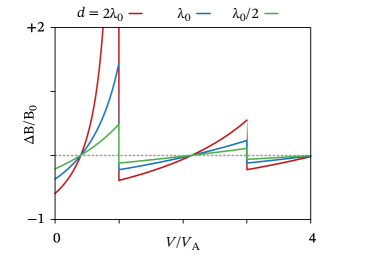
This provides us with a simple analytical result for the linear response of a clean proximitized metal to an applied field . The result is expressed in terms of the Andreev voltage . This can be put into more familiar terms by introducing the superconducting coherence length ; for instance, an N of length would yield . This magnetic shift as function of voltage is shown in Fig. 3.
Discussion.—In the previous sections, we have shown that a paramagnetic Meissner effect can arise in the device in Fig. 1. Moreover, we have shown that whether the response is diamagnetic or paramagnetic can be controlled using a voltage. Our main result is Eq. 15, which provides a simple analytical solution for the magnetic field shift that occurs for a given external magnetic field and voltage . These predictions can be tested using a muon-rotation experiment to directly probe the local magnetic field at different points inside the device, using basically the same setup as in Ref. Di Bernardo et al. (2015).
The striking results are shown in Fig. 3, where we see that for sufficiently thick normal metals, appears to diverge as the voltage approaches the Andreev voltage . Since we considered a completely clean material at zero temperature, there is an abrupt transition between paramagnetism and diamagnetism as the voltage is increased beyond the Andreev voltage. In realistic systems, such sharp features should be smeared out by finite temperature, elastic scattering, and inelastic scattering.
We have also assumed perfect transparency at the S/N interface. Since a finite interface resistance can be expected to dampen the resonance peaks in the DOS of N, we would expect the paramagnetic Meissner effect to become weaker for opaque interfaces. We also note that in regions where , a linear-response calculation is not technically valid anymore, and a full nonlinear-response calculation is warranted if one requires quantitatively rigorous results. Nevertheless, we would expect our results to remain qualitatively valid in such systems, and investigating this rigorously would be an interesting avenue for further research. For instance, whether a paramagnetic instability that generates a spontaneous magnetic flux can appear requires a nonlinear-response calculation Fauchère et al. (1999).
Another interesting proposition for further research, would be to investigate whether a paramagnetic Meissner effect can be induced in dirty systems as well. While no such effect was detected in Ref. Bobkova and Bobkov (2013), they focused on high temperatures and thin superconductors, while the opposite limit may be the relevant one. Even if it is not possible to realize the effect in a dirty S/N structure, the prospect of a voltage-controllable Meissner effect in dirty S/F devices may still be of interest.
Conclusion.—Using a simple linear-response calculation, we have demonstrated how nonequilibrium effects can give rise to a paramagnetic Meissner response. Moreover, we have provided a specific experimental proposal where the magnetic response can be controlled in situ via an applied voltage. In addition to being relevant to the fundamental study of the Meissner effect and odd-frequency superconductivity, our results demonstrate a new way to control the interaction between superconducting structures and magnetic fields via nonequilibrium effects. This paves the way for a new line of research in this direction, and may be relevant to future superconducting device design.
Acknowledgements.
J.A.O. and J.L. were supported by the Research Council of Norway through grant 240806, and its Centres of Excellence funding scheme grant 262633 “QuSpin”. W.B. thanks Arne Brataas and the Centre of Excellence “QuSpin” for hospitality and the DFG through SFB 767 for financial support.References
- Tinkham (2004) M. Tinkham, Introduction to Superconductivity (Dover, 2004).
- Fossheim and Sudbø (2004) K. Fossheim and A. Sudbø, Superconductivity (Wiley, 2004).
- Zaikin (1982) A. Zaikin, Solid State Commun. 41, 533 (1982).
- Belzig et al. (1996) W. Belzig, C. Bruder, and G. Schön, Phys. Rev. B 53, 5727 (1996).
- Müller-Allinger et al. (1999) F. B. Müller-Allinger, A. C. Mota, and W. Belzig, Phys. Rev. B 59, 8887 (1999).
- Belzig et al. (1999) W. Belzig, F. K. Wilhelm, C. Bruder, G. Schön, and A. D. Zaikin, Superlattices and microstructures 25, 1251 (1999).
- Belzig et al. (2007) W. Belzig, C. Bruder, and Y. V. Nazarov, J. Low Temp. Phys. 147, 441 (2007).
- Visani et al. (1990) P. Visani, A. C. Mota, and A. Pollini, Phys. Rev. Lett. 65, 1514 (1990).
- Müller-Allinger and Mota (2000) F. B. Müller-Allinger and A. C. Mota, Phys. Rev. Lett. 84, 3161 (2000).
- Eschrig (2010) M. Eschrig, Physics Today 64, 43 (2010).
- Blamire and Robinson (2014) M. G. Blamire and J. W. A. Robinson, J. Phys. Condens. Matter 26, 453201 (2014).
- Linder and Robinson (2015) J. Linder and J. W. A. Robinson, Nat. Phys. 11, 307 (2015).
- Eschrig (2015) M. Eschrig, Rep. Prog. Phys. 78, 104501 (2015).
- Buzdin (2005) A. I. Buzdin, Rev. Mod. Phys. 77, 935 (2005).
- Bergeret et al. (2005) F. S. Bergeret, A. F. Volkov, and K. B. Efetov, Rev. Mod. Phys. 77, 1321 (2005).
- Berezinskii (1974) V. L. Berezinskii, JETP Lett. 20, 287 (1974).
- (17) J. Linder and A. V. Balatsky, arXiv:1709.03986.
- Bergeret et al. (2001) F. S. Bergeret, A. F. Volkov, and K. B. Efetov, Phys. Rev. B 64, 134506 (2001).
- Yokoyama et al. (2011) T. Yokoyama, Y. Tanaka, and N. Nagaosa, Phys. Rev. Lett. 106, 246601 (2011).
- Asano et al. (2011) Y. Asano, A. A. Golubov, Y. V. Fominov, and Y. Tanaka, Phys. Rev. Lett. 107, 087001 (2011).
- Mironov et al. (2012) S. Mironov, A. Mel’nikov, and A. Buzdin, Phys. Rev. Lett. 109, 237002 (2012).
- Alidoust et al. (2014) M. Alidoust, K. Halterman, and J. Linder, Phys. Rev. B 89, 054508 (2014).
- Espedal et al. (2016) C. Espedal, T. Yokoyama, and J. Linder, Phys. Rev. Lett. 116 (2016).
- Di Bernardo et al. (2015) A. Di Bernardo, Z. Salman, X. L. Wang, M. Amado, M. Egilmez, M. G. Flokstra, A. Suter, S. L. Lee, J. H. Zhao, T. Prokscha, E. Morenzoni, M. G. Blamire, J. Linder, and J. W. A. Robinson, Phys. Rev. X 5 (2015).
- Fauchère et al. (1999) A. L. Fauchère, W. Belzig, and G. Blatter, Phys. Rev. Lett. 82, 3336 (1999).
- Higashitani (1997) S. Higashitani, J. Phys. Soc. Jpn. 66, 2556 (1997).
- Löfwander et al. (2001) T. Löfwander, V. S. Shumeiko, and G. Wendin, Supercond. Sci. Technol. 14, R53 (2001).
- Tanaka et al. (2007) Y. Tanaka, Y. Tanuma, and A. A. Golubov, Phys. Rev. B 76, 054522 (2007).
- Aronov (1973) A. G. Aronov, JETP Lett. 18, 228 (1973).
- Aronov and Spivak (1975) A. G. Aronov and B. Z. Spivak, Sov. Phys. Solid State 17, 1874 (1975).
- Bobkova and Bobkov (2013) I. V. Bobkova and A. M. Bobkov, Phys. Rev. B 88, 174502 (2013).
- Schrieffer (1999) J. R. Schrieffer, Theory of Superconductivity (Perseus, 1999).
- Black and Chandrasekhar (2000) M. J. Black and V. Chandrasekhar, Europhys. Lett. 50, 257 (2000).
- Pothier et al. (1997) H. Pothier, S. Guéron, N. O. Birge, D. Esteve, and M. H. Devoret, Phys. Rev. Lett. 79, 3490 (1997).
- Ouassou et al. (2018) J. A. Ouassou, T. D. Vethaak, and J. Linder, Phys. Rev. B 98, 144509 (2018).
- Keizer et al. (2006) R. S. Keizer, M. G. Flokstra, J. Aarts, and T. M. Klapwijk, Phys. Rev. Lett. 96, 147002 (2006).
- Volkov (1995) A. F. Volkov, Phys. Rev. Lett. 74, 4730 (1995).
- Wilhelm et al. (1998) F. K. Wilhelm, G. Schön, and A. D. Zaikin, Phys. Rev. Lett. 81, 1682 (1998).
- Baselmans et al. (1999) J. J. A. Baselmans, A. F. Morpurgo, B. J. van Wees, and T. M. Klapwijk, Nature 397, 43 (1999).
- Wilhelm et al. (2000) F. K. Wilhelm, G. Schön, and A. D. Zaikin, Physica B 280, 418 (2000).
- Heikkilä et al. (2000) T. T. Heikkilä, F. K. Wilhelm, and G. Schön, Europhys. Lett. 51, 434 (2000).
- Yip (2000) S.-K. Yip, Phys. Rev. B 62, R6127 (2000).
- Chtchelkatchev et al. (2002) N. M. Chtchelkatchev, W. Belzig, and C. Bruder, JETP Lett. 75, 646 (2002).
- Bobkova and Bobkov (2016) I. V. Bobkova and A. M. Bobkov, Phys. Rev. B 93, 024513 (2016).
- (45) J. A. Ouassou and J. Linder, arXiv:1810.02820.
- Snyman and Nazarov (2009) I. Snyman and Y. V. Nazarov, Phys. Rev. B 79, 014510 (2009).
- Moor et al. (2009) A. Moor, A. F. Volkov, and K. B. Efetov, Phys. Rev. B 80, 054516 (2009).
- Chandrasekhar (1962) B. S. Chandrasekhar, Appl. Phys. Lett. 1, 7 (1962).
- Clogston (1962) A. M. Clogston, Phys. Rev. Lett. 9, 266 (1962).
- de Gennes and Saint-James (1963) P. G. de Gennes and D. Saint-James, Phys. Lett. 4, 151 (1963).