Now at ]Research and Prototype Foundry, The University of Sydney, NSW 2006, Australia.
Silicon quantum processor unit cell operation above one Kelvin
Quantum computers are expected to outperform conventional computers for a range of important problems, from molecular simulation to search algorithms, once they can be scaled up to large numbers of quantum bits (qubits), typically millions Feynman1982 ; Loss1998 ; Fowler2012 . For most solid-state qubit technologies, e.g. those using superconducting circuits or semiconductor spins, scaling poses a significant challenge as every additional qubit increases the heat generated, while the cooling power of dilution refrigerators is severely limited at their operating temperature below 100 mK Devoret2004 ; Vandersypen2017 ; Almudever2017 . Here we demonstrate operation of a scalable silicon quantum processor unit cell, comprising two qubits confined to quantum dots (QDs) at 1.5 Kelvin. We achieve this by isolating the QDs from the electron reservoir, initialising and reading the qubits solely via tunnelling of electrons between the two QDs Bertrand2015 ; Veldhorst2017 ; Crippa2018 . We coherently control the qubits using electrically-driven spin resonance (EDSR) Pioro2008 ; Leon2019 in isotopically enriched silicon 28Si itoh_watanabe_2014 , attaining single-qubit gate fidelities of 98.6% and coherence time = 2 s during ‘hot’ operation, comparable to those of spin qubits in natural silicon at millikelvin temperatures Takeda2016 ; Kawakami2016 ; Watson2018 ; Zajac2018 . Furthermore, we show that the unit cell can be operated at magnetic fields as low as 0.1 T, corresponding to a qubit control frequency of 3.5 GHz, where the qubit energy is well below the thermal energy. The unit cell constitutes the core building block of a full-scale silicon quantum computer, and satisfies layout constraints required by error correction architectures Veldhorst2017 ; Jones2018 . Our work indicates that a spin-based quantum computer could be operated at elevated temperatures in a simple pumped 4He system, offering orders of magnitude higher cooling power than dilution refrigerators, potentially enabling classical control electronics to be integrated with the qubit array Hornibrook2015 ; Degenhardt2017 .
Electrostatically gated QDs in Si/SiGe or Si/SiO2 heterostructures are prime candidates for spin-based quantum computing due to their long coherence times, high control fidelities, and industrial manufacturability Veldhorst2014 ; Kawakami2016 ; Marurand2016 ; Takeda2016 ; Yoneda2018 ; Yang2019 . In large scale quantum processors the qubits will be arranged in either 1D chains Jones2018 or 2D arrays Fowler2012 to enable quantum error correction schemes. For architectures relying on exchange coupling for two-qubit operation Veldhorst2015 ; Watson2018 ; Zajac2018 ; Huang2018 , the QDs are expected to be densely packed. Until now, two-qubit QD systems have been tunnel-coupled to a nearby charge reservoir that has typically been used for initialisation and readout using spin-to-charge conversion Elzerman2004 . Here we demonstrate an isolated double QD system that requires no tunnel-coupled reservoir Bertrand2015 ; Veldhorst2017 ; Crippa2018 to perform full two-qubit initialisation, control and readout – thus realising the elementary unit cell of a scalable quantum processor (see Figure 1h).

Figure 1a shows a scanning electron microscope (SEM) image of a silicon metal-oxide-semiconductor (Si-MOS) double QD device nominally identical to the one measured. The device is designed with a cobalt micromagnet to facilitate EDSR, whereby an AC voltage at frequency is applied to the micromagnet electrode to drive spin resonance Pioro2008 , and a single electron transistor (SET) charge sensor is used to detect changes in the electron occupation of the two QDs Leon2019 . The experimental setup is described in 1. In Figure 1b-f we illustrate the tuning sequence that we use to configure the isolated double QD unit cell in the (3,3) charge configuration. We start by accumulating the desired total number of electrons under G1, then deplete the electrons under gate J and G2, and finally cut off the electron reservoir by lowering the bias applied to the barrier gate B. At the end of the tuning sequence, the strong barrier confinement ensures no electrons can tunnel into or out of the qubit cell. The ability to operate the unit cell without any changes in electron occupation throughout initialization, control and readout is the prerequisite for scaling it up to large 2D arrays (see Figure 1h), where qubit control can be achieved by global magnetic resonance or via an array of micromagnets that allow local EDSR. Using the gates G1, J and G2 (see Figure 1g) we can distribute the 6 electrons arbitrarily within the qubit cell, as demonstrated in the stability diagram shown in Figure 1i. In this work, we focus on the (3,3) charge configuration (See 2). Here, the lower two electrons in each dot form a spin-zero closed shell in the lower conduction-band valley state, and we use the spins of the unpaired electrons in the upper valley states of the silicon QDs as our qubits Veldhorst2015b . It is also possible to operate the qubits in the (1,1) and (1,3) charge configurations (see 3), but (3,3) is chosen for better EDSR driving strength and J-gate control Leon2019 .

We depict the entire control, measurement and initialisation cycle in Figure 2a,b. Throughout operation, the same six electrons stay within the unit cell. We measure the two-spin state based on a variation of the Pauli spin blockade. As for traditional singlet-triplet readout Ono2002 , tunnelling of the electrons into the same dot is only allowed for a spin singlet state due to the Pauli exclusion principle. On the other hand, not all triplets are blockaded – the triplet mixes with the singlet state at a rate faster than our SET charge readout. Therefore any combination of and will be allowed to tunnel. As a result, spin-to-charge conversion in our device manifests itself as spin parity readout, measuring the projection of the two-qubit system, where is the Pauli operator (see Methods).
In the remainder of the paper, we denote this parity readout output as , the expectation value of . An even spin state readout then leads to and an odd state leads to .
Initialisation is based on first preparing the unit cell in the (2,4) state, before moving one electron to Qubit 1 (Q1) to create a (3,3) -like state. For we can also initialise the system in the well-defined state by dwelling at a spin relaxation hot-spot Watson2018 ; Huang2018 . In Figure 2c we show Rabi oscillations for the two different initialisation states, starting in either the -like or the state. Additional verification of the initialised states is performed by spin relaxation measurements described in Methods section and 4.
We confirm that our readout procedure distinguishes the state parity by serially driven Rabi rotations shown in Figure 2d, where we coherently and unconditionally rotate first Q1 and then Q2, and measure the output state. Reading other two-qubit projections is also straightforward. Rotating one of the qubits by we gain access to , where . Furthermore, adding a conditional two-qubit gate like a CNOT before readout, we can turn the parity readout into a single qubit readout. Figure 2e shows the pulse sequence from Figure 2d with an added CNOT gate based on performing a conditional-Z (CZ) gate. We achieve the conditional phase shift by pulsing the J gate to temporarily increase the coupling between the two qubits (without changing the charge detuning). The single qubit readout result is shown in Figure 2f. The sequence reads out only the Q1 spin state as , independent of Q2. To read out Q2, one would simply need to swap target and control of the CNOT gate. The small but visible oscillations along the -axis in the data are due to imperfect CZ pulsing. Details of the CNOT gate data are shown in 5, where the CNOT gate parameters in panel c are the same as those for Figure 2f.
Having demonstrated the general operation of the quantum processor unit cell including initialisation, one- and two-qubit control, and parity and single-qubit readout, we can now investigate the effect of temperature. For large scale quantum computer integration, the benefits of raising the temperature to reduce engineering constraints have to be carefully balanced with the presence of increased noise. Prior studies have examined the relaxation of Si-MOS QD spin qubits at temperatures of 1.1 K Petit2018 and coherence times of ensembles of Si-MOS QDs up to 10 K Shankar2010 . The coherence times of single deep-level impurities in silicon at 10 K Ono2019 and ensembles of donor electron spins in silicon up to 20 K Tyryshkin2003 ; Tyryshkin2012 were also examined. However, coherence times and gate fidelities of these qubits have not been investigated as yet. Here we investigate the gate fidelity of a fully-controllable spin qubit at 1.5 Kelvin.
In Figure 3 we present single-qubit Rabi chevrons and randomised benchmarking for temperatures of mK in Figure 3a-d, and K in Figure 3e-h. Here, K is achieved by simply pumping on the 4He in the 1K pot of the dilution refrigerator, while the 3He circulation is completely shut off. Qubit operation and readout at this elevated temperature is possible since our QDs have relatively high valley splitting ( eV) and orbital splitting energies ( meV) Leon2019 . We observe Rabi chevrons, indicating coherent qubit control, for both T and T at K, despite the thermal energy being larger than the qubit energy ().
From the decay of the Ramsey oscillations in Figure 3g we determine a coherence time at this elevated temperature of s, comparable to that in natural silicon at mK temperatures Takeda2016 ; Kawakami2016 ; Watson2018 ; Zajac2018 . The single qubit gate fidelity extracted from randomised benchmarking is %, nearly at the fault tolerant level (see Figure 3h). For reference, the qubit’s performance at mK is shown in Figure 3a-d, at which both and are about 6 times better.
We present a more detailed study of the coherence times and relaxation times as a function of mixing chamber temperature in Figure 4. A similar study as a function of external magnetic field is presented in 8, where we observe the Hahn echo time to scale linearly with , where shorter relaxation times at lower field are possibly due to spin-orbit Johnson noise struck2019spin . Temperature has the strongest impact on , which scales as between 0.5 and 1.0 K. This could be interpreted as a Raman process involving intervalley piezophonons stemming from the oxide layer – if the spin-lattice relaxation was dominated by Si deformation potential phonons, the temperature power law should be stronger, as discussed in Ref. Petit2018 . and display a weaker dependence on temperature.
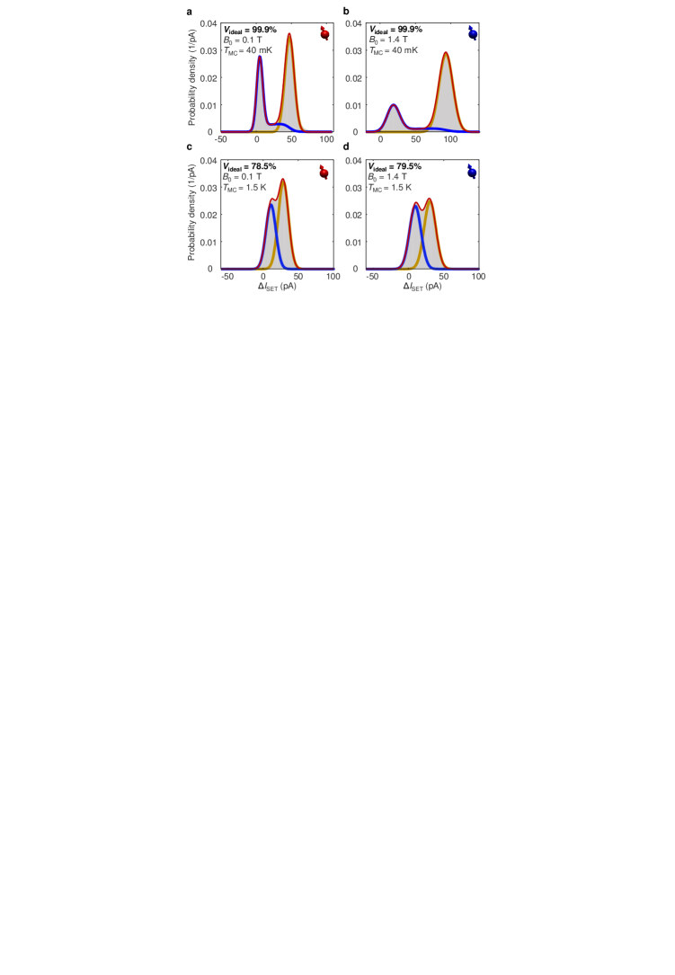
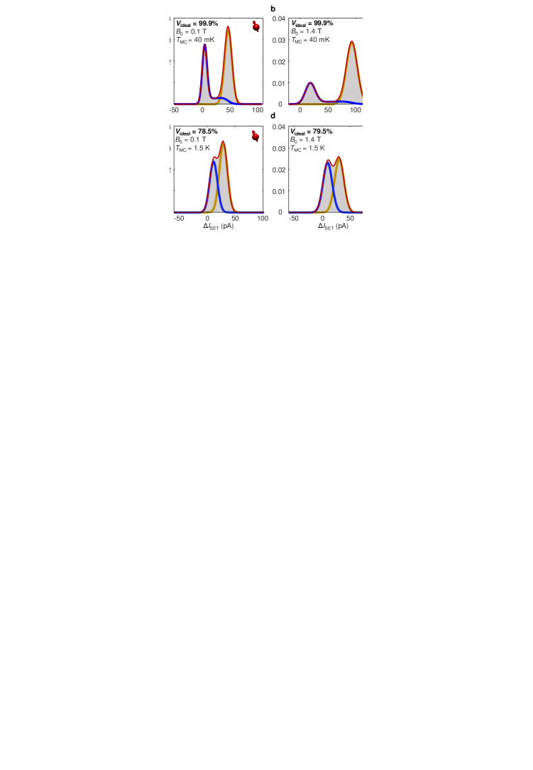
The results in Figure 4 show a significant reduction in spin relaxation and coherence times going from 100 mK to 1.5 K. While this reduction does not prevent the qubits from being operated at this temperature, future device engineering should aim to minimise possible sources of noise for optimised high-temperature operation. Residual 29Si nuclear spins that couple to the qubits through the hyperfine interaction lead to background magnetic field noise that could be easily reduced by using silicon substrates with higher isotopic enrichment Witzel2010 . Our devices contain ppm residual 29Si atoms, which is more than one order of magnitude higher than what is currently available Tyryshkin2012 ; itoh_watanabe_2014 . While the gradient magnetic field from a micromagnet, as required for EDSR operation Pioro2008 ; Kawakami2016 ; Leon2019 , might freeze out nuclear spin dynamics Tyryshkin2012 , it will also make the qubits more sensitive to electric field noise induced by the artificial spin-orbit coupling struck2019spin . Charge noise has been shown to increase with temperature Petit2018 , and could constitute the dominant noise source for EDSR systems at elevated temperatures. Furthermore, since the drop in visibility in Figure 3 can be attributed to a lower charge readout fidelity owing to the broadening of the SET peak (see 9), replacing SET current readout with a readout mechanism that offers better signal to noise ratios should improve readout fidelities at higher temperatures. Radio-frequency gate dispersive readout West2019 ; Crippa2018 could act as a solution, while, at the same time, providing a truly scalable unit cell footprint.
In conclusion, we have presented a fully operable two-qubit system in an isolated quantum processor unit cell, which allows operation up to 1.5 K – a temperature that is conveniently achieved using pumped 4He cryostats – where we reach near fault-tolerant single-qubit fidelities. These results pave the way for scaling of silicon-based quantum processors to very large numbers of qubits.
References
- (1) Feynman, R. P. Simulating physics with computers. International Journal of Theoretical Physics 21, 467–488 (1982). URL https://doi.org/10.1007/BF02650179.
- (2) Loss, D. & DiVincenzo, D. P. Quantum computation with quantum dots. Physical Review A 57, 120 (1998). URL https://doi.org/10.1103/PhysRevA.57.120.
- (3) Fowler, A. G., Mariantoni, M., Martinis, J. M. & Cleland, A. N. Surface codes: Towards practical large-scale quantum computation. Physical Review A 86, 032324 (2012). URL https://doi.org/10.1103/PhysRevA.86.032324.
- (4) Devoret, M. H., Wallraff, A. & Martinis, J. M. Superconducting qubits: A short review. arXiv:0411174 (2004). URL https://arxiv.org/abs/cond-mat/0411174.
- (5) Vandersypen, L. et al. Interfacing spin qubits in quantum dots and donors—hot, dense, and coherent. npj Quantum Information 3, 34 (2017). URL https://doi.org/10.1038/s41534-017-0038-y.
- (6) Almudever, C. G. et al. The engineering challenges in quantum computing. In 2017 Design, Automation & Test in Europe Conference & Exhibition (DATE), 836–845 (IEEE, 2017). URL https://doi.org/10.23919/DATE.2017.7927104.
- (7) Bertrand, B. et al. Quantum manipulation of two-electron spin states in isolated double quantum dots. Phys. Rev. Lett. 115, 096801 (2015). URL https://doi.org/10.1103/PhysRevLett.115.096801.
- (8) Veldhorst, M., Eenink, H. G. J., Yang, C. H. & Dzurak, A. S. Silicon CMOS architecture for a spin-based quantum computer. Nature Communications 8, 1766 (2017). URL https://doi.org/10.1038/s41467-017-01905-6.
- (9) Crippa, A. et al. Gate-reflectometry dispersive readout of a spin qubit in silicon. arXiv:1811.04414 (2018). URL https://arxiv.org/abs/1811.04414.
- (10) Pioro-Ladrière, M. et al. Electrically driven single-electron spin resonance in a slanting Zeeman field. Nature Physics 4, 776 (2008). URL https://doi.org/10.1038/nphys1053.
- (11) Leon, R. C. C. et al. Coherent spin control of s-, p-, d- and f-electrons in a silicon quantum dot. arXiv:1902.01550 (2019). URL https://arxiv.org/abs/1902.01550.
- (12) Itoh, K. M. & Watanabe, H. Isotope engineering of silicon and diamond for quantum computing and sensing applications. MRS Communications 4, 143–157 (2014). URL https://doi.org/10.1557/mrc.2014.32.
- (13) Takeda, K. et al. A fault-tolerant addressable spin qubit in a natural silicon quantum dot. Science Advances 2, e1600694 (2016). URL https://doi.org/10.1126/sciadv.1600694.
- (14) Kawakami, E. et al. Gate fidelity and coherence of an electron spin in an Si/SiGe quantum dot with micromagnet. Proceedings of the National Academy of Sciences 113, 11738–11743 (2016). URL https://doi.org/10.1073/pnas.1603251113.
- (15) Watson, T. F. et al. A programmable two-qubit quantum processor in silicon. Nature 555, 633 (2018). URL https://doi.org/10.1038/nature25766.
- (16) Zajac, D. M. et al. Resonantly driven CNOT gate for electron spins. Science 359, 439–442 (2018). URL https://doi.org/10.1126/science.aao5965.
- (17) Jones, C. et al. Logical qubit in a linear array of semiconductor quantum dots. Physical Review X 8, 021058 (2018). URL https://doi.org/10.1103/PhysRevX.8.021058.
- (18) Hornibrook, J. M. et al. Cryogenic control architecture for large-scale quantum computing. Phys. Rev. Applied 3, 024010 (2015). URL https://doi.org/10.1103/PhysRevApplied.3.024010.
- (19) Degenhardt, C., Geck, L., Kruth, A., Vliex, P. & van Waasen, S. CMOS based scalable cryogenic control electronics for qubits. In Rebooting Computing (ICRC), 2017 IEEE International Conference on, 1–4 (IEEE, 2017). URL https://doi.org/10.1109/ICRC.2017.8123682.
- (20) Veldhorst, M. et al. An addressable quantum dot qubit with fault-tolerant control-fidelity. Nature Nanotechnology 9, 981–985 (2014). URL https://doi.org/10.1038/Nnano.2014.216.
- (21) Maurand, R. et al. A CMOS silicon spin qubit. Nature Communications 7, 13575 (2016). URL https://doi.org/10.1038/ncomms13575.
- (22) Yoneda, J. et al. A quantum-dot spin qubit with coherence limited by charge noise and fidelity higher than 99.9%. Nature Nanotechnology 13, 102–106 (2018). URL https://doi.org/10.1038/s41565-017-0014-x.
- (23) Yang, C. H. et al. Silicon qubit fidelities approaching incoherent noise limits via pulse engineering. Nature Electronics 2, 151–158 (2019). URL https://doi.org/10.1038/s41928-019-0234-1.
- (24) Veldhorst, M. et al. A two-qubit logic gate in silicon. Nature 526, 410 (2015). URL https://doi.org/10.1038/nature15263.
- (25) Huang, W. et al. Fidelity benchmarks for two-qubit gates in silicon. Nature 569, 532–536 (2019). URL https://doi.org/10.1038/s41586-019-1197-0.
- (26) Elzerman, J. M. et al. Single-shot read-out of an individual electron spin in a quantum dot. Nature 430, 431 (2004). URL https://doi.org/10.1038/nature02693.
- (27) Veldhorst, M. et al. Spin-orbit coupling and operation of multivalley spin qubits. Phys. Rev. B 92, 201401 (2015). URL https://doi.org/10.1103/PhysRevB.92.201401.
- (28) Ono, K., Austing, D., Tokura, Y. & Tarucha, S. Current rectification by Pauli exclusion in a weakly coupled double quantum dot system. Science 297, 1313–1317 (2002). URL https://doi.org/10.1126/science.1070958.
- (29) Petit, L. et al. Spin lifetime and charge noise in hot silicon quantum dot qubits. Physical Review Letters 121, 076801 (2018). URL https://doi.org/10.1103/PhysRevLett.121.076801.
- (30) Shankar, S., Tyryshkin, A. M., He, J. & Lyon, S. A. Spin relaxation and coherence times for electrons at the Si/SiO2 interface. Phys. Rev. B 82, 195323 (2010). URL https://doi.org/10.1103/PhysRevB.82.195323.
- (31) Ono, K., Mori, T. & Moriyama, S. High-temperature operation of a silicon qubit. Scientific Reports 9, 469 (2019). URL https://doi.org/10.1038/s41598-018-36476-z.
- (32) Tyryshkin, A. M., Lyon, S. A., Astashkin, A. V. & Raitsimring, A. M. Electron spin relaxation times of phosphorus donors in silicon. Phys. Rev. B 68, 193207 (2003). URL https://doi.org/10.1103/PhysRevB.68.193207.
- (33) Tyryshkin, A. M. et al. Electron spin coherence exceeding seconds in high-purity silicon. Nature Materials 11, 143 (2012). URL https://doi.org/10.1038/nmat3182.
- (34) Struck, T. et al. Spin relaxation and dephasing in a 28SiGe QD with nanomagnet. Bulletin of the American Physical Society (2019). URL https://meetings.aps.org/Meeting/MAR19/Session/B35.9.
- (35) Witzel, W. M., Carroll, M. S., Morello, A., Cywiński, Ł. & Sarma, S. D. Electron spin decoherence in isotope-enriched silicon. Physical Review Letters 105, 187602 (2010). URL https://doi.org/10.1103/PhysRevLett.105.187602.
- (36) West, A. et al. Gate-based single-shot readout of spins in silicon. Nature Nanotechnology 14, 437–441 (2019). URL https://doi.org/10.1038/s41565-019-0400-7.
- (37) Angus, S. J., Ferguson, A. J., Dzurak, A. S. & Clark, R. G. Gate-defined quantum dots in intrinsic silicon. Nano Letters 7, 2051–2055 (2007). URL https://doi.org/10.1021/nl070949k.
- (38) Lim, W. H. et al. Observation of the single-electron regime in a highly tunable silicon quantum dot. Applied Physics Letters 95, 242102 (2009). URL https://doi.org/10.1063/1.3272858.
- (39) Medford, J. et al. Self-consistent measurement and state tomography of an exchange-only spin qubit. Nature Nanotechnology 8, 654 (2013). URL https://doi.org/10.1038/nnano.2013.168.
Methods
Feedback controls
Three types of feedback/calibration processes are implemented for the experiments:
-
•
SET sensor current feedback – For each current trace acquired by the digitizer, during the Reset stage is compared against a set value. In case of Figure 2a this set value is 50 pA. The SET top-gate voltage is then adjusted to ensure stays at 50 pA.
-
•
Charge detuning feedback – The charge detuning level between the two dots is controlled by monitoring the bias at which the charge transition occurs, shown by the red arrow in Figure 2a. Adjusting the bias on , the charge transition is then retuned to occur at 60% of the Read Feedback stage.
- •
Temperature control
For operation at base temperature , the circulation of 3He is fully enabled. For and , we turn on the heater at the mixing chamber stage (See 1) with a Proportional Integral (PI) computer controller. For , the 3He circulation is completely stopped by closing the circulation valves, and turning off all heaters. The fridge is then left for at least 1 day for to saturate at 1.5 K, the temperature of the 1K pot stage. The 1K pot was actively pumped during all the measurements in this work.
To validate the temperature accuracy, we performed effective electron temperature measurements of the isolated QDs by measuring the broadening of the (2,4)-(3,3) charge transition as shown in 6a. Having determined the lever arms from magnetospectroscopy (see 7) we fit the charge transitions to extract the effective electron temperatures (see 6b). For K, the extracted temperature matches well with the mixing chamber thermometer of the fridge.
Wait-time-dependent phase Ramsey measurement
To extract times at high temperatures, where the control pulses are of similar duration as the coherence time, the conventional way of setting a resonance frequency detuning would greatly suppress the already low visibility of the oscillations. A more efficient way to extract is to use zero-detuning pulses while applying a large wait-time-dependent phase shift to the second -pulse. This results in fast Ramsey fringes while maintaining maximum visibility. For example, in Figure 3g, the phase of the second microwave pulse has the dependency , giving Ramsey fringes with a frequency of 2 MHz.
For all Ramsey measurements, each data point consist of 100 single shots per acquisition, with 5 overall repeats, giving a total of 500 single shots.
Parity readout
In general, the joint state of a pair of spins may be measured through a spin-to-charge conversion based on the Pauli exclusion principle. In a double dot system, interdot tunnelling is stimulated by detuning the energy levels of one quantum dot with respect to the other. If the pair of electrons is in the singlet state, tunnelling will occur and the charge distribution in the double dot will change. A charge measurement then allows us to distinguish a singlet state from any one of the spin triplets.
For simplicity, we will refer to the possible charge configurations as , but any configuration with two effective valence spins is valid, including the (3,3) charge configuration investigated in this work. If Pauli spin blockade occurred in the standard way, we would have the simple mapping
| (1) | |||||
| (2) | |||||
| (3) | |||||
| (4) |
and the final state after the measurement would be a pure state. A measurement of the charge state would distinguish singlets from triplets, i.e., discern between distinct eigenstates of total angular momentum .
In practice, relaxation between the triplet states and the singlet ground state occurs at the same time as the charge measurement process. Spin flip relaxation is slower than 10 ms for all temperatures studied here, as shown in Figure 4 of the main text, so that the and states will be preserved for a sufficiently long time for our SET-based measurement to be completed.
On the other hand, the triplet and the singlet are constantly mixing with each other, either through the difference in Overhauser fields from nuclear spins (reduced here in isotopically enriched 28Si), difference in g-factors under external applied magnetic field, or due to the micromagnet field gradient.
The wavefunction component of that mixes into the state rapidly relaxes into the state. This means that at the time scale of the mixing, the population in is depleted and relaxes into .
Since this relaxation mechanism is much faster than any spin flip mechanism, after a sufficiently long time (compared to the mixing rate and the tunnel/charge relaxation rate), the state has completely relaxed into the singlet state and the mapping connects again two pure states
| (5) | |||||
| (6) | |||||
| (7) | |||||
| (8) |
Now, a charge measurement can distinguish between states of parallel spin state or anti-parallel spins, represented by the observable . This measurement therefore corresponds to a parity read-out.
.1 Confirming initialisations using spin relaxation
By preparing a state we measure the spin relaxation time for both qubits by selectively flipping one of them to a spin up state, followed by a wait time, . 4a-c are fitted using a simple decay equation , when driving a, Q1 to spin up, b, off-resonance drive, and c, Q2 to spin up. The two qubits have = 540 ms and 36 ms, respectively.
When we repeat the same measurement with a -like initialisation, we observe a mixed decay pattern. We now need to fit to a more complicated equation that measures the parity of the spins while both spins are relaxing, assuming no knowledge of the initial state.
For and components, the relaxation equations for parity readout are:
| (9) | |||
| (10) |
where
| (11) | |||
| (12) |
For a component, assuming no two-spin interactions, it is then:
| (13) |
Combining the three equations above, for an arbitrary initial state fitting we obtain:
| (14) |
Equation 14 is then applied to fit 4d-f, which then gives the probability of each eigenstate for -like initialisation, proving indeed it is an equal mixture of and states.
Acknowledgements
We acknowledge support from the US Army Research Office (W911NF-17-1-0198), the Australian Research Council (CE170100012), Silicon Quantum Computing Proprietary Limited, and the NSW Node of the Australian National Fabrication Facility. The views and conclusions contained in this document are those of the authors and should not be interpreted as representing the official policies, either expressed or implied, of the Army Research Office or the U.S. Government. The U.S. Government is authorised to reproduce and distribute reprints for Government purposes notwithstanding any copyright notation herein. K. M. I. acknowledges support from Grant-in-Aid for Scientific Research by MEXT. J. C. L. and M. P.-L. acknowledge support from the Canada First Research Excellence Fund and in part by the National Science Engineering Research Council of Canada. K. Y. T. acknowledges support from the Academy of Finland through project Nos. 308161, 314302 and 316551.
Author contributions
C.H.Y designed and performed the experiments. C.H.Y., R.C.C.L. and A.S analysed the data. J.C.C.H. and F.E.H. fabricated the device with A.S.D’s supervision. J.C.C.H., T.T. and W.H contributed to the preparation of experiments. J.C.L., R.C.C.L., J.C.C.H., C.H.Y. and M.P.-L. designed the device. K.W.C., K.Y.T. contributed to discussions on the nanofabrication process. K.M.I. prepared and supplied the 28Si epilayer. T.T., W.H., A.M. and A.L. contributed to results discussion and interpretation. C.H.Y., A.S., A.L. and A.S.D. wrote the manuscript with input from all co-authors.
![[Uncaptioned image]](/html/1902.09126/assets/x5.png)
![[Uncaptioned image]](/html/1902.09126/assets/x6.png)
![[Uncaptioned image]](/html/1902.09126/assets/x7.png)
![[Uncaptioned image]](/html/1902.09126/assets/x8.png)
![[Uncaptioned image]](/html/1902.09126/assets/x9.png)
![[Uncaptioned image]](/html/1902.09126/assets/x10.png)
![[Uncaptioned image]](/html/1902.09126/assets/x11.png)
![[Uncaptioned image]](/html/1902.09126/assets/x12.png)
![[Uncaptioned image]](/html/1902.09126/assets/x13.png)