Theory of optically induced Förster Coupling in van der Waals coupled Heterostuctures
Abstract
We investigate the impact of optically induced Förster coupling in van der Waals heterostructures consisting of graphene and a monolayer transition metal dichalcogenide (TMD). In particular, we predict the corresponding dephasing rates and a fast energy transfer between the TMD layer and graphene being in the picosecond range. Exemplary we find a transition rate of thermalized excitons of about 4 ps-1 in a MoSe2-graphene stack at room temperature. This timescale is in good agreement with the recently measured exciton lifetime in this heterostructure.
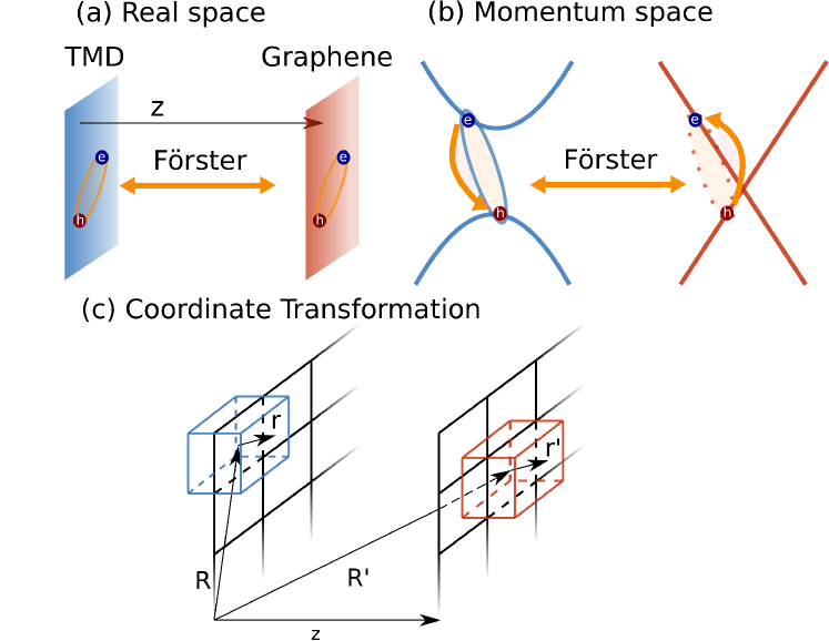
Since the discovery of graphene in 2004, a new research field on atomically thin quasi two dimensional (2D) materials has been established. In particular, monolayers of transition metal dichalcogenides (TMDs) became one of the most investigated materials beyond graphene. They exhibit technologically promising characteristics, such as a direct band gap, tightly bound electron-hole pairs (excitons)Mak et al. (2010); Ramasubramaniam (2012); Chernikov et al. (2014), strong light-matter interactionLi et al. (2014); Moody et al. (2015), and valley-selective circular dichroism Cao et al. (2012); Schmidt et al. (2016). Recent progress in growth techniques has also enabled the production of van der Waals heterostructures by vertically stacking atomically thin monolayers Shi et al. (2012); Geim and Grigorieva (2013). Consequently, heterostructures consisting of graphene and a monolayer TMD have been investigated theoretically Trushin (2018) and experimentally Georgiou et al. (2012); Britnell et al. (2013); He et al. (2014); Lin et al. (2014); Zhang et al. (2014); Hill et al. (2017); Froehlicher et al. (2018). Performing differential reflection measurements, J. He and co-workers found the relaxation of optically injected carriers from tungsten disulfide to graphene to occur within 1 psHe et al. (2014). In recent photoluminescence measurements G. Froelicher and co-workers found found a shortened exciton lifetime of about 1 ps in a coupled MoSe2-graphene structure at room temperature Froehlicher et al. (2018). In another study, Hill and co-workers found an additional broadening of 5 meV and a redshift of 23 meV of the excitonic resonance in a linear optics experiment due to the coupling between monolayer WS2 and grapheneHill et al. (2017). The experimental data have not been complemented by microscopic theory yet: Possible coupling mechanisms constitute of electronic tunneling, Dexter- and Förster energy transfer Richter et al. (2006); Rozbicki and Machnikowski (2008); Specht et al. (2015); Ovesen et al. (2018). Since both materials exhibit strong optical dipole moments, Förster coupling is expected to have a significant impact on the excitation transfer in these heterostructures, if the barrier potential is large enough to suppress electronic overlap Specht et al. (2015), cf. Fig. 1.
Förster-induced relaxation dynamics were investigated recently in heterostructures of different dimensions, namely between quantum dotsRichter et al. (2006); Rozbicki and Machnikowski (2008), between graphene and attached moleculesMalic et al. (2014) and between two quantum wellsBatsch et al. (1993). Here, we present a microscopic approach based on the Heisenberg equation of motion formalism allowing us to derive an analytic description of the Förster coupling in a van der Waals heterostructure consisting of graphene and a TMD monolayer. We predict the impact of the Förster coupling on the optical response of the heterostructure including the linewidth and spectral shift of excitonic resonances. In principle, also charge transfer (tunneling and Dexter processes) between both monolayers could affect the spectral width and the spectral position of the exciton line in the TMD monolayer. However, charge transfer does strongly dependent on the overlap of the wavefunctions of electrons in the TMD and graphene. For electronically decoupled monolayers, the Förster coupling can be expected to dominate tunnel and Dexter coupling Specht et al. (2015). For closely stacked heterostuctures however further investigation are required to evaluate the actual strength of the Dexter- and tunnel- coupling. This requires first principle methods and is addressed in future work. On the other hand, pure Förster coupling provides at least a limiting case that can be discussed in the analysis of experiments without or involving electronic overlap.
I Theoretical Model
We start with defining the many-particle Hamilton operator describing the Coulomb interaction between an exemplary TMD layer and graphene
| (1) |
with electron annihilation (creation) operators acting on states with the band index and the momentum . We denote electrons in the TMD monolayer by and in graphene by . The appearing Coulomb matrix element inducing the Förster transfer reads
| (2) |
with the single particle electronic wavefunctions . We consider both materials to be aligned in the x-y-plane. Further, denotes the three dimensional Coulomb potential, with the vacuum permittivity and the mean dielectric constant of the surrounding material. This assumption is valid, since it differs only weakly from the exact static Coulomb potential for a dielectric surrounding typically found in experiments Hill et al. (2017), i.e. a TMD monlayer on a quartz substrate. This was checked carefully by explicitly evaluating the Possion equation Ovesen et al. (2018). Next, we decompose the space coordinates in both constituents in pointing to the center of the n-th unit cell (uc) and describing a point within the unit cell. Thus, the integral transforms to . Here, the sum over the unit cells is restricted to the monolayers, whereas the integrations are performed in the 3 dimensional unit cells, cf. figure 1 (c). Now, we perform a Taylor expansion for the intra cell coordinate and assume which can only be fulfilled, if the wavefunctions of the electrons in graphene and the TMD layer do not overlap. Here, denotes the distance between both constituents. The monopole-monopole contribution of the Taylor expansion can be shown to contribute to the diagonal part of the Hamiltonian, providing an energy renormalization with respect to the uncoupled TMD-graphene heterostructure Richter et al. (2006). This energy renormalization vanishes in the linear optics limit and is therefore neglected in the following. The monopole-dipole can be neglected within the rotating-wave approximation of excitation with optical frequencies Specht et al. (2015) and therefore the dominating part is the dipole-dipole contribution of the Coulomb potential
Assuming electronic Bloch functions in both structures, we obtain for the coupling element
| (3) |
denotes the dipole moment with the lattice-periodic Bloch factor and the area of the unit cell . The Bloch factors further contain envelope functions ensuring the confinement in -direction. Since they are normalized with respect to the -integration, they drop in the computation.
To further evaluate the sums over , we introduce center-of-mass coordinates and , with being the vector pointing from the TMD layer to the graphene layer. Then, we obtain the matrix element:
| (4) | |||
Without loss of generality, we write the dipole moments as and with denoting the directions of the dipole moments in the TMD layer and in graphene, respectively. Before we provide the final Hamiltonian for the Förster coupling, we evaluate the sums over the electronic bands. We find, that contributions with and do not induce an interlayer energy transfer but an energy renormalization Specht et al. (2015). This renormalization vanishes in the limit of linear optics and therefore is dropped from the Hamiltonian. Additionally we perform a rotating frame approximation to remove non-energy conserving terms for excitations with optical frequencies from the Hamiltonian. Thus we obtain the Hamiltonian
| (5) |
with
The next step is to introduce electron-hole pair polarizations in the TMD and in graphene to further simplify the Hamilton operator. Performing a transformation to center-of-mass coordinates and projecting the relative coordinate to exciton wavefunctions in graphene and in the TMD layer with quantum numbers and , we obtain for the Hamiltonian
| (6) |
Now, we assume that the dipole moments do not depend on the momentum at the band minimum ( and ) and exploit the fact that at optical frequencies there are no bound excitons in graphene, thus we approximate in the free particle limit. In contrast, for TMDs with strongly bound excitons, we use the relation (where is the TMD exciton wavefunction in realspace). The TMD wavefunction is obtained as eigenvector of the Wannier equation Haug and Koch ; Berghäuser and Malic (2014), where we treated the appearing Coulomb potential within the Keldysh approach to account for the finite width of the TMD monolayerKeldysh (1978); Berkelbach et al. (2013). We obtain the Förster coupling Hamilton operator
| (7) |
with the center of mass dependent Förster coupling element . The Förster Hamiltonian, eq. 7, can be interpreted as the annihilation of a bound exciton in the TMD monolayer and the creation of a free electron hole pair in the graphene monolayer, cf. figure 1 (b).
Now, we have all ingredients to define the Bloch equations for the exciton polarizations by exploiting the Heisenberg equation of motion
| (8) | ||||
| (9) |
The first term in both equations accounts for the free energy of the polarizations with being the spectral position of the TMD exciton and as the total mass of the exciton. In graphene, we assume the energy to be independent of the center-of-mass momentum with as the Fermi velocity, since typically it holds and the dispersion of graphene is linear in the investigated -region for coherent or even thermalized TMD excitons. The remaining terms in eqs. (8) and (9) result from the Förster coupling between both monolayers. The coupled eqs. (8) and (9) describe new quasiparticles from electron-hole pairs in graphene and excitons in TMDs. The most direct approach in the weak coupling limit is to perform a Born-Markov approximationKuhn and Rossi (1992); Schilp et al. (1994); Scully and Zubairy (1997) for the polarization in graphene . This approximation is valid as long as the Förster induced interlayer coupling is small compared to the spectral bandwidth provided by the broad electronic energy distribution in graphene. The Born Markov approximation carried out is formally equivalent to a Wigner-Weisskopf approximation where the graphene continuum acts as a bathScully and Zubairy (1997). This way, we have access to the dephasing rate and the energy renormalization for excitons in the TMD due to Förster coupling with the graphene layer:
| (10) |
For the broadening we obtain
| (11) | |||
| (12) |
while the energy renormalization reads
| (13) | ||||
| (14) |
Here, we neglect the Förster interaction mediated influence of different TMD excitons on each other. For an optical excitation, we have , where is the incident laser frequency. Note that we added a factor of to take account to the spin degree of freedom in graphene. Note that the momentum sum appearing in the expression for the lineshift, equation 13, in general diverges. This problem is also known from the computation of the Lambshift, where the atomic states couple to the mode continuum of the radiational field which results in a divergent self energy contributionScully and Zubairy (1997). Similar, in the current case, the energy renormalization does depend on the choice of a physically motivated momentum cutoff . Therefore we do not compute the energy renormalization explicitly but will discuss it qualitatively in the following. We find that the dephasing rate, eq. (12), and the energy renormalization, eq. (14), show the same momentum and layer separation dependence, since both are proportional to .
The appearing function in eqs. 12 and 14 has to be evaluated. can be integrated by Schwinger parameterizing the denominator of the integrand Prausa (2017)
| (15) |
with and denoting the Gamma function. Inserting this expression in the integral the integration can be performed straight forward. Also the integration over hermite gaussian polynomials
| (16) |
Our result coincides nicely with the result given in reference Batsch et al., 1993. Note that we obtain a different expression compared to reference Tomita et al., 1996. Since we are interested in the general behavior of the Förster rate, the dependence on the angle of the center of mass momentum is averaged out, which yields
| (17) |
The last step is to square this expression and sum it over and point in graphene. The latter is implicitly included in the summation over the momentum in equation 13 and 11. Note that we have to sum over two orthogonal dipole moments in graphene Stroucken et al. (2011), and therefore the angular dependence in the final result drops. We obtain the final expression
| (18) |
Using eqs. 12 and 14, the corresponding dephasing rates and energy renormalizations can be evaluated quantitatively.
II Results
We exploit the derived equations to calculate Förster induced dephasing rate for the case of a van der Waals heterostructure consisting of graphene and monolayer tungsten disulfide (WS2) as an exemplary TMD on a quartz substrate (3.9). In particular, we exploit Eqs. (12) with parameters given in Table 1 and compute the dephasing rate in the WS2 monolayer in the presence of the graphene layer.
| Param. | Param. | Ref. | ||
|---|---|---|---|---|
| 0.658 eV fs | 0.25 e nm | Malic et al. (2011) | ||
| 1 e | 1 nm fs-1 | Castro Neto et al. (2009) | ||
| 5.510-2 e2eV-1nm-1 | 0.4 e nm | Selig et al. (2016) | ||
| 8.610-5 eV K-1 | 0.49 nm-1 | ∗ | ||
| 3.9 | 2.0 eV | Christiansen et al. (2017) | ||
| 3.5 eVfs2nm-2 | Kormanyos et al. (2015) |

In Figure 2 (a), we show a contour plot of the Förster induced dephasing rate as a function of the center-of-mass momentum of the TMD exciton and the distance between the TMD and the graphene layer. We find dephasing rates ranging from more than 5 meV at 2 nm-1 and 0.5 nm (relevant for the generation of incoherent excitons for photoluminescence Thränhardt et al. (2000)), to 0 meV for (relevant for coherent optical absorption) and 0.5 nm (corresponding to the situation where the WS2 layer and the graphene layer are closely stackedHill et al. (2017)). As expected, the dephasing rate decreases as a function of the interlayer spacing.
To investigate the dependence on the center-of-mass momentum in more detail, we show cuts at different interlayer separations of 0.5 nm, 1.0 nm and 2 nm in Fig. 2 (b). We find for all interlayer separations an initial increase of the Förster rate followed by an exponential decay, which can be directly extracted from eq. (16). Excitons, visible in coherent optical experiments (without any scattering or thermalization), exhibit vanishing center-of-mass momenta , due to momentum conservation Kira and Koch (2006); Haug and Koch ; Berghäuser and Malic (2014). Our computations predict no impact of the Förster coupling on the linewidth and resonance position of coherent excitons at . In reference Hill et al., 2017, H. Hill and co-workers found an additional broadening of the WS22 resonance in a coherent reflectance measurement of about 5 meV compared to the monolayer. Since the Förster dephasing rate vanishes for it can be ruled out as a direct source of the peak broadening which requires ongoing investigations.
In our computations, we find a strong impact of the dielectric constant of the enviroment due to the screening of the Coulomb potential and exciton wavefunction. The latter effect turns out to be less significant. To illustrate this, we discuss briefly two limits. Exemplary, for a free standing heterostructure (1) with an interlayer separation of 0.5 nm we find a Förster induced dephasing of about 10 meV at 2 nm-1. In contrast, for a heterostructure encapsulated by hexagonal boron nitride (7) we find a Förster rate of approximately 1.5 meV at 2 nm-1.

Next we investigate the dependence of the Förster induced dephasing rate on the interlayer separation. In Fig. 2 (c) we show the dephasing rate as a function of the interlayer distance for three different center-of-mass momenta . First, we find for all a decreasing behavior. For elevated center of mass momenta, the Förster induced dephasing rate exhibits an exponential decay which is depicted in figure 2 (c).
To get a first impression of the Förster transition rate of a thermalized exciton distribution in the WS2 monolayer into the graphene layer, we apply a thermal average. In the low excitation limit the equation for the incoherent exciton density Selig et al. (2018) reads : . Here, supported by the fast relaxation within the graphene layer Winzer et al. (2010), the occupation in graphene was assumed to vanish. Under the assumption of an initially thermalized exciton Boltzmann distribution in the TMD, the temperature dependent transition rate can be obtained by thermally averaging the momentum dependent transition rate . This assumption is justified by the fast exciton-phonon scattering rates which mediate the thermalization, being in the order of some 10 fsSelig et al. (2018). The corresponding thermal average of the function reads
| (19) |
with the error function and the thermal wavelength . Interestingly, in the second term a high numerical accuracy is required in the evaluation since the function is fast increasing and the function is fast decreasing as a function of Tomita et al. (1996).
Figure 3 shows the transition rate as a function of temperature for three selected interlayer separations . We find for all an increase of the rate with increasing temperature. Exemplary, we predict a rate of 5 ps-1 for a closely stacked heterostructure (0.5 nm) at room temperature. A similar time scale was reported for the transition of carriers from WS2 to graphene for a closely stacked heterostructure from non-linear differential reflectance contrast measurements (pump-probe)He et al. (2014). The incoherent exciton occupation is visible in coherent reflectance contrast measurements as a bleaching of the excitonic polarization , with the excitonic form factor during and after the thermalization Hawton and Nelson (1998); Katsch et al. (2018). Our computation reveals a value of 4 ps-1 for a heterostructure consisting of monolayer MoSe2 and graphene (obtained with parameters from table 2). This value also coincides qualitativley with the recently reported exciton lifetime of about 1 ps in a MoSe2-graphene stackFroehlicher et al. (2018).
| Param. | Ref. | |
| 0.25 e nm | Selig et al. (2016) | |
| 0.64 nm-1 | ∗ | |
| 1.6 eV | Christiansen et al. (2017) | |
| 6.1 eVfs2nm-2 | Kormanyos et al. (2015) |
In figure 3 (a), the increasing Förster induced transition rate as a function of temperature can be explained as follows: At low temperatures, the exciton thermalizes in narrow Boltzmann distributions at very small momenta with a width of . For this distribution we find a vanishing Förster rates, because the Förster coupling as a function of the center of mass momentum vanishes for . Increasing the temperature leads to a broadening of the exciton distribution in momentum space. The leads to the occupation of exciton states with larger Förster rates, cf. Fig. 2 (a) and (b). This results in a increase of the Förster transition rate at elevated temperatures. However, since even at room temperature most of the excitons are located at low momenta, the transition rate is still increasing at elevated temperatures.
Finally, in Fig. 3 (b), we show the transition rate as a function of the interlayer separation for three different temperatures. For small distances we find a law for all investigated temperatures, which is consistent with the observations for the dephasing rate. At larger interlayer spacings we find a law, which is consistent with the limits of the function in equation 19. The observed dependence is consistent with the observations for Förster rates in porpyrin-functionalized graphene. Malic et al. (2014) The developed theoretical approach can be applied to other van der Waals heterostructures including multilayers of the same TMD or stacks of different TMD monolayersOvesen et al. (2018).
III Conclusion
In conclusion, we presented a simple analytic model describing the Förster mechanism in van der Waals heterostructures consisting of graphene and a monolayer TMD. We predict Förster rates leading to a fast energy transfer between the TMD and graphene on a picosecond timescale. Exemplary the Förster induced transition rate of thermalized WS2 excitons is about 5 ps-1 at room temperature. This was found to nicely coincide with recent pump probe He et al. (2014) and photoluminescence Froehlicher et al. (2018) measurements. So far, we have not included recently investigated dark exciton states with momenta far beyond the light coneQiu et al. (2015); Wu et al. (2015); Selig et al. (2016, 2018), which will be addressed in future work.
Acknowledgement
In particular we thank the referee of the manuscript for a fruitful discussion. The authors gratefully acknowledge stimulating discussions with Gunnar Berghäuser (Chalmers, Göteborg), Manuel Kraft and Florian Katsch (TU Berlin). This work was funded by the Deutsche Forschungsgemeinschaft (DFG, German Research Foundation), Projektnummer 182087777–SFB 951 (projects A8 and B12, N.K. and A.K.) and Projektnummer 43659573–SFB 787 (project B1, M.S.). This project has also received funding from the European Unions Horizon 2020 research and innovation programme under Grant Agreements No. 696656 (Graphene Flagship, E.M.) and No. 734690 (SONAR, A.K.). Further we acknowledge funding from the Swedish Research Council and Stiftelsen Olle Engkvist (E.M.). This work was partially supported by the National Research Foundation of Korea (NRF) Grants funded by the Korean Government (MSIP) (2018R1A2B6001449).
References
- Mak et al. (2010) K. F. Mak, C. Lee, J. Hone, J. Shan, and T. F. Heinz, Phys. Rev. Lett. 105, 136805 (2010).
- Ramasubramaniam (2012) A. Ramasubramaniam, Phys. Rev. B 86, 115409 (2012).
- Chernikov et al. (2014) A. Chernikov, T. C. Berkelbach, H. M. Hill, A. Rigosi, Y. Li, O. B. Aslan, D. R. Reichman, M. S. Hybertsen, and T. F. Heinz, Phys. Rev. Lett. 113, 076802 (2014).
- Li et al. (2014) Y. Li, A. Chernikov, X. Zhang, A. Rigosi, H. M. Hill, A. M. van der Zande, D. A. Chenet, E.-M. Shih, J. Hone, and T. F. Heinz, Phys. Rev. B 90, 205422 (2014).
- Moody et al. (2015) G. Moody, D. C. Kavir, K. Hao, C.-H. Chen, L.-J. Li, A. Singh, K. Tran, G. Clark, X. Xu, G. Berghäuser, E. Malic, A. Knorr, and X. Li, Nat. Commun. 6, 8315 (2015).
- Cao et al. (2012) T. Cao, G. Wang, W. Han, H. Ye, C. Zhu, J. Shi, Q. Niu, P. Tan, E. Wang, B. Liu, and J. Feng, Nat. Commun. 3, 887 (2012).
- Schmidt et al. (2016) R. Schmidt, G. Berghäuser, R. Schneider, M. Selig, P. Tonndorf, E. Malic, A. Knorr, S. Michaelis de Vasconcellos, and R. Bratschitsch, Nano Lett. 16, 2945 (2016).
- Shi et al. (2012) Y. Shi, W. Zhou, A.-Y. Lu, W. Fang, Y.-H. Lee, A. L. Hsu, S. M. Kim, K. K. Kim, H. Y. Yang, L.-J. Li, J.-C. Idrobo, and J. Kong, Nano Lett. 12, 2784 (2012).
- Geim and Grigorieva (2013) A. K. Geim and I. V. Grigorieva, Nature 499, 419 (2013).
- Trushin (2018) M. Trushin, Phys. Rev. B 97, 195447 (2018).
- Georgiou et al. (2012) T. Georgiou, R. Jalil, B. D. Belle, L. Britnell, R. V. Gorbachev, S. V. Morozov, Y.-J. Kim, A. Gholinia, S. J. Haigh, O. Makarovsky, L. Eaves, L. A. Ponomarenko, A. K. Geim, K. S. Novoselov, and A. Mishchenko, Nat. Nanotechnol. 8, 100 (2012).
- Britnell et al. (2013) L. Britnell, R. M. Ribeiro, A. Eckmann, R. Jalil, B. D. Belle, A. Mishchenko, Y.-J. Kim, R. V. Gorbachev, T. Georgiou, S. V. Morozov, A. N. Grigorenko, A. K. Geim, C. Casiraghi, A. H. C. Neto, and K. S. Novoselov, Science 340, 1311 (2013).
- He et al. (2014) J. He, N. Kumar, M. Z. Bellus, H.-Y. Chiu, D. He, Y. Wang, and H. Zhao, Nat. Commun. 5, 5622 (2014).
- Lin et al. (2014) Y.-C. Lin, C.-Y. S. Chang, R. K. Ghosh, J. Li, H. Zhu, R. Addou, B. Diaconescu, T. Ohta, X. Peng, N. Lu, M. J. Kim, J. T. Robinson, R. M. Wallace, T. S. Mayer, S. Datta, L.-J. Li, and J. A. Robinson, Nano Lett. 14, 6936 (2014).
- Zhang et al. (2014) W. Zhang, C.-P. Chuu, J.-K. Huang, C.-H. Chen, M.-L. Tsai, Y.-H. Chang, C.-T. Liang, Y.-Z. Chen, Y.-L. Chueh, J.-H. He, M.-Y. Chou, and L.-J. Li, Sci. Rep. 4, 3826 (2014).
- Hill et al. (2017) H. M. Hill, A. F. Rigosi, A. Raja, A. Chernikov, C. Roquelet, and T. F. Heinz, Phys. Rev. B 96, 205401 (2017).
- Froehlicher et al. (2018) G. Froehlicher, E. Lorchat, and S. Berciaud, Phys. Rev. X 8, 011007 (2018).
- Richter et al. (2006) M. Richter, K. J. Ahn, A. Knorr, A. Schliwa, D. Bimberg, M. E.-A. Madjet, and T. Renger, phys. status solidi (b) 243, 2302 (2006).
- Rozbicki and Machnikowski (2008) E. Rozbicki and P. Machnikowski, Phys. Rev. Lett. 100, 027401 (2008).
- Specht et al. (2015) J. F. Specht, A. Knorr, and M. Richter, Phys. Rev. B 91, 155313 (2015).
- Ovesen et al. (2018) S. Ovesen, S. Brem, C. Linderälv, M. Kusima, P. Erhart, M. Selig, and E. Malic, arXiv:1804.08412 (2018).
- Malic et al. (2014) E. Malic, H. Appel, O. T. Hofmann, and A. Rubio, J. Phys. Chem. C 118, 9283 (2014).
- Batsch et al. (1993) M. Batsch, T. Meier, P. Thomas, M. Lindberg, S. W. Koch, and J. Shah, Phys. Rev. B 48, 11817 (1993).
- (24) H. Haug and S. W. Koch, Quantum Theory of the Optical and Electronic Properties of Semiconductors (5th ed. (World Scientific Publishing Co. Pre. Ltd., Singapore, 2004).).
- Berghäuser and Malic (2014) G. Berghäuser and E. Malic, Phys. Rev. B 89, 125309 (2014).
- Keldysh (1978) Keldysh, JETP Lett. 29, 658 (1978).
- Berkelbach et al. (2013) T. C. Berkelbach, M. S. Hybertsen, and D. R. Reichman, Phys. Rev. B 88, 045318 (2013).
- Kuhn and Rossi (1992) T. Kuhn and F. Rossi, Phys. Rev. B 46, 7496 (1992).
- Schilp et al. (1994) J. Schilp, T. Kuhn, and G. Mahler, Phys. Rev. B 50, 5435 (1994).
- Scully and Zubairy (1997) M. O. Scully and M. S. Zubairy, Quantum Optics (Camebridge University Press, 1997).
- Prausa (2017) M. Prausa, Eur. Phys. J. C 77, 594 (2017).
- Tomita et al. (1996) A. Tomita, J. Shah, and R. S. Knox, Phys. Rev. B 53, 10793 (1996).
- Stroucken et al. (2011) T. Stroucken, J. H. Grönqvist, and S. W. Koch, Phys. Rev. B 84, 205445 (2011).
- Selig et al. (2016) M. Selig, G. Berghäuser, A. Raja, P. Nagler, C. Schüller, T. F. Heinz, T. Korn, A. Chernikov, E. Malic, and A. Knorr, Nat. Commun. 7, 13279 (2016).
- Malic et al. (2011) E. Malic, T. Winzer, E. Bobkin, and A. Knorr, Phys. Rev. B 84, 205406 (2011).
- Castro Neto et al. (2009) A. H. Castro Neto, F. Guinea, N. M. R. Peres, K. S. Novoselov, and A. K. Geim, Rev. Mod. Phys. 81, 109 (2009).
- Christiansen et al. (2017) D. Christiansen, M. Selig, G. Berghäuser, R. Schmidt, I. Niehues, R. Schneider, A. Arora, S. M. de Vasconcellos, R. Bratschitsch, E. Malic, and A. Knorr, Phys. Rev. Lett. 119, 187402 (2017).
- Kormanyos et al. (2015) A. Kormanyos, G. Burkard, M. Gmitra, J. Fabian, V. Zolyomi, N. D. Drummond, and V. Falko, 2D Materials 2, 022001 (2015).
- Thränhardt et al. (2000) A. Thränhardt, S. Kuckenburg, A. Knorr, T. Meier, and S. W. Koch, Phys. Rev. B 62, 2706 (2000).
- Kira and Koch (2006) M. Kira and S. Koch, Progress in Quantum Electronics 30, 155 (2006).
- Selig et al. (2018) M. Selig, G. Berghäuser, M. Richter, R. Bratschitsch, A. Knorr, and E. Malic, 2D Materials 5, 035017 (2018).
- Winzer et al. (2010) T. Winzer, A. Knorr, and E. Malic, Nano Lett. 10, 4839 (2010).
- Hawton and Nelson (1998) M. Hawton and D. Nelson, Phys. Rev. B 57, 4000 (1998).
- Katsch et al. (2018) F. Katsch, M. Selig, A. Carmele, and A. Knorr, phys. status solidi (b) 255, 1800185 (2018).
- Qiu et al. (2015) D. Y. Qiu, T. Cao, and S. G. Louie, Phys. Rev. Lett. 115, 176801 (2015).
- Wu et al. (2015) F. Wu, F. Qu, and A. H. MacDonald, Phys. Rev. B 91, 075310 (2015).