Band structure and Klein paradox for a pn junction in ABCA-tetralayer graphene
Résumé
We investigate the band structure of ABCA-tetralayer graphene (ABCA-TTLG) subjected to an external potential applied between top and bottom layers. Using the tight-binding model, including the nearest and next-nearest-neighbor hopping, low-energy model and two-band approximation model we study the band structure variation along the lines in the first Brillouin zone, electronic band gap near Dirac point and transmission properties, respectively. Our results reveal that ABCA-TTLG exhibits markedly different properties as functions of and . We show that the hopping parameter changes the energy dispersion, the position of and breaks sublattice symmetries. A sizable band gap is created at , which could be opened and controlled by the applied potential . This gives rise to 1D-like van Hove singularities (VHS) in the density of states (DOS). We study the relevance of the skew hopping parameters and to these properties and show that for energies meV their effects are negligible. Our results are numerically discussed and compared with the literature.
pacs:
72.80.Vp, 73.21.Ac, 73.22.PrI Introduction
Generally, graphene can be stacked in various ways to form multilayered graphenes (MLG) with different physical properties. Typical graphene stacking includes Order, Bernal (AB), and Rhombus stacking (ABC)Aoki2007 ; Dresselhaus200286 ; Jhang11 ; Koshino2010 ; Lui11 ; Koshino200923 . In Order stacking, all carbon atoms of each layer are well-aligned. For AB and ABC stacking, a cycle period is constituted by two layers and three layers of non-aligned graphene, respectively. It has been showed that the properties of graphene like band structure, band gap, transport properties, optical properties and density of state depend on the way how graphene is stacked Latil2006 ; Mikito2010 ; Aoki2007 ; Cocemasov2013 ; Mak2010 ; Guinea200626 ; Avetisyan200901 ; Avetisyan201032 ; Lu200627 ; Ben201301 ; Chegel201683 ; Sheng200966 and also on the application of external sources Aoki2007 ; Mikito2010 ; Kumar201101 . Indeed, Aoki and Amawashi showed that the AB-stacked MLG is a semi-metal with an electrically tunable band overlap, while the ABC-stacked MLG is a semiconductor with an electrically tunable band gapAoki2007 . Mak et al. experimentally investigated the electronic structure of few-layer graphene samples with crystalline order by infrared absorption spectroscopy for photon energies Mak2010 . Lu et al. investigated the influence of AB stacking on the optical properties of MLG in an electric fieldLu200627 . Ben et al. studied the influence of ABC stacking on the Klein and anti-Klein tunneling of MLG in an external potential Ben201301 . As a consequence, MLG exhibits the rare behavior of crystal structure modification, and hence modification of electronic properties, via the application of the potential, electric and magnetic fields.
In the present work, we study the electronic properties of ABCA-TTLG in the presence of an external potential applied between top and bottom layers. These properties are explored by employing the tight-binding Hamiltonian, low-energy and two-band approximation models. They are strongly dependent on the geometric structure and the applied potential . The application of remarkably modifies the energy dispersions, causes the subbands anticrossing, changes the subbands spacing and induces the oscillating bands. Here we are limited ourselves to next-nearest-neighbor hoppings and neglected other less important hoppings that are present in ABCA-TTLG. We show that affects the density of states (DOS) of ABCA–TTLG. At low energy the Klein (KT) and anti-Klein (AKT) tunneling are analyzed.
The manuscript is organized as follows. In Sec. II, we introduce the tight-binding Hamiltonian, low-energy and two-band approximation models to calculate the band structure of ABCA–TTLG. Sec. III and IV are devoted to numerical analysis and discussion of the band structure behavior and transmission probabilities for electrons impinging on a potential step (pn junction). Our main conclusions are summarized in Sec. V.
II The Hamiltonian model
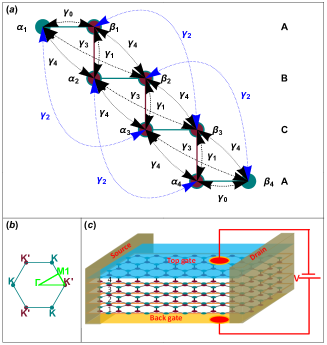
We consider a lattice of ABCA-TTLG consists of four coupled layersKoshino2010 ; Ben201301 , each with carbon atoms arranged on a honeycomb lattice, including pairs of inequivalent sites , , and in the top, center, and bottom layers, respectively. The layers are arranged as shown in Fig. 1(a) such that pairs of sites and , , and and , lie directly above or below each others. The different sublattices and are represented by darkred and teal solid balls, respectively. In order to write down an effective mass Hamiltonian, we adapt the Slonczewski-Weiss-McClure parameterization of tight-binding couplings of bulk graphite Dresselhaus200286 . We include parameters , , , and , where the intralayer coupling (), the interlayer coupling (), the interlayer coupling and (), the interlayer coupling between and (), the interlayer coupling and (). For typical values, we quote Dresselhaus200286 eV,eV, eV, eV and eV. These interatomic coupling parameters are depicted in Fig. 1(a). The contribution of the skew hopping parameter results in the so calledMcCann2006 ; McCann2007 trigonal warping, an effect occurring only at very low energy () which will be discussed in Sec III.2. The parameter has an even lower impact on the electronic properties, see Sec III.2. Therefore, we will often neglect these two -parameters in Sec III.1 and III.3. There is a degeneracy point at each of two inequivalent corners and of the hexagonal first Brillouin zone, also referred to as valleys, Fig. 1(b). Near the centre of each valley, there are eight electronic bands. In the basis the electronic properties for ABCA-TTLG are then obtained from the following Hamiltonian matrixKoshino2010
| (5) |
where the interlayer couplings and are given by
| (10) |
with are related to the skew hopping parameters, is the Fermi velocity in terms of the in-plane nearest neighbor hopping , is the lattice constant. The matrix describes the intralayer processes for ABCA-TTLG is
| (11) |
labeling the graphene layers, describe an external potential in each layers, is a momentum space representation of intersublattice hopping processes for electrons with wave vector . In the framework of a tight-binding approximation (see Sec. III.1), is given byHasegawa200613 ; Dietl200805 ; Wunsch200827
| (12) |
where and are basis vectors of the triangular Bravais lattice, in terms of the lattice constant , is the nearest-neighbor hopping energy (hopping between different sublattices), and the next nearest-neighbor hopping integral (hopping in the same sublattice). The angular dependence of in Eq. 12 is called trigonal warping because it leads to a deformation of the form of the Fermi line around the centre of each valley. This deformation increases with an increase of the absolute value of the wave vector. In ABCA-TTLG, a second cause of trigonal warping is the parameter describing direct interlayer coupling between and (), leading to an effective velocity . In the low-energy model (see Sec. III.2), is
| (13) |
where is the two dimensional momentum operator. The applied potential can be varied by gating the sample with top and back gates (see Fig. 1(c)). This is
| (14) |
where describes a potential difference between layers 1 and 4.
III Band structure
III.1 Tight-binding model
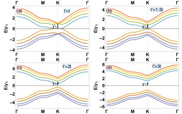
In order to calculate the full dispersion of ABCA-TTLG we numerically diagonalize the Hamiltonian Eq. (5). The resulting diagonal matrix then contains eight distinct entries corresponding to the energy bands compared with monolayer, AB-BL and ABC-TLG which contains two, four and six bands, respectively. These eight bands are plotted in Fig. 2, 3 and 4. In Fig. 2, we show the typical behavior of the band structure dependence of next-nearest-neighbor hopping for fixed nearest neighbor and applied potential . For the energy vanishes at two points located at the Dirac corners and of the hexagonal BZ spaced by (see Fig. 2(a)). For , the Dirac points approach each other, their distance varies as , the Dirac cones become anisotropic (deformed honeycomb lattice) (see Fig. 2(b)). For , the two Dirac points merge into a single point at (see Fig. 2(c)). For , a gap opened eV between the conduction and valance bands, and the two Dirac points coincide at (see Fig. 2(d)). We notice that for and the band structure of ABCA-TTLG in our Tight-binding model consists of a set of four pairs cubic of bands, one of them touching each other at the points and , and the other three crossing at the energy . These two bands intersect exactly at which corresponds to the special point in the reciprocal space of the hexagonal lattice. The insets of Fig. 2 show the zoom of the bands at the Dirac point and the deformation of hexagonal Brillouin zone (lattice) by variation of the next nearest-neighbor hopping .
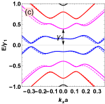
For a more understanding of the effects of the next nearest neighbors on band structure of ABCA-TTLG we show in Fig. 3 the bands for different values of along the lines in the first BZ. From this Figure it is very clear that the presence of the parameters (as increases) introduces a band gap on the band structure.
To illustrate the effects of the potential on the band structure of ABCA-TTLG in the tight-binding model we plot it versus the transverse wave vector in Fig. 4 for some values the potential height with . The Bravais lattice retains its shape even if is strong but contribute to the opening of a gap between the conduction and valence bands. Note that remains unchangeable. More interesting features appear when zooming into the low energy regime around the point see Sec. III.2.
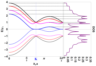
In Fig. 5, the influence of next-nearest-neighbor hopping on electronic DOS in ABCA-TTLG is shown. The DOS have a zero value at the Fermi energy and ten sharp van Hove singularities (VHS) appear at the onset of each subband. We also see, as in the spectrum, an apparent symmetry for positive and negative VHS in the DOS. This also implies zero-gap semiconductor with semi metallic behavior. In addition, sharp peaks in the DOS are observed, which are the characteristic signatures of the one-dimensional (1D) nature of conduction within a 1D system. We conclude that by varying , VHS can be brought to accessible energies, which is one of the important features of the ABCA-TTLG.
III.2 Low-energy model
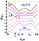
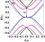
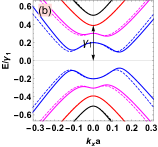


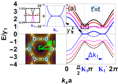
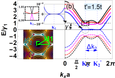
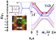
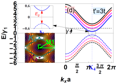
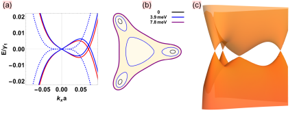
The band gap is an intrinsic property of semiconductors, which indeed hugely determines the transport and the optical properties. It should have a key role in modern device industry and technology. In this section, we focus on the sensitivity of the band structure of ABCA-TTLG at low-energy by varying the applied potential defined in Eq. 14 between the top and the bottom layer. Using similar approach as before, we show in Fig. 6 the 2D (upper row) band structure at point and the corresponding 3D plot (lower row) of the effective Hamiltonian derived from Eq. 5 where is given by Eq. 13. The potential is for the top and bottom layer. The dashed curves also account for the skew hopping parameters defined in Fig. 1(a) while the solid curve considers only nearest-neighbor interlayer hopping . It is clear that at high energy meV the effect of the skew hopping parameters and to these band structures depicted in Fig. 6 is negligible (see Fig. 7(a)). That is why we did not take into consideration their effects on the band gaps. Trigonal warping due to becomes particularly relevant at very low energy of the order of meV. Fig. 7(b)) shows contour plots of the lower electron band at , showing that the band is trigonally warped, and the contour splits into three pockets at low energy. The detailed band structure and its relation to the band parameters will be studied in the present sections.
For the spectrum consists of a set of four pairs cubic of bands, one of them touching each other at the point and the other three crossing at an energy above (below) , as shown in Fig. 6(a). However, for the location of the fundamental gap shifted, in BZ, from to finite values of , similar to what was observed in the gated multi-layer graphene Avetisyan200901 ; Avetisyan201032 (see Fig. 6(b, c)). From these figures, four pairs of bands hybridize and repel each other and a sizable band gap is created at , which could be opened and controlled by . The repelling of the two bands creates band gaps with . We denote the pair of highest (lowest) bands near the Dirac point as the conduction (valence) bands. Around and for , these bands exhibit several local maxima and minima as the potential difference is increased (see Fig. 6(b, c) and Tab. 1). Always they are symmetric with respect to . Therefore, the band gaps are strongly dependent on and are given by
| (15) | |||||
| (16) | |||||
| (17) | |||||
| (18) |
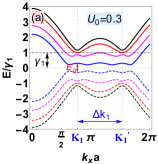
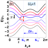
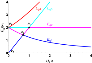
These four bands are illustrated in Fig. 8 which clearly define a better understanding of the band structure of ABCA-TTLG dependence on the band gap. The gaps are measured in units of . Our main result shows that the first band gap initially increases and falls as increased. is zero at ( point) and reaches a maximum eV as reaches V/Å ( point). The second band gap exhibits one local minima at V/Å ( point) and two local maxima who have the same gap energy eV at () and at V/Å (), and then remains constant. varies steadily until reaches V/Å () and then increases monotonically when increases. As long as increase the band gap continuously increased.
In general, for the ABCA-TTLG the coordinates of the points , , and illustrated in Fig. 8 are given by ), , and which are strongly dependent on gamma . We note that the behavior of the minimum band gap in ABCA-TTLG is similar to ABC-TLGKumar201101 ; Koshino2010 , which increases by increasing with band gaps below a critical value, and decreases with band gaps above this critical value. By contrast, in AB-BLGKoshino2010 ; Koshino200910 the situation is completely different because increases as increases.
III.3 Two-band approximation model
The same as for AB-BLG and ABC-TLG, it is possible to introduce the effective two-band description at low energy approximation for the ABCA-TTLG. This two component Hamiltonian was derived in vanduppen2013 ; MacDonald2008 ; Nakamura and is only valid as long as the electronic density is low enough, that is, when the Fermi energy is much smaller than (). We use similar analysis to that previously described in Ref.vanduppen2013 , which yields the HamiltonianBen201301
| (21) |
where . In the two band approximation model, the Hamiltonian in Eq. 21 has a plane wave solution given by two propagating waves, one right and one left moving, and six evanescent waves. The wave vectors of these plane waves are the solutions of the equation
| (22) |
where is the transverse wave vector, is the angle of the wave vector with the normal chosen perpendicular to the pn junction. The solution of this equation is with four different values for and the dispersion relation is given by
| (23) |
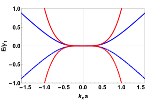
The validity of this approximation is presented in Fig. 9 where we show the dispersion relation obtained in the low energy model (blue curves ) and the dispersion relation obtained from the Hamiltonian in the two bands model (red curves). We clearly see that for the two band spectrum for the low-energy model are in good agreement with the two band spectrum for low energy Eq. 21.
IV Transmission probability
In this paragraph, we focus on the transmission probability through a pn junction in the two band approximation model (Eq. 21) and adopt the same approach used by Ben et al. Ben201301 . The eigenstates of these Hamiltonians are eight-component spinors consisting of a superposition of four times two oppositely propagating or evanescent waves characterized by four distinct wave vectors denoted as , , and . For a system that is translational invariant in the direction, the energy and dependence on these wave vectors can be found from
| (24) |
and is given by Eq. 21. The eigenstates solution can be written as a product of matrices,
| (25) |
where is a matrix expressing the relative importance of the different components of the spinor that can be constructed by solving the Dirac equation . The matrix is given by
| (26) |
where and the matrix is
| (27) |
due to the translational symmetry in the direction, the dependency is incorporated in an exponential phase factor and will be ignored from this point on. We denote the four component vector as
| (28) |
where the subscript refers to the corresponding wave vector and the superscript plus/minus indicates the right/left propagating or evanescent states. The boundary conditions of the system under consideration will determine which of the components of vector are zero. To find the transmission probability for a pn junction, one has to equate the plane wave solutions and all the derivatives up to order of the region before the junction (region I) with those of the region behind it (region II) at the junction’s edge at , giving rise to a set of four two component equations Ben201301
| (29) |
where the matrix is evaluated at . This leads to the matrix
| (30) |
Normalizing the incident wave on the right propagating wave before the junction by putting and applying boundary conditions for to suppress the non normalizable plane wave functions. Therefore, the transmission and the reflection probabilities are given by
| (31) |
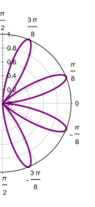
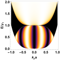
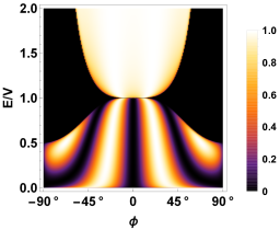
The numerical results of the transmission probability for ABCA-TTLG is depicted in Fig. 10. At normal incidence, i.e. (), the transmission equals zero independently of energy or height of the step. There are four high-transmission regions for (see Fig. 10 bottom row), which are typical for tetralayer graphene, shifted away from each other and each one forms a Klein (KT) and anti-Klein (AKT) tunneling region. The expected angles () for KT and () for ATK (see Fig. 10 top row), which are in agreement with those obtained by Ben et al. Ben201301
V Conclusion
In conclusion, we have analyzed the band structure, DOS and transmission in ABCA-TTLG. Tight binding Hamiltonian containing nearest-neighbors and , effective Hamiltonian and two band approximation Hamiltonian with interlayer potential difference parameters have been employed. The expressions of band gaps around the are obtained. Interlayer potential difference is found to be responsible for generating band gaps near Dirac point in ABCA-TTLG. The next nearest-neighbor hopping breaks the symmetry of Bravais lattice and the corresponding BZ (e.g. its high symmetry points such as corners and move) and the Dirac points may merge and move away from the high symmetry points. This gives rise to 1D-like VHS in the DOS. Using the two-band approximation model, the KT and AKT angles are obtained.
VI Acknowledgement
The generous support provided by the Saudi Center for Theoretical Physics (SCTP) is highly appreciated by all authors.
Références
- (1) M. Aoki and H. Amawashi, Solid State Commun. 142, 123 (2007).
- (2) M. S. Dresselhaus and G. Dresselhaus, Advances in Physics 51, 186 (2002).
- (3) M. Koshino and T. Ando, Solid State Commun. 149, 1123 (2009).
- (4) S. H. Jhang, M. F. Craciun, S. Schmidmeier, S. Tokumitsu, S. Russo, M. Yamamoto, Y. Skourski, J. Wosnitza, S. Tarucha, J. Eroms, and C. Strunk Phys. Rev. B 84, 161408(R) (2011).
- (5) M. Koshino, Phys. Rev. B 81, 125304 (2010).
- (6) C. H. Lui, Z. Q. Li, Z. Y. Chen, P. V. Klimov, L. E. Brus, and T. F. Heinz, Nano Lett. 11, 164 (2011).
- (7) S. Latil and L. Henrard, Phys. Rev. Lett. 97, 036803 (2006).
- (8) M. Koshino, Phys. Rev. B 81, 125304 (2010).
- (9) A. I. Cocemasov, D. L. Nika, and A. A. Balandin, Phys. Rev. B 88, 035428 (2013).
- (10) K. F. Mak, J. Shan, and T. F. Heinz, Phys. Rev. Lett. 104, 176404 (2010).
- (11) F. Guinea, A. H. C. Neto, and N. M. R. Peres, Phys. Rev. B 73, 245426 (2006).
- (12) A. A. Avetisyan, B. Partoens, and F. M. Peeters, Phys. Rev. B 80, 195401 (2009).
- (13) A. A. Avetisyan, B. Partoens, and F. M. Peeters, Phys. Rev. B 81, 115432 (2010).
- (14) C. L. Lu, C. P. Chang, Y. C. Huang, R. B. Chen, and M. L. Lin, Phys. Rev. B, 73, 144427 (2006).
- (15) B. Van Duppen and F. M. Peeters, Europhys. Lett. 102, 27001 (2013).
- (16) Raad Chegel, Synthetic Metals 223, 172 (2017).
- (17) Lei Hao and L. Sheng, Solid State Commun. 149, 1962 (2009).
- (18) S. Bala Kumar and Jing Guo, Appl. Phys. Lett. 98, 222101 (2011).
- (19) E. McCann and V. I. Fal’ko, Phys. Rev. Lett. 96, 086805 (2006).
- (20) E. McCann, D. S. L. Abergel, and V. I. Fal’ko, Solid State Commun. 75, 193402 (2007).
- (21) Y. Hasegawa, R. Konno, H. Nakano, and M. Kohmoto Phys. Rev. B 74, 033413 (2006).
- (22) P. Dietl, F. Piéchon, and G. Montambaux, Phys. Rev. Lett. 100, 236405, (2008).
- (23) B. Wunsch, F. Guinea, and F. Sols, New J. Phys. 10, 103027 (2008).
- (24) M. Koshino, New J. Phys. 11 095010 (2009).
- (25) B. Van Duppen, S. H. R. Sena, and F. M. Peeters, Phy. Rev. B 87, 195439 (2013).
- (26) H. Min and A. H. MacDonald, Phys. Rev. B 77, 155416 (2008).
- (27) M. Nakamura and L. Hirasawa, Phys. Rev. B 77, 045429 (2008).