Two-dimensional plasmonic waveguides for nanolasing and four-wave mixing
Abstract
Plasmonic waveguides are an essential element of nanoscale coherent sources, including nanolasers and four-wave mixing (FWM) devices. Here we report how the design of the plasmonic waveguide needs to be guided by the ultimate application. This contrasts with traditional approaches in which the waveguide is considered in isolation. We find that hybrid plasmonic waveguides, with a nonlinear material sandwiched between the metal substrate and a high-index layer, are best suited for FWM applications, whereas metallic wedges are preferred in nanolasers. We also find that in plasmonic nanolasers high-index buffer layers perform better than more traditional low-index buffers.
1Shenzhen Institutes of Advanced Technology, Chinese Academy of Sciences, Shenzhen 518055, Guangdong Province, China
2Institute of Photonics and Optical Science (IPOS), School of Physics, The University of Sydney, NSW 2006, Australia
3The University of Sydney Nano Institute, The University of Sydney, NSW 2006, Australia
*Corresponding author: gy.li@siat.ac.cn
1 Introduction
Waveguide-based nanoscale coherent light sources are essential to nanophotonic circuits in diverse applications including high-speed on-chip interconnects [1], quantum information processing [2], chemical and biomedical sensing [3]. Plasmonic waveguides are key elements of such devices since they allow subwavelength light confinement, and hence greatly enhanced light-matter interactions [4, 5]. We consider two different classes of plasmonic-waveguide based coherent nanoscale light sources: nanolasers [6, 7, 8], and nonlinear devices for frequency conversion, specifically degenerate four-wave mixing (DFWM) [9, 10, 11].
Although requirements on plasmonic waveguides for nanolasing and for DFWM applications are distinct, and are also different from those for pure waveguiding applications, plasmonic waveguides are traditionally characterized by their attenuation and by their mode confinement, independently of the ultimate application [12]. For example, after comparing four typical plasmonic waveguides, Oulton et al. found that hybrid plasmonic metal/low-index insulator/high-index semiconductor/air (known as MISA) configurations, exhibit low attenuation loss and high mode confinement [12]. Subsequently, MISA-based devices have been widely used in plasmonic nanolasers [13, 14, 15, 16, 17, 18]. Encouraged by the attractive waveguiding characteristics, as well as the successful applications in nanolasers, the use of hybrid plasmonic waveguides has been extended to nonlinear applications [19, 20, 9, 21], but without a rigorous comparison to other types of plasmonic waveguides.
We recently developed a comprehensive theory for the design and analysis of plasmonic waveguides for nanolasing, and applied this theory, after a slight modification, to the waveguide design for plasmonic FWM devices as well [22]. Our exploration based on one-dimensional (1D) plasmonic waveguide geometries not only provides deep understanding of currently used designs, but also led to potentially superior structures, with the potential to address longstanding challenges in plasmonic nanolasers. Although one- and two-dimensional plasmonic waveguides share the same physics, edge effects introduced by additional dimension may change the modal properties of plasmonic waveguides [23] and accordingly the nanolasing or DFWM performance.
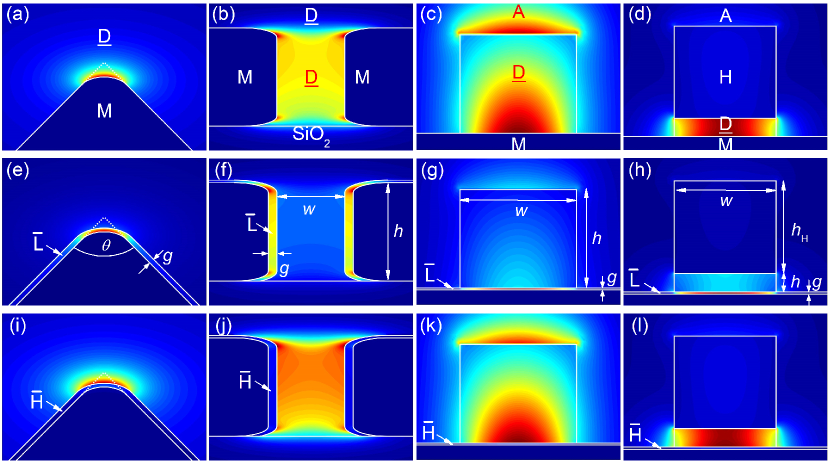
Here we characterize four realistic 2D plasmonic waveguides for nanolasing and DFWM applications. The four structures, illustrated in Figure 1(a)–(d), are: a metallic wedge waveguide, a metal-slot waveguide, a dielectric loaded surface plasmon polariton (DLSPP) waveguide, and a hybrid plasmonic waveguide.
The outline of this paper is as follows. In Section 2 we compare the nonlinear contributions due to the metal with that due to a nonlinear dielectric, and show that the nonlinearity of the metal can be ignored in these DFWM devices. In Section 3 we then briefly introduce the theory we previously developed [22], highlighting the characteristic measures of plasmonic waveguides for nanolasing and DFWM applications. The characteristics of plasmonic waveguides for use in nanolasers and DFWM devices can then be compared and understood in Section 4, allowing us to identify the desirable plasmonic waveguides for these applications. Section 5 includes a discussion of the effects of the refractive index of buffer layers that are used in nanolasers to avoid quenching.
2 Nonlinear contributions from constituent materials
In nonlinear plasmonic waveguides all constituent materials contribute to some degree to the overall nonlinearity. However, since our theory [22] assumes that the contribution from a highly nonlinear dielectric dominates, we need to validate this assumption before we apply this theory to a specific plasmonic waveguide structure. This is especially important since recent studies showed that the third-order nonlinear susceptibility of metals can be large at optical wavelengths [24, 25, 26].
To carry out this comparison we follow the approach by Baron et al. for surface plasmon polaritons [27], which we recently extended to more complicated 1D geometries [28]. For simplicity, we take only one dielectric to be highly nonlinear, and neglect nonlinear contributions from other dielectrics in the plasmonic waveguide. The ratio of the nonlinear contribution from the highly nonlinear dielectric and that from metal can be written as [28]
| (1) |
where we used , is the modal electric field, is the third-order nonlinear susceptibility, and “D” and “M” refer to the highly nonlinear dielectric and the metal, respectively. The integrals are taken over the respective media.
The four 2D plasmonic waveguides we consider are shown in Figures 1(a)–(d), and are denoted as “MD” wedge, “MDM” slot, “MDA” DLSPP, and “MDHA” hybrid plasmonic waveguide, respectively. These denotations indicate the type of layers encountered in the direction perpendicular to the metal surface. In addition to “M” and “D” defined above, “A” means air, and “H” is a dielectric that has higher refractive index than “D”. For all these waveguides, we consider only the fundamental plasmonic mode. For the “MD” wedge, we take the radius of the metallic curvature to be nm [29].
Throughout this work, we consider , and take metal to be silver with linear refractive index [30], and third-order nonlinear susceptibility [31]. We consider the highly nonlinear dielectric to be DDMEBT with linear refractive index , nonlinear refractive index [32], and thus . The field profiles of the fundamental modes are calculated using the finite element method as implemented in COMSOL, and are shown in Figure 1.
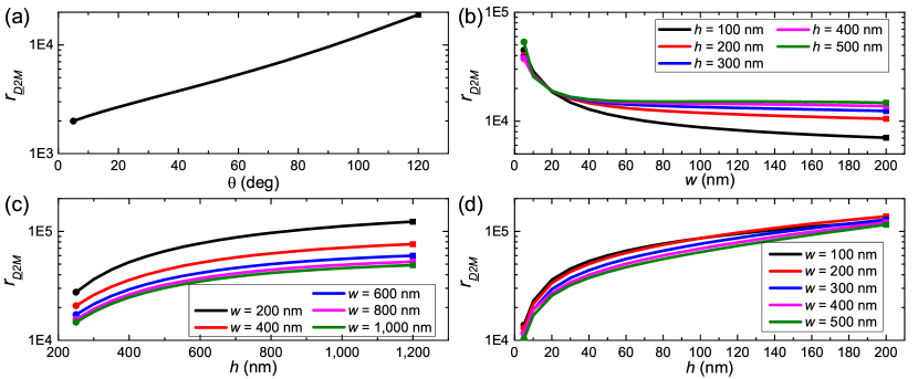
Figure 2 shows that for all the four plasmonic waveguides under study, . This means that the nonlinear contribution from metal is negligible compared to that from the highly nonlinear dielectric. This is because although , we find since the electric field is mainly confined to the highly nonlinear dielectric region (see Figure 1(a)–(d)). This conclusion does not change even if silver is replaced by gold, which, according to a recent report [26] has a nonlinear susceptibility as large as .
3 Characteristic measures for plasmonic nanolasers and DFWM devices
The theory we developed [22] shows that plasmonic waveguides used as nanolasers or as DFWM devices can be measured using a set of two characteristic dimensionless parameters. Surprisingly, these two sets of parameters are very similar, and each provides clear physical insights. We discuss these now.
The first characteristic measure for plasmonic waveguides that applies to both devices, is the effective area normalized by the diffraction-limited area , i.e., . Here is defined as [22]
| (2) |
where are the modal fields, indicates the maximum over the active medium which has linear refractive index . The active medium D denotes the gain medium in nanolasers, and the highly nonlinear layer in DFWM devices.
In nanolasers, measures the maximum Purcell factor of a waveguide mode [33], , through , whereas in DFWM devices, measures the driving power for which the nonlinear refractive index change of the highly nonlinear material saturates and reaches its maximum value , via . Here is the maximum allowed intensity under plane wave illumination before optical damage occurs.
The second dimensionless measure for plasmonic waveguides in a nanolaser is
| (3) |
where is the threshold gain, i.e., the material gain needed to compensate the modal loss and to achieve lasing. Further, , and is the relative permittivity of metal.
The second dimensionless measure for plasmonic waveguide in a DFWM device is
| (4) |
where is the Figure of Merit, and expresses the field uniformity in the highly nonlinear medium.
A low-threshold waveguide-based nanolaser requires (i) enhanced spontaneous emission that is efficiently coupled into the guided mode, which is equivalent to requiring the mode to have a high Purcell factor in order to make full use of the gain medium; and (ii) a low threshold gain . Optimizing a nanoscale DFWM device requires (i) that the maximum nonlinearity of the material, i.e., the maximum achievable nonlinear index change is reached at a low driving power, ; and (ii) a large Figure of Merit in order to achieve a high conversion efficiency. We showed earlier that the maximum achievable conversion efficiency is [34], which is defined as the ratio of the output idler power to the input signal power. Requirements (i) for both types of devices are equivalent to a small effective area , whereas requirements (ii) for both devices correspond to large and large .
We can further write
| (5) | |||||
| (6) |
Here the gain confinement factor [35] and the nonlinear effectiveness [28] can be written as
| (7) |
where is the vacuum impedance, and accounts for modal loss [34].
Comparing Eqs (3) and (4), or Eqs (7), we find that the only difference between or for plasmonic nanolasers and or for plasmonic DFWM devices is that the latter has an additional factor in the integral kernel of the numerator. This factor highlights the importance of field uniformity in the active medium for nonlinear DFWM applications.
Compared with the parameters and for characterizing plasmonic waveguides for pure waveguiding applications, it is clear that the measures for nanolasing and DFWM, and or , also include or , corresponding to the overlap between the mode field and the gain or nonlinear medium. Therefore, plasmonic waveguides that are optimized for waveguiding applications may be suboptimal for nanolasing or DFWM.
4 Characteristics for nanolasing and DFWM
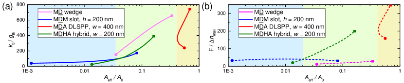
Figure 3 compares the nanolasing and DFWM characteristics of the four 2D plasmonic waveguides from Figure 1(a)–(d). We now discuss these in turn. At this stage we neglect the quenching effects in plasmonic nanolasers; we shall consider these in Section 5.
4.1 MD wedge waveguide
Figure 3(a) shows that, as the wedge angle for MD wedge waveguides increases from to , increases from to , thus remaining below the diffraction limit (). Simultaneously, increases from to . In other words, the maximum modal Purcell factor decreases from to , while the gain threshold decreases from to . On the other hand, increases only slightly and remains below . Thus the maximum achievable DFWM conversion efficiency would be low: for , making MD wedge waveguides less suited for DFWM applications.
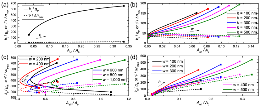
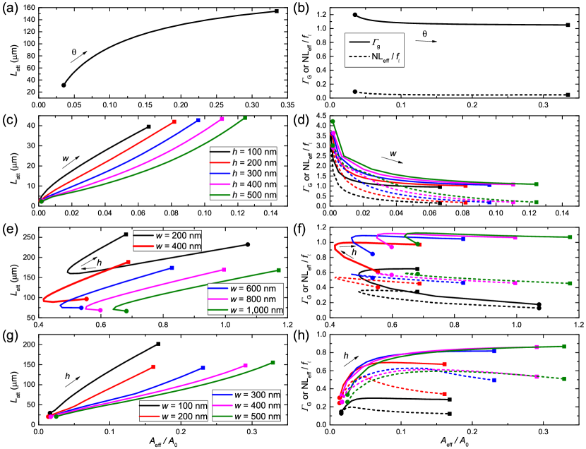
The large difference between the nanolasing characteristics ( versus ) and the DFWM characteristics ( versus ) can be explained by (3). Although the MD wedge waveguide combines long propagation length and small effective area , as shown by Figure 4(a), making it particularly attractive for waveguiding applications, the gain confinement factor is large whereas the nonlinear effectiveness is very low, as shown by Figure 4(b). This difference comes from the factor, which is important for MD wedge waveguides because of the extremely nonuniform modal electric field of the mode (see Figure 1(a)).
4.2 MDM slot waveguide
Figure 3(b) compares the nanolasing and DFWM characteristics of MDM slot waveguides. can reach the deep subdiffraction regime () for narrow slot widths of nm, making the MDM slot waveguide particularly attractive for achieving ultra-high modal Purcell factor in nanolasing applications or ultra-low driving power in nonlinear DFWM applications. For narrow slots and have close values. As the slot becomes wider, increases whereas decreases in general.
These characteristics can also be understood using (3), where , and are shown in Figures 4(c)(d). As the slot width increases, more electric energy is confined to the slot, resulting in less attenuation loss or longer . However, the gain confinement factor and the nonlinear effectiveness both decrease unexpectedly; and more strikingly, they can be much larger than unity for narrow slot widths, indicating that the modal gain/nonlinearity is much larger than the gain/nonlinearity of the bulk material. This behaviour arises from slow light effects. We have shown [28] that both and can be factorized in an intuitive way as the product of factors that express the effects of losses, of slow light, and of the electric energy overlap with the active medium,
| (8) | |||||
| (9) |
Here is the slow-down factor, with the velocity of a plane wave in bulk and the energy velocity of the mode. Here the mode power , and the mode energy . () quantifies the fraction of electric energy in the gain material, and () quantifies fraction of the electric energy ratio in the nonlinear material, weighted by the field uniformity (). Here
| (10) | |||||
| (11) |
where the approximations originate from . For metal, which is dispersive, , whereas for the active material which is taken to be dispersionless. Equations (10) and (11) imply that a large requires strong electric energy confinement in the gain material, whereas a large requires strong and uniform electric energy confinement in the nonlinear material. For MDM slot waveguides with narrow slots, the slow-down factor is very large, while the electric energy is strongly and uniformly confined to the slot [28], leading to larger-than-unity and . As the slot width increases, strongly decreases, while and changes slightly [28], resulting in decreasing and .
As the MDM slot becomes deeper, i.e., as increases, , and all slightly increase. The argument is similar to that for varying , and is thus not further discussed here.
4.3 MDA DLSPP waveguide
Figure 3(c) shows that for MDA DLSPP waveguides first decreases and then increases as the dielectric height increases. This can be understood following Holmgaard and Bozhevolnyi [36]: decreasing the height of the D layer squeezes the field inside the D region, but this behaviour does not continue indefinitely. Thus decreases until reaching a minimum; decreasing the D height further results in a rapid increase in the field outside the D region, resulting in increasing . Similarly, first decreases and then increases as the dielectric height increases, as shown by Figure 4(e). However, because of the complicated compromise between and (or ) in Figure 4(f), (or ) increases monotonously with height.
For MDA DLSPP waveguides, the distinct characteristics for waveguiding applications, i.e., versus , and for nanolasing or DFWM applications, i.e., or versus , clearly illustrate that the plasmonic waveguide optimized for waveguiding applications may not be optimal for nanolasing or DFWM. For example, Figure 4(e) shows that MDA DLSPP waveguides with nm generally have better waveguiding performance than those with nm, i.e., have longer propagation lengths under the same confinement. However, because the latter have much larger or , the net effect is that MDA waveguides with nm generally have better nanolasing or DFWM performance.
4.4 MDHA hybrid plasmonic waveguide
For MDHA hybrid plasmonic waveguides, Figure 3(d) shows that , and all increase, with increasing height of the active medium . This is because strongly increases, whereas first increases and then saturates, and first increases and then drops, as shown by Figures 4(g) and 4(h), respectively. The differences between and , and thus between and are relatively small. This is because even for large hight , the electric field in the active medium is relatively uniform, as shown in Figure 1(d).
Similar to MDA DLSPP waveguides, the waveguiding characteristics and the nanolasing or DFWM characteristics for MDHA waveguides may be quite different. For example, Figure 4(g) shows that MDHA waveguides with nm have better waveguiding performance but worse nanolasing or DFWM performance than those with nm. The reason, again, is because the latter have much larger or , as shown in Figure 4(h).
4.5 Comparison of four plasmonic waveguides
Having understood the nanolasing and DFWM characteristics of all four plasmonic waveguide structures, we now summarize their performance in Figure 5. Depending on the effective area, we define the deep-, moderate- and near-subdiffraction regions, as indicated by blue, green, and yellow in Figure 5.
Figure 5 shows that MDM slot waveguides perform best in the deep-subdiffraction region since it combines the highest modal Purcell factor in nanolasing, and the lowest driving power in DFWM applications. In the moderate-subdiffraction region, the MD wedge waveguide has the best performance for use as a nanolaser since it combines high modal Purcell factor and low gain threshold (Figure 5(a)), whereas the MDHA hybrid waveguide performs best for use as a DFWM device by combining low driving power and high conversion efficiency (Figure 5(b)). This is broadly consistent with the conclusion reached based on the waveguiding characteristics only [12]. As a example, metallic wedge waveguides with integrated reflectors and precisely placed colloidal quantum dots have been used to achieve high-quality quantum emitters [29]. In the near-subdiffraction region, or when we can tolerate a modest modal Purcell factor for nanolasers or high driving power for DFWM devices, the MDA DLSPP performs best.
In our previous work on 1D plasmonic waveguides [22], the 1D counterpart of the MD wedge waveguide is the 1D MD surface plasmon polariton (SPP) waveguide. Therefore, the pink curve in Figure 5 reduces to a point for its 1D counterpart [22]. Therefore, in the moderate-subdiffraction region the best performing structure for both nanolasing and DFWM applications is the MDHA hybrid plasmonic waveguide. In contrast, in the deep-, and the near-subdiffraction regions the wedge waveguide is the best performing 2D plasmonic waveguide configurations for both nanolasing and for DFWM, in line with our conclusions based on a 1D analysis [22].
5 Effect of buffer layers in plasmonic nanolasers
For plasmonic nanolasers, a buffer layer needs to be included between the metal “M” and the gain material “D” so as to avoid quenching. We recently showed that a high-index buffer outperforms a low-index buffer for 1D plasmonic waveguides, and illustrated the 2D extension of this with a specific MDA 2D structure [22]. We now show that this conclusion also applies to the four 2D plasmonic waveguides studied in this work.
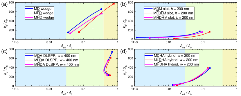
Figure 6 shows that for all four 2D plasmonic waveguides the use of a high-index (indicated as “” between “M” and “D”) buffer layer results in a smaller effective area than a low-index (“”) buffer layer for the same lasing threshold. The thicknesses of all buffer layers, which can be deposited with atomic layer deposition or sputtering, are taken to be nm. In other words, in plasmonic nanolasers based on the four 2D plasmonic waveguides, a high-index buffer layer outperforms a low-index one. This conclusion is consistent with that for 1D configurations [22]. The reason is very similar: the use of a “” buffer confines most of the electric field to the buffer layer (second row of Figure 1), thus greatly decreasing the gain confinement factor, although the loss is also reduced. In contrast, “” buffers confine most of the electric field to the gain “D” medium (third row of Figure 1), thus greatly increasing the gain confinement factor, which outweighs the slightly larger loss [22].
6 Conclusions
In conclusions, we have investigated the nanolasing and DFWM characteristics of four 2D plasmonic waveguides. Our analysis shows that the MDM slot waveguide is the best performing structure for achieving the highest modal Purcell factor in nanolasing or the lowest driving power in DFWM applications. The MD wedge waveguide has the best performance for use as a nanolaser by combimning high model Purcell factor and low gain threshold, whereas the MDHA hybrid waveguide performs best for use as a DFWM device for combing low driving power and high conversion efficiency. We also show that for plasmonic nanolasers that require a buffer layer between the metal and the gain medium, high-index buffers outperform conventional low-index buffers. We expect this work will advance the design and understanding of plasmonic waveguides that are used in nanolasers and nanoscale DFWM devices.
Acknowledgments
This work was supported by the School of Physics, the University of Sydney, by the Shenzhen Research Foundation (Grant No. JCYJ20180507182444250), and by the State Key Laboratory of Advanced Optical Communication Systems and Networks, China (No. 2019GZKF2).
References
- [1] D. A. B. Miller. Device requirements for optical interconnects to silicon chips. Proc. IEEE, 97:1166–1185, 2009.
- [2] T. G. Tiecke et al. Nanophotonic quantum phase switch with a single atom. Nature (London), 508:241–244, 2014.
- [3] C. Monat, P. Domachuk, and B. J. Eggleton. Integrated optofluidics: A new river of light. Nat. Photon., 1:106–114, 2007.
- [4] D. J. Bergman and M. I. Stockman. Surface plasmon amplification by stimulated emission of radiation: quantum generation of coherent surface plasmons in nanosystems. Phys. Rev. Lett., 90:027402, 2003.
- [5] M. Kauranen and A. V. Zayats. Nonlinear plasmonics. Nat. Photon., 6:737–748, 2012.
- [6] R.-M. Ma, R. F. Oulton, V. J. Sorger, and X. Zhang. Plasmon lasers: Coherent light source at molecular scales. Laser Photon. Rev., 7:1–21, 2013.
- [7] S. Gwo and C.-K. Shih. Semiconductor plasmonic nanolasers: Current status and perspectives. Rep. Prog. Phys., 79:086501, 2016.
- [8] A. Yang, D. Wang, W. Wang, and T. W. Odom. Coherent light sources at the nanoscale. Annu. Rev. Phys. Chem., 68:83–99, 2017.
- [9] F. J. Diaz et al. Sensitive method for measuring third order nonlinearities in compact dielectric and hybrid plasmonic waveguides. Opt. Express, 24:545–554, 2016.
- [10] V. Kravtsov, R. Ulbricht, J. M. Atkin, and M. B. Raschke. Plasmonic nanofocused four-wave mixing for femtosecond near-field imaging. Nat. Nanotech., 11:459–464, 2016.
- [11] M. P. Nielsen, X. Shi, P. Dichtl, S. A. Maier, and R. F. Oulton. Giant nonlinear response at a plasmonic nanofocus drives efficient four-wave mixing. Science, 358:1179–1181, 2017.
- [12] R. F. Oulton, G. Bartal, D. F. P. Pile, and X. Zhang. Confinement and propagation characteristics of subwavelength plasmonic modes. New J. Phys., 10:105018, 2008.
- [13] R. F. Oulton et al. Plasmon lasers at deep subwavelength scale. Nature (London), 461:629–632, 2009.
- [14] R.-M. Ma, R. F. Oulton, V. J. Sorger, G. Bartal, and X. Zhang. Room-temperature sub-diffraction-limited plasmon laser by total internal reflection. Nat. Mater., 10:110–113, 2011.
- [15] Y.-J. Lu et al. Plasmonic nanolaser using epitaxially grown silver film. Science, 337:450–453, 2012.
- [16] T. P. H. Sidiropoulos et al. Ultrafast plasmonic nanowire lasers near the surface plasmon frequency. Nat. Phys., 10:870–876, 2014.
- [17] Q. Zhang et al. A room temperature low-threshold ultraviolet plasmonic nanolaser. Nat. Commun., 5:4953, 2014.
- [18] H. Yu et al. Organic-inorganic perovskite plasmonic nanowire lasers with a low threshold and a good thermal stability. Nanoscale, 8:19536–19540, 2016.
- [19] J. Zhang, P. Zhao, E. Cassan, and X. Zhang. Phase regeneration of phase-shift keying signals in highly nonlinear hybrid plasmonic waveguides. Opt. Lett., 38:848–850, 2013.
- [20] A. Pitilakis and E. E. Kriezis. Highly nonlinear hybrid silicon-plasmonic waveguides: Analysis and optimization. J. Opt. Soc. Am. B, 30:1954–1965, 2013.
- [21] F. J. Diaz, G. Li, C. M. de Sterke, B. T. Kuhlmey, and S. Palomba. Kerr effect in hybrid plasmonic waveguides. J. Opt. Soc. Am. B, 33:957–962, 2016.
- [22] G. Li, S. Palomba, and C. M. de Sterke. Theory of waveguide design for plasmonic nanolasers. Nanoscale, 10:21434–21440, 2018.
- [23] Z. Han and S. I. Bozhevolnyi. Radiation guiding with surface plasmon polaritons. Rep. Prog. Phys., 76:016402, 2013.
- [24] A. Marini, M. Conforti, G. Della Valle, H. W. Lee, Tr. X. Tran, W. Chang, M. A. Schmidt, S. Longhi, P. St. J. Russell, and F. Biancalana. Ultrafast nonlinear dynamics of surface plasmon polaritons in gold nanowires due to the intrinsic nonlinearity of metals. New J. Phys., 15:013033, 2013.
- [25] R. W. Boyd, Z. Shi, and I. De Leon. The third-order nonlinear optical susceptibility of gold. Opt. Commun., 326:74–79, 2014.
- [26] H. Qian, Y. Xiao, and Z. Liu. Giant kerr response of ultrathin gold films from quantum size effect. Nat. Commun., 7:13153, 2016.
- [27] A. Baron, S. Larouche, D. J. Gauthier, and D. R. Smith. Scaling of the nonlinear response of the surface plasmon polariton at a metal/dielectric interface. J. Opt. Soc. Am. B, 32:9–14, 2015.
- [28] G. Li, C. M. de Sterke, and S. Palomba. Fundamental limitations to the ultimate kerr nonlinear performance of plasmonic waveguides. ACS Photon., 5:1034–1040, 2018.
- [29] S. J. P. Kress et al. Wedge waveguides and resonators for quantum plasmonics. Nano Lett., 15:6267–6275, 2015.
- [30] P. B. Johnson and R. W. Christy. Optical constants of the noble metals. Phys. Rev. B, 6:4370–4379, 1972.
- [31] R. W. Boyd. Nonlinear Optics. Academic, Orlando, 3rd edition, 2008.
- [32] B. Esembeson, M. L. Scimeca, T. Michinobu, F. Diederich, and I. Biaggio. A high-optical quality supramolecular assembly for third-order integrated nonlinear optics. Adv. Mater., 20:4584–4587, 2008.
- [33] V. J. Sorger et al. Strongly enhanced molecular fluorescence inside a nanoscale waveguide gap. Nano Lett., 11:4907–4911, 2011.
- [34] G. Li, C. M. de Sterke, and S. Palomba. Figure of merit for Kerr nonlinear plasmonic waveguides. Laser Photon. Rev., 10:639–646, 2016.
- [35] J. T. Robinson, K. Preston, O. Painter, and M. Lipson. First-principle derivation of gain in high-index-contrast waveguides. Opt. Express, 16:16659–16669, 2008.
- [36] T. Holmgaard and S. I. Bozhevolnyi. Theoretical analysis of dielectric-loaded surface plasmon-polariton waveguides. Phys. Rev. B, 75:245405, 2007.