Enhanced light-matter interaction in an atomically thin semiconductor coupled with dielectric nano-antennas
Abstract
Unique structural and optical properties of atomically thin two-dimensional semiconducting transition metal dichalcogenides enable in principle their efficient coupling to photonic cavities with optical modes volumes close to or below the diffraction limit. Recently, it has become possible to make all-dielectric nano-cavities with reduced mode volumes and negligible non-radiative losses. Here, we realise low-loss high-refractive-index dielectric gallium phosphide (GaP) nano-antennas with small mode volumes coupled to atomic mono- and bilayers of WSe2. We observe a photoluminescence enhancement exceeding 104 compared with WSe2 placed on planar GaP, and trace its origin to a combination of enhancement of the spontaneous emission rate, favourable modification of the photoluminescence directionality and enhanced optical excitation efficiency. A further effect of the coupling is observed in the photoluminescence polarisation dependence and in the Raman scattering signal enhancement exceeding 103. Our findings reveal dielectric nano-antennas as a promising platform for engineering light-matter coupling in two-dimensional semiconductors.
Monolayer semiconducting transition metal dichalcogenides (TMDs) Mak2016 such as WSe2 exhibit bright excitonic luminescence and strong absorption at room temperature with potential for photonic applications Wang2017 ; Mueller2018 . An important property favouring integration in devices is their compatibility with a wide range of substrates. So far, photonic device demonstrations include monolayer TMDs coupled to nano-cavities in photonic crystals Wu2015 ; Zhang2018a , nanobeam waveguides Li2017a and to microdisk cavities Salehzadeh2015 . TMD monolayers and van der Waals heterostructures Geim2013 comprised of vertically stacked atomic layers of TMDs, hexagonal boron nitride and graphene have been integrated in Fabry-Perot microcavities Dufferwiel2015 ; Sidler2016 . These devices provide photonic modes with relatively high quality factors, , in the range of 100s to 1000s. Despite the coupling to TMD monolayers via the relatively weak evanescent field, lasing in hybrid TMD-dielectric cavities has been observed Wu2015 ; Li2017a ; Salehzadeh2015 . Moreover, the strong light-matter interaction regime has been realized in optical microcavities Dufferwiel2015 ; Sidler2016 ; Liu2015 ; Schneider2018 and photonic crystals Zhang2018a , where atomic layers of 2D TMDs were placed at the anti-node of the photonic mode. Most of these devices relied on confining electromagnetic fields in diffraction-limited volumes, , in order to increase the spontaneous emission rate by the Purcell enhancement factor , which scales as . Whereas the high has been readily realized, provided by these structures is relatively large, leading to modest values of . Most of these devices also show a reduction of the light intensity compared with bare TMD monolayers, explained by the presence of fast non-radiative processes in the currently available TMDs, where the quantum yield is typically below 0.1% Amani2015 .
The effective volume of the optical mode can be reduced below the diffraction limit in plasmonic nano-cavities and nano-antennas Maier ; Koenderink2017 . By coupling semiconducting TMDs to such plasmonic structures, large photoluminescence (PL) enhancements Kern2015 ; Lee2015 ; Butun2015 ; Wang2016c ; Tahersima2017 ; Cheng2017 , strong light-matter coupling Kleemann2017 ; Wen2017 ; Cuadra2018 , brightening of the dark excitonic states Park2017a , and modification of optical properties of quantum light emitters Luo2018 ; Cai2018 have been observed. In some of these reports, special care had to be taken to overcome optical losses in metallic plasmonic structures by introducing a few nm dielectric spacer separating the TMD layer Tahersima2017 ; Cheng2017 ; Krasnok2018a . This turns out to be particularly important to suppress quenching for quantum light emitters Luo2018 ; Cai2018 .
Recently, it has also been shown that high-refractive-index dielectric nano-antennas can provide confined optical modes with strongly reduced mode volumes Caldarola2015 ; Kuznetsov2016 ; Cambiasso2017a ; Mignuzzi2019 ; Cihan2018 ; Lepeshov2018a . The main advantages of such structures are low non-radiative losses induced in the coupled light emitting material Caldarola2015 ; Kuznetsov2016 ; Cambiasso2017a ; Mignuzzi2019 . Experimentally, strong fluorescence enhancement and radiative life-time shortening by a factor exceeding 20 has been shown for dye molecules coupled to GaP cylindrical nano-antennas (refractive index ) Cambiasso2017a . Furthermore, it has been shown that such nano-antennas can be designed in principle to provide Purcell enhancements of thousands Mignuzzi2019 . On the other hand, recently, modified directionality of PL was shown for monolayer MoS2 coupled to a Si nanowire Cihan2018 . Si nano-particles coupled to WS2 were explored for possibilities to realise the strong light-matter interaction Lepeshov2018a . Finally, multilayer TMDs themselves were used to fabricate high-index nanodisks, whose resonant response could be tuned over the visible and near-infrared ranges Verre2018 .
Here, we report large enhancements of the PL and Raman scattering intensity in mono- (1L) and bilayer (2L) WSe2 placed on top of cylindrical GaP nano-antennas (Fig.1a), compared with WSe2 on the planar GaP. Upon illumination, the nano-antennas scatter radiation which is strongly confined around the pillar edges. This confinement effect is observed in a broad spectral range, overlapping with the optical response of both mono- and bi-layer WSe2. Our approach exploits the extreme ability of the atomically thin layers of TMDs to stretch and conform with the nano-structured surfaces and therefore favourably align themselves with the confined optical mode . Our interpretation of the observed PL enhancement shows that it arises from a combination of the Purcell enhancement, efficient redirection of the emitted PL in the space above the substrate, and larger absorption of light in the 2D layer related to the enhancement of the optical field in the confined mode. Similarly to experiment, our model shows increase of the PL enhancement as the pillar radius reduces. Supporting our interpretation, time-resolved measurements show the shortening of the PL life-time, which goes beyond our time resolution, only enabling a lower bound estimate of the PL decay rate enhancement by a factor of 6. We further confirm the photonic effect of the nano-antennas by demonstrating linearly polarised PL and enhanced Raman scattering in the coupled WSe2. Our findings show an effective approach to engineering light-matter coupling at the nanoscale, by exploiting the low-loss optical modes of the dielectric nano-antennas together with the unique mechanical and optical properties of 2D semiconductors.
Results
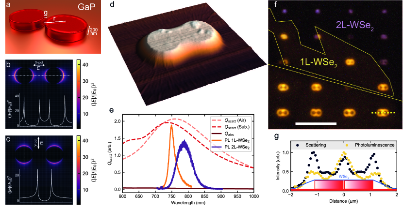
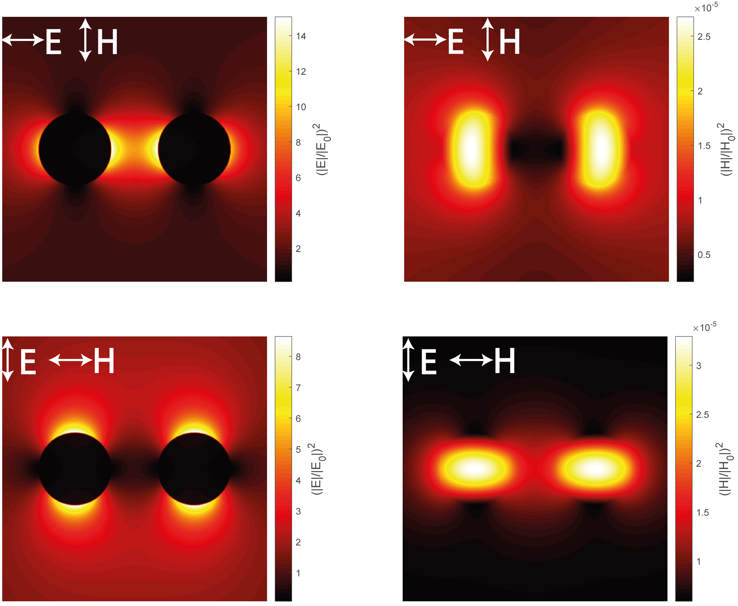
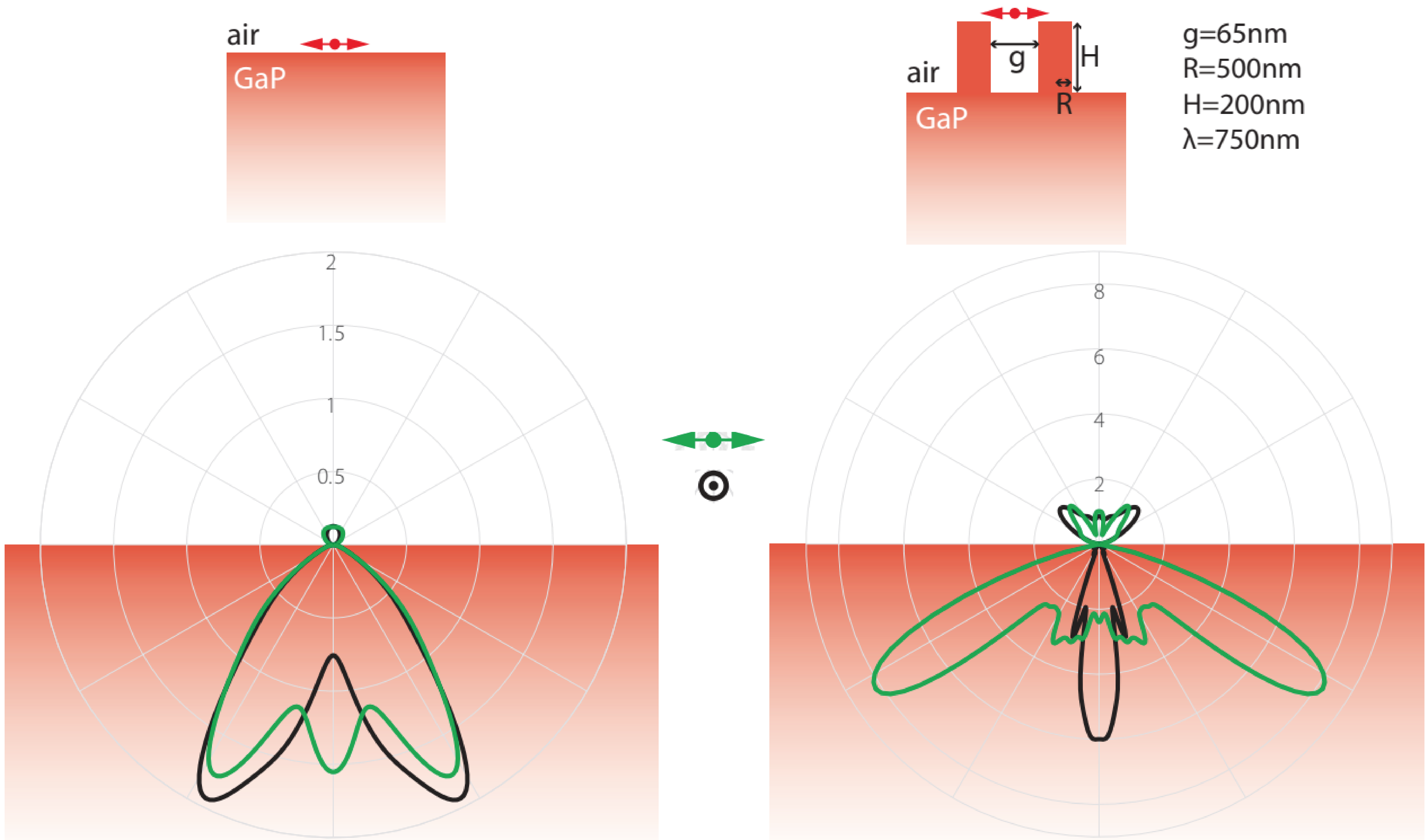
Coupling WSe2 atomic layers with dielectric nano-antennas The calculated spatial distribution of the electric field around the cylindrical double-pillar GaP nano-antennas (referred to as dimers below) is shown in Figs.1b and c. Light at a pumping wavelength of 685 nm polarised linearly along () and perpendicular () to the line connecting the centres of the pillars is used. is shown for the plane containing the top surface of the dimer, i.e. 200 nm above the planar substrate. Here and are the electric field amplitudes of the wave scattered by the pillars and the normally incident wave, respectively. The two-dimensional distribution in the plane is shown as a colour-map. In the small volume within the dimer gap an enhancement is only observed for the -polarisation Cambiasso2017a ; Regmi2016 (see further details in Supplementary Note I). The graphs shown with white lines present the variation of along the horizontal and vertical dotted lines, revealing strong maxima at the edges of the pillars. For the -polarisation, at this height of 200 nm, these maxima are stronger than the values in the gap. They are also stronger than the enhancement values at the pillar edges in the -polarisation.
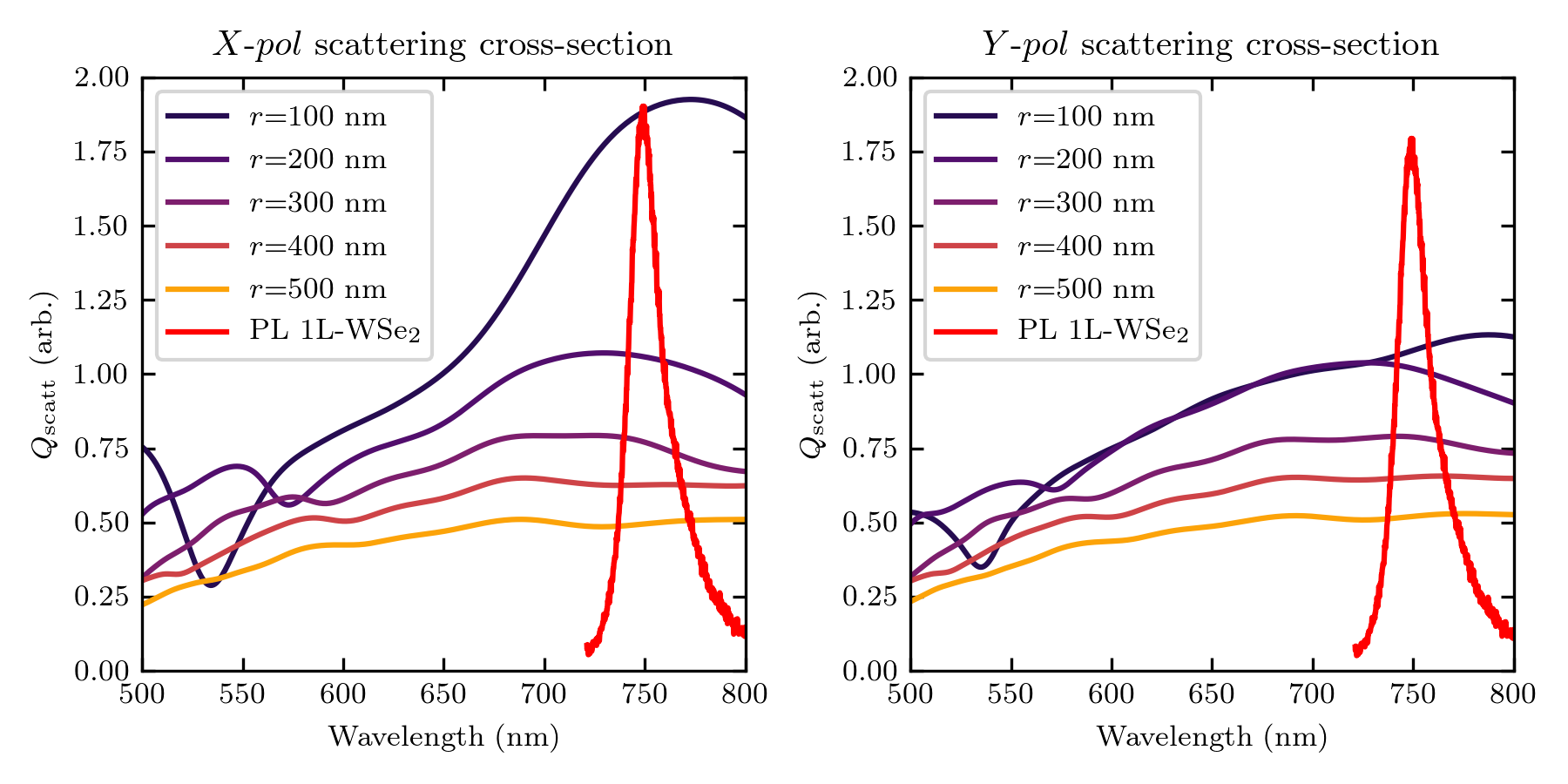
Atomic force microscopy (AFM, Fig.1d) shows that the transferred atomically thin layer of WSe2 closely follows the shape of the dimer, thus strongly overlapping with the volume of the confined optical mode. As shown in Fig.1e the spectral response of the nano-antenna is very broad, extending well into the visible and near-infra-red ranges, and fully overlapping with the PL spectra of both 1L and 2L-WSe2 (see also Supplementary Note II).
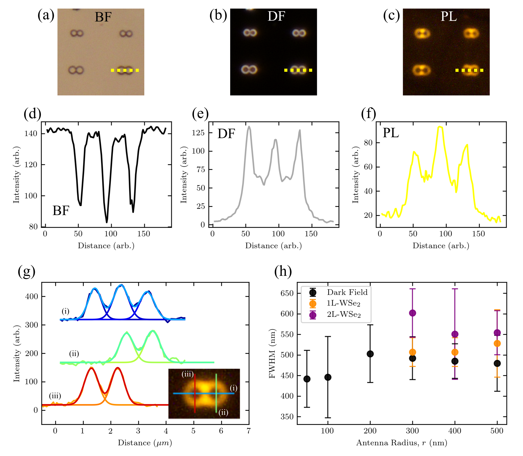
Fig.1f shows a PL image of 1L and 2L samples deposited on an array of nano-antennas and measured using an optical microscope. The image is recorded using the techniques of Ref. Alexeev2017 with unpolarised white light illuminating the sample through a short-pass filter and a long-pass filter installed in the imaging path. Bright PL replicating the shape of the dimers is visible for both 1L (yellow) and 2L (purple), whereas the PL from WSe2 on planar GaP is very weak (dark areas around the pillars). A comparison of the intensities in the PL and dark field microscopy images is shown in Fig.1g, where the intensities are measured along the dotted line shown for one of the nano-antennas in Fig.1f. The PL enhancement is observed most strongly around the edges and in the gap of the nano-antenna, where, as seen in the dark field profile, most of the light is scattered by the pillars. Further comparison of the PL, bright and dark field images is given in Supplementary Note III.
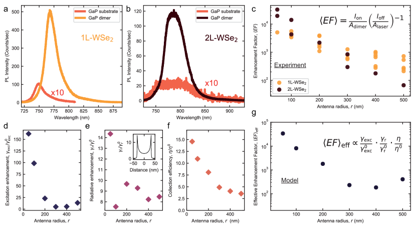
Photoluminescence enhancement factor We have additionally carried out detailed room temperature PL measurements in our micro-PL setup for 1L and 2L-WSe2 placed on GaP nano-antennas. We use a laser with wavelength 685 nm, which is below the GaP absorption edge, and is absorbed only in the WSe2 layer. Figs.2a and b show PL spectra for 1L and 2L-WSe2 coupled to GaP nano-antennas with 300 nm and 100 nm, respectively, and compare them with PL from the 2D layers placed on the planar GaP. Strong enhancement of PL intensity exceeding 50 times for WSe2 placed on nano-antennas is observed. Lower PL intensity for 2L-WSe2 is a consequence of its indirect bandgap, in contrast to the 1L-WSe2 having a direct band-gap. The effect of strain present in WSe2 placed on the nano-pillar is evident in the PL redshift for 1L and spectral modification for 2L samples.
We compare the observed PL intensity for WSe2 coupled to the nano-antennas () to that of the uncoupled WSe2 on planar GaP () by introducing the PL enhancement factor Akselrod2014 ; Wang2016c ; Cambiasso2018 ; Koenderink2017 , , defined as:
| (1) |
Here we take into account the considerable difference between the PL collection area defined by the excitation laser spot of 3.5 m diameter, and the geometrical area for a given dimer, . We expect that is larger than the actual area from where the enhanced PL is collected (mostly the edges of the pillars and the dimer gap). Thus, calculated in this way is expected to be a lower bound estimate of the observed effect.
Fig.2c shows the values extracted from the experimental data for different nano-antennas. for 1L-WSe2 exhibits an increase from 102 for the large nm pillars to nearly for nm, whereas the variation is more pronounced for the 2L samples, where changes from to . Such large values are comparable with the highest reported in plasmonic/TMDs systems Wang2016c .
As we show below, the observed enhancement is the consequence of the interaction of WSe2 with the optical mode of the nano-antenna. The extremely efficient overlap between the 2D layers and the optical mode field maxima are important for enhancing the interaction with the nano-antennas. Fig.2c shows that there is a variation of between the antennas of the same size. There are several factors that can cause this. (1) Non-uniformity of the coupling between WSe2 and the nano-antennas caused by a variety of factors such as local contamination from the polymer used for the WSe2 transfer, local deformation of WSe2, local presence of water etc. (2) Non-uniformity of the structural properties of the nano-antennas. For example, the size of the gap may vary. The quality of etching may also vary, for example producing side-walls of the pillars, which are not perfectly vertical etc.
A smaller value of for the 2L sample for the nano-antennas with the large radii is probably due to its higher rigidity compared with 1L. As the radius becomes smaller the 2L conforms more closely with the shape of the nano-antenna, and in addition the increased strain in the crystal may lead to the indirect to direct bandgap crossover Desai2014 , yielding larger values of .
Comparison of experimental data with the model In order to compare the results with our model (see Methods and Supplementary Note IV), we introduce an effective enhancement factor defined as the product of three factorsKoenderink2017 :
| (2) |
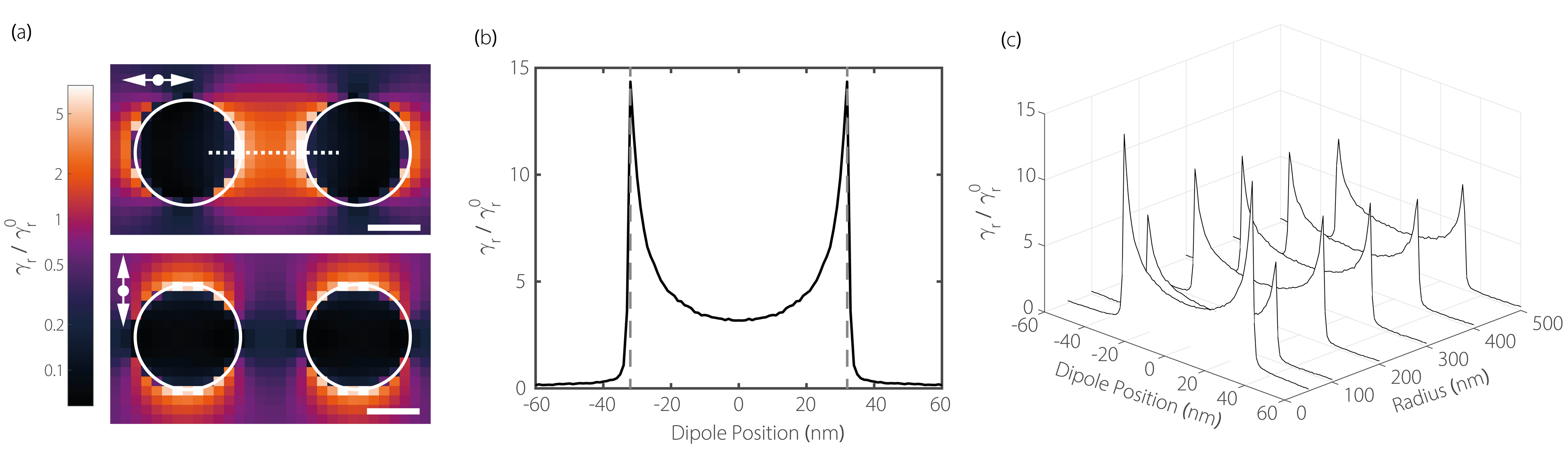
Here is the ratio of the excitation rates at a wavelength , for an emitter coupled to the antenna () and placed on the planar substrate (). Their ratio would account for the enhancement of the incident radiation leading to stronger light absorption in WSe2. , for which the spatial distribution is shown in in Figs.1b,c. We find that additional increase of the ratio arises from the reduction of for an emitter placed 0.5 nm above the planar GaP substrate compared with that for an emitter in the free space. The dependence of on the pillar radius is shown in Fig.2d for calculated for an electric dipole placed 0.5 nm above the top surface of the pillars. The dipole is placed at the edge of one of the pillars just outside the gap. As shown in the inset in Fig.2e and in Supplementary Note IV this is the position where the coupling to the optical mode of the dimer is maximized. The data in Fig.2d-f, showing the individual contributions of the different terms to the overall enhancement in Eq.2, are calculated for this position of the dipole.
The second term describes the enhancement of the quantum yield () for an emitter at a wavelength . This is achieved through the enhanced rate of spontaneous emission Cambiasso2018 described by the Purcell factor , where and are the rates of spontaneous emission for the emitter coupled to the antenna and placed on the planar GaP, respectively. In our model we consider the limit of a low quantum yield for the emitter, i.e. the non-radiative decay , which leads to . The dependence on for this term is shown in Fig.2e.
The third term describes the improved collection efficiency for WSe2 PL on top of the nano-antennas () compared to planar GaP (), as the emitted radiation is coupled to our detector using collection through numerical aperture NA=0.7 (see Supplementary Note V). The dependence on of is shown in Fig.2f.
Fig.2g shows the calculated values of the effective enhancement factor taking into account the above three mechanisms Koenderink2017 ; Cambiasso2018 (see Methods and Supplementary Note IV). The dependences of and are in a good qualitative agreement, suggesting that our model captures the main contributing factors.
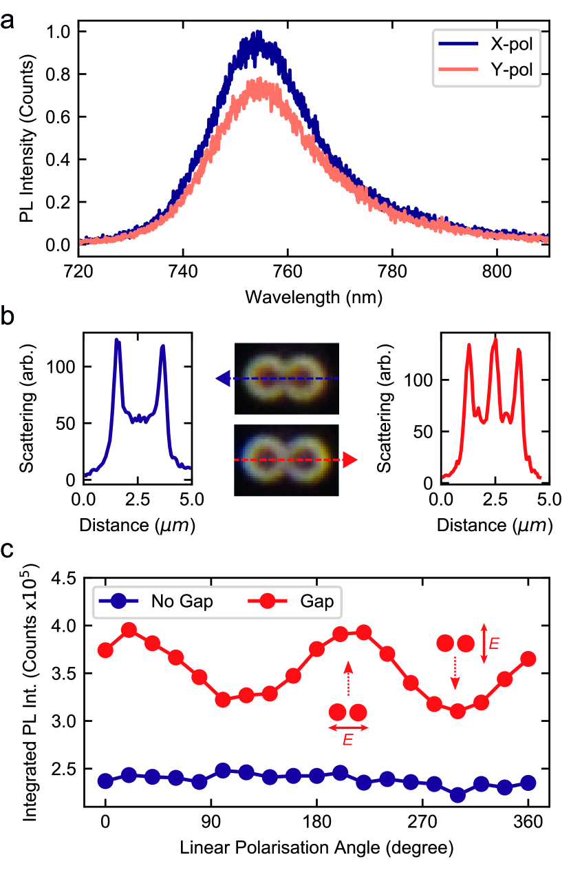
Polarisation dependent luminescence We find further evidence for the sensitivity of the WSe2 coupling to the optical mode of the dimer in polarisation resolved PL measurements. The spatial asymmetry of the dimer nano-antenna and the enhanced field in the gap between the two pillars is expected to lead to a polarisation-dependent response Regmi2016 ; Cambiasso2017a as predicted by Figs.1b,c. Such behavior is found in PL in WSe2 coupled to nano-antennas, as shown in Fig.3a-c. Fig.3a shows the case for a nano-antenna with nm and a gap nm. It is observed that PL is 20 stronger when excited with an -polarised laser compared to the -polarised excitation ( and are selected as in Figs.1b,c). A similar modulation is observed in dimers with other values of (see Supplementary Note VI). The origin of this behaviour is further revealed when considering touching pillars with no gap. Fig.3b shows the dark-field microscope images of dimers without (top) and with (bottom) a gap. The graphs in Fig.3b show the extracted scattering intensities along the line connecting the centres of the pillars, revealing the absence (left) or the presence (right) of the gap. Fig.3c shows the integrated PL intensity for WSe2 coupled to such dimers measured in a micro-PL set-up. In the dimer with a gap, the PL is modulated by 20 when varying the polarisation of excitation, exhibiting higher intensity for -polarised laser, which is due to the excitation of the optical mode in the gap between the pillars. A negligible polarisation dependence is observed in the dimer with no defined gap, emphasizing nearly equal coupling of WSe2 to the - and -polarised optical modes.
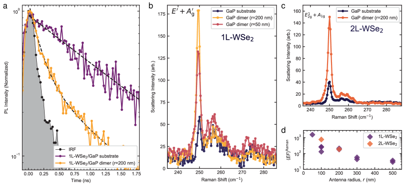
Radiative decay enhancement The theoretical interpretation in Fig.2 demonstrates that partly the PL enhancement originates from the enhanced radiative decay rate in WSe2. We have been able to demonstrate this experimentally by measuring PL dynamics in WSe2. Fig.4a shows the PL decay for a 1L-WSe2 placed on the planar GaP (purple) compared to the emission when it is coupled to a nano-antenna with nm (orange). The curves are measured using excitation with a 90 ps pulsed laser at 638 nm and detection with an avalanche photo-diode detector (see Methods). The corresponding instrument response function (IRF) is shown in Fig.4a as a gray shaded area. For these measurements, we used a low excitation density (0.2 W/cm2) to avoid non-radiative exciton-exciton annihilation, resulting in fast PL decay Mouri2014 ; Wang2017 . For low pumping powers, single exponential decay is usually observed, reflecting the radiative recombination dynamics of the thermalised exciton population Robert2016 ; Godde2016 . Such behaviour is observed in Fig.4a for the 1L-WSe2 on the planar GaP, which shows a single-exponential PL decay with a lifetime ns. The PL decay measured for WSe2 coupled to a dimer is dominated by a fast component with a lifetime ns. This is very similar to the fast component in the instrument response function (IRF) of ns. We thus conclude that the measured ns is a resolution-limited value. We interpret the shortening of the PL lifetime as a consequence of the Purcell enhancement of the radiative rate. A conservative lower-bound estimate of the Purcell enhancement factor is therefore 6. This is in a good agreement with the theoretical predictions, for which we should take into account the spatial variation of the Purcell enhancement in the WSe2 coupled to the mode. Note that Fig.2e only shows the values obtained for the optimum location of the dipole where the enhancement is maximised (see further details in Supplementary Note IV).
Surface enhanced Raman scattering Further evidence for the efficient interaction of WSe2 with the nano-antennas is obtained from the observation of the enhanced Raman scattering response. This effect, typically observed for nano-structured metals Maier and dielectric nano-particles Alessandri2016 , is related to the surface localization of the electromagnetic field. Both 1L and 2L-WSe2 Raman spectra excited with a laser at 532 nm show a pronounced peak at 250 cm-1 composed of two degenerate modes, the in-plane for 1L and for 2L WSe2, and out-of-plane for 1L and for 2L WSe2 Tonndorf2005 . This is shown in Figs.4b and c for 1L and 2L samples, respectively. Figs.4b,c further compare Raman spectra measured for WSe2 on the planar GaP with the spectra collected on nano-antennas, and show a notable enhancement of the signal. While the overall Raman signal decreases with decreasing , its relative strength per unit nano-antenna area is strongly enhanced. In analogy with the PL data, we define the Raman experimental enhancement factor, (see Methods). The obtained values increase when reducing the antenna radius, as for the PL enhancement, with values exceeding 103 for 50 nm (Fig.4d). The observed Raman intensity enhancement is explained by the enhancement of the laser and the scattered light fields and a more efficient collection of the signal (see Eq.2).
Discussion
The reported enhancement in the PL emission and Raman signal intensities, and shortening of the radiative lifetime in 2D WSe2 coupled to GaP nano-antennas, shows that nano-structured high-index dielectrics can be an efficient platform to engineer light-matter coupling on the nano-scale. Importantly, we show that the coupling to nano-antennas can be used to strongly enhance the quantum yield in TMDs via the enhancement of the radiative decay rate, emphasizing the potential of this approach for light-emitting devices applications. The PL enhancements, which we report are of the order or exceed those recently reported in TMDs coupled to metallic plasmonic nano-antennas, showing the viability of our approach in a broader nano-photonics context. Our approach could be further extended to arrays of dielectric nano-structures, or meta-surfaces, an emerging field of nano-photonicsJahani2016 , and to the use of van der Waals nano-photonics structures made from multilayer TMDsVerre2018 , with potential in a wide range of applications, such as quantum optics, photovoltaics and imaging. The approaches for realisation of the Purcell effect in loss-less dielectrics demonstrated here will also be used in the field of strain-induced single photon emitters Palacios-Berraquero2016c ; Branny2016 for applications exploiting quantum light generation.
METHODS
Sample fabrication
GaP nano-antennas arrays are fabricated with the top-down lithographic process following the procedure in Ref.Cambiasso2017a . The fabricated pillars are 200 nm high and have radi of r = 50 nm, 100 nm, 200 nm, 300 nm, 400 nm, 500 nm. Monolayers and bilayers of WSe2 were mechanically exfoliated from a bulk crystal (HQGraphene) onto a poly-methyldisyoloxane (PDMS) polymer stamp. The thin layers are identified via the PL imaging technique described in this work in Fig.1 and Ref.Alexeev2017 . The stamp was then used for an all-dry transfer of the exfoliated materials on top of the GaP nano-antenna array, in an home-built transfer setup following RefCastellanos-Gomez2014a .
Photoluminescence imaging
The PL imaging technique Alexeev2017 used in Fig.1 is obtained in a modified commercial bright-field microscope (LV150N Nikon). The white light source is used both for imaging the sample and as the PL excitation source. To excite the sample a 550 nm short-pass filter is placed in the illumination beam path to remove the near-IR part of the emission spectrum. The white light is then directed in a large numerical aperture objective (Nikon x100 NA=0.9) and collected with the same objective. The PL signal produced by the TMDs is isolated with a 600 nm long-pass filter before reaching the colour microscope camera (DS-Vi1, Nikon) used to image the sample.
Photoluminescence spectroscopy
All PL spectra are acquired at room temperature in a micro-PL set-up with samples placed in vacuum. A 685 nm diode laser coupled to a single mode fibre is used as the excitation source. After passing through a 700 nm short-pass filter, the laser is focussed onto the sample through an infinity corrected objective (Mitutoyo 100x NA=0.7). For the data reported in Fig.2, the average power entering the objective is 30 for monolayer PL and 120 for bilayer PL. The resulting laser spot has a radius of m which is large enough to illuminate entire individual dimers, and kept constant for a uniform excitation of all the different nano-antennas sizes when determining the reported enhancement factor in Eqn.1. The dimers are separated by 10 m, which allows optical measurement of an individual dimer. The emitted light is collected by the same objective and filtered with a 700 nm long pass filter before coupling into a spectrometer (Princeton Instruments SP2750) and detection with a high-sensitivity liquid nitrogen cooled charge-coupled device (CCD, Princeton Instruments PyLoN). For polarisation measurements, a Glan-Thompson linear polariser, followed by a half-wave plate mounted onto a motorized rotation stage, are inserted in the excitation path in order to control the linear polarisation angle of the laser source. No polarisation optics is used in the collection path.
Time-resolved spectroscopy
PL decay of planar WSe2 is measured by coupling light filtered by a spectrometer (4 nm bandwidth) into a multi-mode fibre directing light to an avalanche photodiode (APD, ID100-MMF50) with time-resolution of 40 ps. The signal from the APD is read using a photon counting card (SPC-130). A 90 ps pulsed diode laser (PicoQuant LDH) with wavelength 638 nm is used as the excitation source at a repetition rate of 80 MHz. Overall, the instrument response function (IRF) has a full width at half maximum of 200 ps. The PL decay curves are fitted with single and bi-exponential decay functions of the form .
Raman spectroscopy
Raman spectra are collected at room temperature in a micro-Raman set-up with samples placed in vacuum. A single mode 532 nm laser (Cobolt 04-01) is used, focussed on the sample through an infinity corrected objective (Mitutoyo 50x NA=0.55) with an average power of 200 before entering the objective. Background laser light is suppressed using three Optigrate Bragg filters, which allow Raman signal to be measured by the same spectrometer/CCD system as for PL spectroscopy. The Raman signals are analysed by fitting the two WSe2 Raman peaks with Gaussian functions, following background subtraction. The 250 cm-1 peak intensities extracted in this way are used to calculate the Raman enhancement factor in Eq.3 given below. In this equation is the Raman intensity for WSe2 coupled to a dimer and is for the reference WSe2 on the planar GaP. We determined experimentally that m2 in the micro-Raman set-up.
| (3) |
Simulations
The effective enhancement factor contributions are calculated with a finite-difference time-domain (FDTD) method using Lumerical FDTD solutions software. The near-field distribution is obtained by illuminating the structure with a plane wave, polarised along or perpendicular the dimer axis (the line connecting the centres of the pillars) and incident on the dimer perpendicular to the substrate from the vacuum side. The Purcell enhancement is calculated by exciting the structure with an oscillating electric dipole placed at different positions along the dimer axis at a vertical position 0.5 nm from the top surface of the GaP pillars, and compared with a dipole placed 0.5 nm above the planar surface of the GaP substrate. To model the photoluminescence in WSe2 originating from the in-plane excitons, the dipole is placed parallel to the substrate surface. The dipole oscillates along the line connecting the centres of the pillars in order to couple efficiently to the gap mode. The Purcell enhancement is calculated as the decay rate of an emitter coupled to the GaP antenna, divided by the decay rate of the same electric dipole emitter on the planar GaP substrate as described above. The decay rate enhancement corresponds to the enhancement of the rate of energy dissipation . The collection efficiency is calculated by exciting the structure with an electric dipole, as above, and integrating the radiation pattern within the numerical aperture of the objective used in the experiments (NA=0.7). The refractive index used for GaP is n=3.2.
Competing interests
The authors declare no competing interests
Data availability
The data that support the findings of this study are available from the corresponding author upon reasonable request.
References
- (1) Mak, K. F. & Shan, J. Photonics and optoelectronics of 2D semiconductor transition metal dichalcogenides. Nat. Photonics 10, 216–226 (2016).
- (2) Wang, G. et al. Colloquium : Excitons in atomically thin transition metal dichalcogenides. Rev. Mod. Phys. 90, 021001 (2018).
- (3) Mueller, T. & Malic, E. Exciton physics and device application of two-dimensional transition metal dichalcogenide semiconductors. npj 2D Mater. Appl. 2, 29 (2018).
- (4) Wu, S. et al. Monolayer semiconductor nanocavity lasers with ultralow thresholds. Nature 520, 69–72 (2015).
- (5) Zhang, L., Gogna, R., Burg, W., Tutuc, E. & Deng, H. Photonic-crystal exciton-polaritons in monolayer semiconductors. Nat. Commun. 9, 1–8 (2018).
- (6) Li, Y. et al. Room-temperature continuous-wave lasing from monolayer molybdenum ditelluride integrated with a silicon nanobeam cavity. Nat. Nanotechnol. 12, 987–992 (2017).
- (7) Salehzadeh, O., Djavid, M., Tran, N. H., Shih, I. & Mi, Z. Optically Pumped Two-Dimensional MoS2 Lasers Operating at Room-Temperature. Nano Lett. 15, 5302–5306 (2015).
- (8) Geim, A. K. & Grigorieva, I. V. Van der Waals heterostructures. Nature 499, 419–425 (2013).
- (9) Liu, X. et al. Strong light-matter coupling in two-dimensional atomic crystals.. Nat. Photon. 9, 30 (2015).
- (10) Dufferwiel, S. et al. Exciton-polaritons in van der Waals heterostructures embedded in tunable microcavities. Nat. Commun. 6, 8579 (2015).
- (11) Sidler, M. et al. Fermi polaron-polaritons in charge-tunable atomically thin semiconductors. Nat. Phys. 13, 255–261 (2016).
- (12) Schneider, C. et al. Two-dimensional semiconductors in the regime of strong light-matter coupling.. Nat. Commun. 9, 2695 (2018).
- (13) Amani, M. et al. Near-unity photoluminescence quantum yield in MoS2. Science 350, 1065 (2015).
- (14) Maier, S. A. Plasmonics: Fundamentals and Applications. (Springer US, New York, NY, 2007).
- (15) Koenderink, A. F. Single-Photon Nanoantennas. ACS Photonics 4, 710 (2017).
- (16) Kern, J. et al. Nanoantenna-Enhanced Light-Matter Interaction in Atomically Thin WS2. ACS Photonics 2, 1260 (2015).
- (17) Lee, B. et al. Fano Resonance and Spectrally Modified Photoluminescence Enhancement in Monolayer MoS2 Integrated with Plasmonic Nanoantenna Array. Nano Lett. 15, 3646 (2015).
- (18) Butun, S. et al. Enhanced Light Emission from Large-Area Monolayer MoS2 Using Plasmonic Nanodisc Arrays. Nano Lett. 15, 2700 (2015).
- (19) Wang, Z. et al. Giant photoluminescence enhancement in tungsten-diselenide-gold plasmonic hybrid structures. Nat. Commun. 7, 11283 (2016).
- (20) Tahersima, M. H. et al. Testbeds for Transition Metal Dichalcogenide Photonics - Efficacy of Light Emission Enhancement in Monomer vs Dimer Nanoscale Antennae. ACS Photonics 4, 1713 (2017).
- (21) Cheng, F. et al. Enhanced Photoluminescence of Monolayer WS2 on Ag Films and NanowireWSFilm Composites. ACS Photonics 4, 1421 (2017).
- (22) Kleemann, M.-E. et al. Strong-coupling of WSe2 in ultra-compact plasmonic nanocavities at room temperature. Nat. Commun. 8, 1296 (2017).
- (23) Wen, J. et al. Room-Temperature Strong Light–Matter Interaction with Active Control in Single Plasmonic Nanorod Coupled with Two-Dimensional Atomic Crystals. Nano Lett. 17, 4689 (2017).
- (24) Cuadra, J. et al. Observation of Tunable Charged Exciton Polaritons in Hybrid Monolayer WS2-Plasmonic Nanoantenna System. Nano Lett. 18, 1777 (2018).
- (25) Park, K.-D. D., Jiang, T., Clark, G., Xu, X. & Raschke, M. B. Radiative control of dark excitons at room temperature by nano-optical antenna-tip Purcell effect. Nat. Nanotechnol. 13, 1–6 (2017).
- (26) Luo, Y. et al. Deterministic coupling of site-controlled quantum emitters in monolayer WSe2 to plasmonic nanocavities. Nat. Nanotechnol. 13, 1137–1142 (2018).
- (27) Cai, T. et al. Radiative Enhancement of Single Quantum Emitters in WSe2 Monolayers Using Site-Controlled Metallic Nanopillars. ACS Photonics 5, 3466 (2018).
- (28) Caldarola, M. et al. Non-plasmonic nanoantennas for surface enhanced spectroscopies with ultra-low heat conversion. Nat. Commun. 6, 7915 (2015).
- (29) Krasnok, A., Lepeshov, S. & Alú, A. Nanophotonics with 2D transition metal dichalcogenides. Opt. Express 26, 15972 (2018).
- (30) Kuznetsov, A. I., Miroshnichenko, A. E., Brongersma, M. L., Kivshar, Y. S. & Luk’yanchuk, B. Optically resonant dielectric nanostructures. Science 354, 2472 (2016).
- (31) Mignuzzi, S. et al. Nanoscale Design of the Local Density of Optical States. Nano Lett. 19, 1613–1617 (2019).
- (32) Cambiasso, J. et al. Bridging the Gap between Dielectric Nanophotonics and the Visible Regime with Effectively Lossless Gallium Phosphide Antennas. Nano Lett. 17, 1219–1225 (2017).
- (33) Cihan, A. F., Curto, A. G., Raza, S., Kik, P. G. & Brongersma, M. L. Silicon Mie resonators for highly directional light emission from monolayer MoS2. Nat. Photonics 12, 284–290 (2018).
- (34) Lepeshov, S. et al. Tunable Resonance Coupling in Single Si Nanoparticle-Monolayer WS2 Structures. ACS Appl. Mater. Interfaces 10, 16690–16697 (2018). eprint 1710.09949.
- (35) Verre, R. et al. Transition metal dichalcogenide nanodisks as high-index dielectric Mie nanoresonators. Nat. Nanotechnol. (2019).
- (36) Jahani, S. & Jacob, Z. All-dielectric metamaterials. Nat. Nanotechnol. 11, 23–36 (2016).
- (37) Regmi, R. et al. All-Dielectric Silicon Nanogap Antennas To Enhance the Fluorescence of Single Molecules. Nano Lett. 16, 5143–5151 (2016).
- (38) Alexeev, E. M. et al. Imaging of Interlayer Coupling in van der Waals Heterostructures Using a Bright-Field Optical Microscope. Nano Lett. 17, 5342–5349 (2017).
- (39) Akselrod, G. M. et al. Probing the mechanisms of large Purcell enhancement in plasmonic nanoantennas. Nat. Photonics 8, 835–840 (2014).
- (40) Cambiasso, J., König, M., Cortés, E., Schlücker, S. & Maier, S. A. Surface-Enhanced Spectroscopies of a Molecular Monolayer in an All-Dielectric Nanoantenna. ACS Photonics 5, 1546–1557 (2018).
- (41) Desai, S. B. et al. Strain-Induced Indirect to Direct Bandgap Transition in Multilayer WSe2. Nano Lett. 14, 4592–4597 (2014).
- (42) Mouri, S. et al. Nonlinear photoluminescence in atomically thin layered WSe2 arising from diffusion-assisted exciton-exciton annihilation. Phys. Rev. B 90, 155449 (2014).
- (43) Robert, C. et al. Exciton radiative lifetime in transition metal dichalcogenide monolayers. Phys. Rev. B 93, 205423 (2016).
- (44) Godde, T. et al. Exciton and trion dynamics in atomically thin MoSe2 and WSe2: Effect of localization. Phys. Rev. B 94, 165301 (2016).
- (45) Alessandri, I. & Lombardi, J. R. Enhanced Raman Scattering with Dielectrics. Chem. Rev. 116, 14921–14981 (2016).
- (46) Tonndorf, P. et al. Photoluminescence emission and Raman response of monolayer MoS2, MoSe2, and WSe2. Opt. Express 21, 4908 (2013).
- (47) Palacios-Berraquero, C. et al. Large-scale quantum-emitter arrays in atomically thin semiconductors. Nat. Commun. 8, 15093 (2017).
- (48) Branny, A., Kumar, S., Proux, R. & Gerardot, B. D. Deterministic strain-induced arrays of quantum emitters in a two-dimensional semiconductor. Nat. Commun. 8, 15053 (2017).
- (49) Castellanos-Gomez, A. et al. Deterministic transfer of two-dimensional materials by all-dry viscoelastic stamping. 2D Mater. 1, 011002 (2014).
Acknowledgements
A. I. T. thank the financial support of the European Graphene Flagship Project under grant agreements 696656 and 785219, and EPSRC grant EP/P026850/1. L. S. and A. I. T. acknowledge support from the European Union’s Horizon 2020 research and innovation programme under ITN Spin-NANO Marie Sklodowska-Curie grant agreement no. 676108. P. G. Z. and A. I. T. acknowledge support from the European Union’s Horizon 2020 research and innovation programme under ITN 4PHOTON Marie Sklodowska-Curie grant agreement no. 721394. S. M., S. A. M., and R. S. acknowledge funding by EPSRC (EP/P033369 and EP/M013812). S. A. M. acknowledges the Lee-Lucas Chair in Physics and the DFG Cluster of Excellence Nanoscience Initiative Munich (NIM). M. A. and M. B. thank the DFG in the frame of TRR 142 for support.
Author contributions
L. S. and P. G. Z. fabricated WSe2 layers and transferred them on the GaP nano-antennas. L. S., P. G. Z. and A. G. carried out microscopy and cw optical measurements on WSe2. L. S., D. S. and M. A. carried out time-resolved PL measurements. J. C. fabricated GaP nano-antennas. S. M., J. C. and R. S. carried out simulations for GaP nano-antennas. L. S., D. S., M. A., P. G. Z., A. G., M. B. and A. I. T. analysed optical spectroscopy data. M. B., S. A. M., R. S. and A. I. T. managed various aspects of the project. L. S. and A. I. T. wrote the manuscript with contributions from all co-authors. L. S., A. I. T., S. A. M., R. S. conceived the idea of the experiment. A. I. T. oversaw the whole project.
Supplementary Note I: Spatial distributions of electric and magnetic fields produced by gallium phosphide dimer nano-antennas
Supplementary Note II: Light scattering by gallium phosphide dimer nano-antennas
The scattering cross section of a nano-particle can be defined as the ratio between the power radiated by the nano-antenna over the incident powerNovotny2006 . The corresponding absorption efficiency can be estimated as , where is the extinction cross section. The relative efficiency, , is calculated as the ratio between the relative cross section divided by the geometric area of the dimer, given by , where is the nano-pillar radius. Fig.6 shows the calculated scattering efficiency for different radii GaP dimer nano-antennas, and for X and Y polarisation geometries. As shown, the scattering response fully overlaps with the PL emission profile of monolayer WSe2.
Supplementary Note III: Comparison of different imaging techniques for WSe2 coupled to nano-antennas
Supplementary Note IV: Calculation of the Purcell enhancement produced by the gallium phosphide nano-antennas
The Purcell enhancement is calculated as the decay rate of an emitter coupled to the GaP nano-antenna, normalised with the decay rate of an emitter on a planar GaP substrate. The decay rate enhancement corresponds to the enhancement of the rate of energy dissipation , which we calculate with a finite-difference time-domain (FDTD) method (Lumerical software). We have calculated the power radiated by an electric dipole at 0.5 nm distance from the top surface of the GaP pillars, for different positions over the dimer, and compared that to the power radiated by the same dipole placed 0.5 nm above the surface of the planar substrate. In order to model our experimental system where photoluminescence in WSe2 originates from the in-plane excitons, the dipole is placed parallel to the surface of the pillars or the substrate, polarised along the direction parallel or perpendicular to the dimer axis. Fig. 8a plots the 2D maps of the Purcell enhancement around the dimer, for the two dipole orientations as indicated by the white arrow. In Fig. 8b a dependence of on the position in the dimer gap is shown for a dimer with =50 nm. Strong maxima are observed close to the edges of the pillars (marked with dotted lines in Fig. 8a) with the Purcell enhancement values reaching 15. As Fig.8c shows, the maximum Purcell enhancement values increase as is varied from 500 to 50 nm, while their positions remain the same in the proximity of the pillar edges.
Supplementary Note V: Calculated emission pattern for gallium phosphide nano-antennas in comparison with planar gallium phosphide
Supplementary Note VI: Polarisation-resolved PL of WSe2 coupled to nano-antennas
References
- (1) Novotny, L. & Hecht, B. Principles of Nano-Optics (Cambridge University Press, Cambridge, 2006).