Plasmonic lenses for tunable ultrafast electron emitters at the nanoscale
Abstract
Simultaneous spatio-temporal confinement of energetic electron pulses to femtosecond and nanometer scales is a topic of great interest in the scientific community, given the potential impact of such development on a wide spectrum of scientific and industrial applications. For example, in ultrafast electron scattering, nanoscale probes would enable accurate maps of structural dynamics in materials with nanoscale heterogeneity, thereby understanding the role of boundaries and defects on macroscopic properties. On the other hand, advances in this field are mostly limited by the electron source brightness and size. We present the design, fabrication, and optical characterization of bullseye plasmonic lenses for next-generation ultrafast electron sources. Using electromagnetic simulations, we examine how the interplay between light-plasmon coupling, plasmon propagation, dispersion, and resonance governs the properties of the photoemitted electron pulse. We also illustrate how the pulse duration and strength can be tuned by geometric design, and predict sub-10 fs pulses with nanoscale diameter can be achieved. We then fabricated lenses in gold films and characterized their plasmonic properties with cathodoluminescence spectromicroscopy, demonstrating suitable plasmonic behavior for ultrafast, nanoscale photoemission.
I Introduction
Ultrafast electron sources have been extensively used as tools for scientific discovery over the past two decades. Such sources can now reliably produce electron pulses with femtosecond duration, which can be used as probes for dynamic microscopy and scattering measurements. Ultrafast electron-based measurements have provided insight into mechanisms of structural phase transitions in condensed matter Siwick et al. (2003); Morrison et al. (2014); Eichberger et al. (2010) as well as chemical reactions and photochemistry in gases and molecular solids Zewail (2006); Gao et al. (2013). Even so, ultrafast electron experimentation is still limited by the source brightness, defined as the number density of electrons in transverse phase space [i.e. per unit solid angle and unit area, also called four-dimensional (4D) emittance] Rhee (1992), and setting a limit to beam relative coherence and focusability Carbone et al. (2012). Spatio-temporal mapping with both nanoscale spatial and femtosecond temporal resolution is rarely utilized Feist et al. (2018); da Silva et al. (2018); Yurtsever et al. (2012), and typically requires a combination of high contrast signals, several hour acquisition times, and limited sampling. Electron-based mapping of dynamics with increased throughput and detail may provide key insights into how microstructure and defects locally influence phase transformation, carrier generation and recombination, phonon and plasmon propagation, and much more.
In effort to increase brightness, researchers have developed radio-frequency-based electron guns (rf guns) capable of sustaining large electric field amplitudes at extraction and during acceleration. By providing an order of magnitude higher accelerating field (100 MV/m) than direct-current electron guns, the extracted peak current can be increased by orders of magnitude, from the A-range typical of electron microscopes to several A, while generating relativistic electron pulses with sub-10-fs duration Maxson et al. (2017); Zhao et al. (2018). Yet, tip emitters typically used in electron microscopes are not easily used in rf guns since under such high fields, they have limited lifetime and tend to emit dark electrons via field emission Huang et al. (2015), which are not synchronous with the laser pulse and add background to the experiment. Instead, flat cathodes are often used, which have much larger emission areas in the range of tens of m or larger, ultimately limited by the incident laser spot size. Considering conservation of the beam emittance, larger source size in turn produces proportionally larger spot size for a given angular spread, thereby limiting the minimum useful spot size for applications.
Recently, nanostructured cathode surfaces have been demonstrated that couple the incident laser to resonant surface plasmon modes, which concentrate and enhance the optical-field intensity in localized areas of the surface. For example, nanogrooves designed to produce an in-groove surface plasmon resonance were patterned into gold-coated cathodes and were found to increase the photocurrent yield by 6 orders of magnitude over bare gold through multiphoton photoemission Polyakov et al. (2013). Nanohole arrays designed to have a grating resonance have also been demonstrated in copper cathodes, increasing photocurrent yield 120 times over bare copper Li et al. (2013). This approach to improving the emission characteristics is compatible with high accelerating fields. However, the photoemitted beams in these cases still had limited quality Li et al. (2013): The optical fields were concentrated at edges, inducing emittance growth similar to the effect of surface roughness Lau (1987). Also, their temporal response was not studied in detail, and may be limited by the cavity-resonance damping time. In addition, the emission is still dispersed over several micron areas in these initial demonstrations.
In this work, we propose and investigate the potential of bullseye plasmonic lenses for ultrafast, nanoscale photoemitters. Such structures concentrate optical fields to a single, central spot on a flat surface Steele et al. (2006); Chen et al. (2009), potentially providing aberration-free electron emission and enabling the use of nanoscale photo-triggered emitters in high-field environments. We first show electromagnetic simulations to demonstrate how to control the spatiotemporal characteristics of the optical fields and the corresponding photoemission by geometric design. Then, we demonstrate fabrication of actual bullseye lenses in gold films by two methods and characterize their plasmonic behavior using cathodoluminescence spectromicroscopy. We show that spatial and spectral plasmonic characteristics are like predicted in simulation, supporting that ultrafast nano-emission can be achieved. Altogether, the results support the potential for bullseye lenses as high brightness electron sources and establish a new research direction in the field of plasmon-enhanced ultrafast electron nano-emission.
II Plasmonic lens design and electromagnetic simulations
II.1 Lens principle and parameters
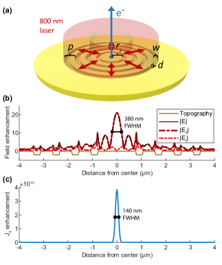
The system under study is a nanopatterned photocathode excited by ultrafast laser pulses with an 800 nm center wavelength. The pattern consists of equally-spaced, concentric annular grooves forming a bullseye plasmonic lens. The geometry is defined by the five parameters illustrated in Figure 1a: The number of rings , grating period , groove width , groove depth , and center plateau radius . Such gratings couple the component of incident light with electric field perpendicular to the grooves into surface plasmon polaritons (SPPs). A radially polarized laser at normal incidence is used so that the electric field direction is always perpendicular to the grooves and the launched SPPs are in phase. These SPPs then propagate and interfere to give maximum field enhancement at the structure center.
We use gold as the plasmonic material, enabling four-photon photoemission at 800 nm wavelength. Gold is oxidation resistant and provides effective photoemission surfaces; in fact, four-photon photoemission from gold cathodes patterned with linear gratings has been demonstrated Polyakov et al. (2013). Gold also provides long SPP propagation lengths in the red and near-infrared range: 10-15 m in as-deposited polycrystalline films Kolomenski et al. (2009); Kuttge et al. (2008) and greater than 60 m in template-stripped and single-crystal gold films McPeak et al. (2015); Olmon et al. (2012); Kuttge et al. (2008).
II.2 Nanoscale field enhancement and photoemission
We first simulate the electromagnetic fields for a lens under continuous-wave (cw) illumination to study their spatial distribution and the expected emission spot size. An 800-nm wavelength laser is focused at the surface using a numerical aperture (NA) of 0.07, giving a donut-shaped in-plane intensity with peak-to-peak diameter of 4.5 m. The lens has 4 rings with period of 783 nm, which is the corresponding SPP wavelength in gold. This aims to satisfy momentum conservation between the normal incidence photons and the SPPs as given by the grating equation Raether (1988):
| (1) |
Here, and are the in-plane wave vectors of the SPP and incident photon, respectively, while g is the grating vector and n is an integer. We set to be 783 nm to coincide with antinodes of the two-dimensional (2D) standing wave formed by the interfering SPPs. This causes reflections from the edge to resonate, further increasing field enhancement. With these parameters fixed, we then performed a series of finite-difference time-domain (FDTD) simulations in Lumerical Lumerical to optimize the depth and width of the rings for maximum field enhancement at the center. The optimum is found for = 90 nm and = 270 nm.
The electric field magnitude profiles for the optimized structure are shown in Figure 1b. The field enhancement relative to the peak field of the incident laser is maximized at the center (21.0). Also, the lateral electric field is zero at the center and remains small relative to the normal field within the four-photon photoemission peak shown in Figure 1c.
The anticipated four-photon photocurrent density Bechtel et al. (1977); the photocurrent density enhancement is shown in Figure 1b. Remarkably, the enhancement at the center is . Also, using multiphoton photoemission practically eliminates contributions from the side lobes and edges of the structure, creating a single, tightly focused emission spot with full width at half maximum (FWHM) of 140 nm in the flat center plateau.
II.3 Ultrafast temporal response
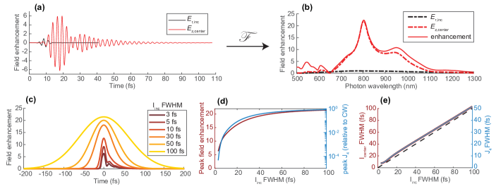
To study the emitter’s temporal response and how it depends on the lens geometry, we performed impulse-response FDTD simulations. Using incident laser pulses with 3-fs FWHM duration, we simulate the time-resolved electric field at the structure center, . The spectral response in the linear intensity regime is described by the complex transfer function T(), obtained from the Fourier transforms of the time-dependent incident and enhanced fieldsLaughton and Warne (2003):
| (2) |
The frequency-dependent field enhancement is then given by . We also use eq. 2 to compute the temporal response for Gaussian incident pulses of varying duration.
We first study the four-ring bullseye lens optimized above (see Figure 1). The simulated incident and enhanced electric fields over time are shown in Figure 2a. Notably, the plasmonic field is stronger than the incident laser field, but lasts more than 10 fs longer. In the next section, we will show that some of this broadening is due to the delay in arrival of plasmons generated from outer rings relative to inner rings. This leads to a spectral response with finite bandwidth, shown in Figure 2b as a function of incident photon wavelength. There is a strong peak at 800 nm, which we attribute to a surface plasmon resonance in the center plateau. The grooves in this structure are deep enough to disturb SPP propagation and modify their dispersion, leading to additional peaks and valleys in the response (see Figure 4). Additional peaks have been observed experimentally in transmission spectra of plasmonic lenses with a central aperture Thio et al. (2001) and computational work finds significant dispersion modification in deep gratings, such as opening of plasmonic bandgaps Hooper and Sambles (2002).
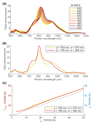
Effects on the response shape for varying incident pulse length ( FWHM) are shown in Figure 2c. Longer pulses generate a Gaussian response with peak field enhancement identical to that for cw illumination. On the other hand, for pulse lengths of tens of femtoseconds, there is substantial temporal broadening and the plasmonic field amplitude is reduced. These effects on the response strength and duration are quantified in Figure 2d-e. We note that the FWHM durations in Figure 2e are set by the main peak in the temporal envelope, while the tails are suppressed due to the scaling of four-photon photoemission with the intensity ( Bechtel et al. (1977). As a result, the response duration is mostly linear with the input pulse duration, always about 3.5 fs longer due to the propagation delay between rings. For few-femtosecond pulse lengths, there are deviations from linearity which may be related to beating and envelope asymmetry. Still, this lens is predicted to be capable of producing sub-10 fs photoelectron pulses.
II.4 Tuning the response by geometric design
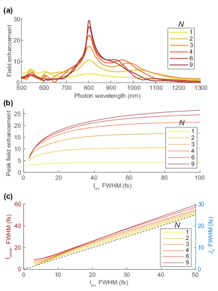
We now present a series of impulse-response simulations while varying geometric parameters to clarify design rules for ultrafast photoemission applications. We first vary the number of rings, , obtaining the simulated spectral response shown in Figure 3a. For = 1, the bandwidth extends over the entire wavelength range studied, and there is a plasmonic resonance peak at 800 nm. Adding more rings increases the field enhancement by coupling more light, but it shrinks the bandwidth by increasing the SPP propagation distance, and hence delay time, between inner and outer rings. This generally increases the peak field enhancement for varying incident pulse length shown in Figure 3b while increasing the response duration as shown in Figure 3c. For few-femtosecond pulses, however, there is a limit to the number of added rings that increase field enhancement, beyond which the delay time between inner and outer plasmons is too long for them to overlap. In this limit, adding additional rings only increases the pulse duration without increasing field enhancement, shown in Figure 3b-c at the shortest pulse durations.
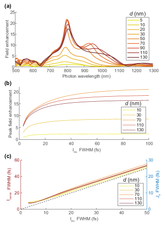
We then vary the depth of the grooves, , obtaining the spectral response shown in Figure 4a. As increases, the field enhancement increases, saturates, and eventually decreases. While deeper grooves couple more incident photons to SPPs, they also inhibit SPP propagation to the center, leading to an optimal depth that maximizes field enhancement. The resonance peak at 800 nm emerges and grows with increasing as reflectivity of plasmons from the grooves increases. Other peaks and valleys also emerge, suggesting the deeper grooves are disturbing plasmon propagation and modifying their dispersion and interference. The peak field enhancement for varying incident pulse length scales similarly with as shown in Figure 4b. Again for few-femtosecond pulses, plasmons from the outer rings cannot reach those from the inner rings and so the field enhancement is reduced. There is also a noticeable effect of on the temporal response duration as shown in Figure 4c. For longer pulses, the duration seems to scale with the strength of the resonance contribution, which would extend the plasmonic field duration. Overall, has less of an effect on the pulse duration than .
Next, we vary the ring width, , computing the transfer functions shown in Figure 5a. Maximal field enhancement is achieved for = 360 nm, close to half the period. Adjusting the width also shifts the resonance peak. Wider groove obstacles may more strongly obstruct plasmon propagation, affecting the plasmon dispersion relation. This shift in resonance peak can be compensated by adjusting the bullseye grating period, . The transfer function and temporal response of a four-ring lens optimized by allowing variable is shown with the one obtained by fixing = 783 nm in Figure 5b. The peak field enhancement and the symmetry of the transfer function are improved by using = 360 nm and compensating for the resonance peak shift by setting = 760 nm. This provides a factor-of-4 increase in the estimated four-photon photoemission yield. This comes without cost in response duration, as shown in Figure 5c.
These results lead to a few design rules for ultrafast applications. The depth and width of the grooves should usually be optimized for maximum field enhancement. The period can then be adjusted to center the resonance peak at the desired wavelength. Finally, the structure should have as many rings as possible to maximize photocurrent while maintaining enough bandwidth to achieve the required pulse duration. The optimal geometry ultimately depends on the photocurrent and pulse duration required.
III Fabrication
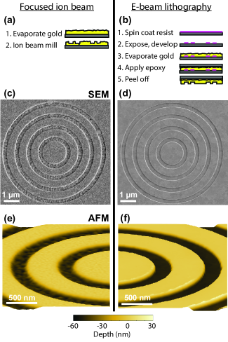
We fabricated bullseye lenses using two processes illustrated in Figure 6. One process involves thermally evaporating 5 nm of titanium as an adhesion layer and 150 nm of gold onto a Si wafer, then carving out the rings using focused-ion-beam (FIB) milling. A Zeiss Crossbeam 1540 EsB is used for the FIB. The other process uses electron-beam lithography followed by template stripping to produce high-precision, smooth cathode surfaces Vogel et al. (2012). A negative e-beam resist hydrogen silsesquioxane (HSQ) is spun at 1000 rpm onto a Si wafer. The resist is then exposed using a Vistec VB300 electron-beam lithography (EBL) system and developed, leaving the designed pattern in the form of amorphous silica on the wafer. Then, 150 nm of gold was deposited onto the template, entirely covering it. Finally, the patterned gold is peeled off using an electrically and thermally conductive ultra-high-vacuum compatible epoxy resin. Atomic force microscopy (AFM) measurements confirm that similar groove depths can be made in both structures, but the EBL and template stripping process yields smoother surfaces and grooves. In fact, structures made by EBL have nearly atomically flat central areas, which minimizes degradation of the emitted electron beam from surface roughness and imperfections Lau (1987) (see Table 1). In these lenses, the gratings are 50 nm deep with parameters otherwise matching the first case (783-nm period, 270-nm width, four rings): its simulated spectral response is shown in Figure 4.
| FIB | EBL | |
|---|---|---|
| Groove depth (nm) | 51 | 54 |
| Center RMS roughness (nm) | 1.4 | 0.4 |
| Groove RMS roughness (nm) | 3.2 | 0.6 |
IV Cathodoluminescence spectromicroscopy
IV.1 Examining plasmonic properties
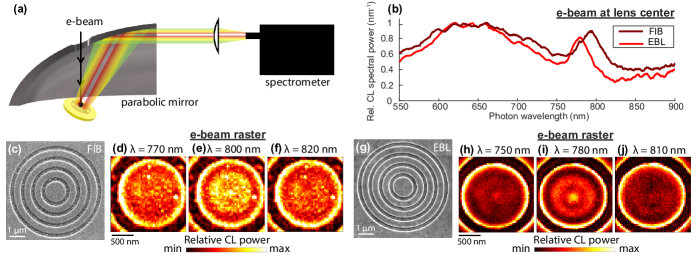
Here, we present cathodoluminescence (CL) spectromicroscopy measurements of plasmonic characteristics of fabricated lenses. In CL, an electron beam is focused on the sample and, by one or more mechanisms, light is emitted from the material De Abajo (2010). For plasmonic structures, the relevant mechanism is the broadband generation of SPPs by the fast-moving electrons as they strike the material surface. The SPPs propagate radially outward from a nanometric spot, which can then couple out to light through the bullseye grating Kuttge et al. (2009); Hofmann et al. (2007). When the electron beam is at the bullseye center, circularly symmetric SPPs are excited like those that would be generated by a radially polarized laser.
We use CL to measure a few key plasmonic properties of these structures. For one, the plasmonic resonance in the central region can be mapped using CL spectromicroscopy. CL intensity has been linked to the radiative local density of optical states (LDOS) at the electron beam position, ie. the number of optical modes available at the excitation position that produce light Kuttge et al. (2009); Losquin and Kociak (2015). The LDOS is enhanced by plasmonic resonance, so CL can be used to spatially and spectrally resolve resonance modes Coenen et al. (2015); Kociak et al. (2014). Spatial homogeneity, circular symmetry, and a strong, sharp central peak are desirable for photoemission applications. The center wavelength and bandwidth of this resonance can be extracted from the CL spectrum obtained at the structure center. Also, the radial extent and circular symmetry of plasmon propagation and grating coupling can be inferred by angle-resolved imaging of the CL far field, which is essentially a Fourier transform of the real-space emission profile of the structure. These are important to characterize since significant propagation losses or asymmetries in coupling would reduce the field enhancement under laser illumination.
We use a modified Zeiss Gemini SUPRA 55 SEM for our CL measurements. The sample is positioned at the focal point of a horizontal Al parabolic mirror with 1 mm focal length. A 10-keV electron beam is focused onto the sample, and the emitted light is collected by the parabolic mirror over a wide angle range ( - from normal) and over the entire visible spectrum and beyond. The sample was tilted by about so that the highly directed, normal emission would not escape through the entry hole in the mirror for the electron beam. We do not expect this tilt to change the plasmonic response; there will not be significant arrival time delay across the electron beam since it is much smaller than the plasmon wavelength. Also, the electron beam only generates SPPs at the surface, so the source size is only made about 10% larger along the tilt direction.
IV.2 CL spectromicroscopy of plasmonic resonance
We use scanning CL spectromicroscopy to probe the spectral and spatial characteristics of the surface-plasmon resonance in our fabricated lenses. The electron beam is rastered step by step over the central plateau of the structure, and a full CL-emission spectrum is collected at each beam position. Spectra are obtained by focusing the reflected light from the mirror onto a multi-mode optical fiber with a 200 m diameter and then dispersing it using a spectrometer consisting of an Acton 2300i monochromator (150 line/mm, 500 nm blazed grating) and Andor Newton electron-multiplied charge-coupled device (CCD). The dark current background is subtracted and spectra are normalized by the instrument response over the measured wavelength range. The open-source Python-based ScopeFoundry software developed to control this experiment is available online for further reference Durham et al. (2018); Barnard .
From this 3D data set, we can extract average emission spectra from regions of interest. Average spectra over the region within 75 nm of the bullseye center are shown in Figure 7a. Spectra shown here are smoothed using a second-order Savitsky-Golay filter with 15-nm window. The CL emission spans the entire detection spectral range. This is because a SPP of any wavelength from the broadband range generated by the electron beam can satisfy the grating equation and couple to light at a wavelength-dependent emission angle, and nearly all emission angles are collected by the parabolic mirror. However, there is a notable emission peak near 800 nm where a surface plasmon resonance is expected.
We can then examine the spatial profile of the plasmonic resonance. We apply virtual Gaussian bandpass filters with 2 = 10 nm to the entire dataset, yielding maps of CL emission over narrow spectral bands as a function of beam position [see Figure 7c-j]. For maps of emission near the resonance wavelength, a zero-order Bessel-function spatial profile is observed corresponding to a cylindrical plasmonic resonance of the central plateau. For the maps at wavelengths just outside of the resonance peak, such a spatial profile is not observed, confirming that it is a resonance effect. For the structure made by EBL, the CL intensity is higher when the structure is excited at the central peak antinode than at the nearby annular antinode. For the structure made by FIB, however, the CL intensity is similar when exciting at either antinode. This suggests that the constructive interference of SPP modes from different directions is improved in the EBL structures, leading to a stronger central peak.
Other features in the maps are also present off resonance. For instance, bright spots are present in the map of the FIB-milled structure [Figure 7d-f] which correspond to bright signals in the secondary electron image [Figure 7c]. The groove edges are brighter in both structures regardless of wavelength. These correspond to topographic features with locally high surface area and roughness, which can enhance the radiative LDOS by scattering more SPP modes out to light. The near-atomic smoothness of the central region in the EBL structures eliminates the scattering sites observed in the FIB structure. This will reduce damping of the resonance and thereby improve the field enhancement under laser illumination and consequently the amount of emitted electrons.
We note that there are key differences between CL mapping and the FDTD simulations used in section II. The excitation mechanism is different: FDTD simulates a radially polarized laser excitation and calculates the field enhancement at all positions, whereas CL mapping rasters an e-beam and collects the integrated light output as a function of e-beam position. This scanning local excitation provides a different spatial profile than expected for a global laser excitation based on FDTD. For instance, the CL emission is stronger when the electron beam is positioned at edges than the structure center, but this is not expected for the case of radially polarized illumination. Still, we can use CL mapping to visualize scattering sites and study the symmetry and smoothness of the plasmonic resonance mode, as discussed above. For more detailed discussion of the CL dependence on electron beam position, see the Appendix.
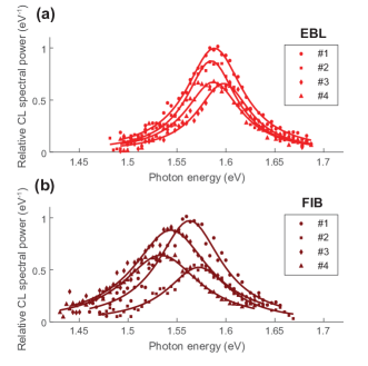
To quantify and compare the resonance characteristics of structures made by FIB and EBL, we fit the resonance peaks in CL spectra collected using an e-beam at the lens center (where the plasmons generated match the circular symmetry of the structure) to determine the resonance wavelength and the FWHM. Average spectra from scan positions within 75 nm of the bullseye center are extracted from spectromicroscopy scans. The spectra are then re-binned into 2-nm wavelength bins and converted from wavelength to energy scale. The resonance peak is fit using a Lorentzian plus a parabolic background. Four structures made by each fabrication method were measured and analyzed. The converted spectra and peak fitting are shown in Figure 8. The average resonance wavelength is 798.4 8.8 nm standard deviation for the FIB-milled structures and 779.6 2.4 nm for the EBL structures. Both are near the 794-nm resonance wavelength predicted by FDTD for structures with the fabricated dimensions. The average measured frequency-to-FWHM ratio, or Q factor, is 17.8 2.0 for the FIB-milled structures and 23.9 1.9 for the EBL structures. The more precise resonance wavelength and higher Q factor (lower damping) of the EBL structures can be attributed to the reproducibility of the structure dimensions and their smoothness.
IV.3 Angle-resolved CL and photon-plasmon coupling
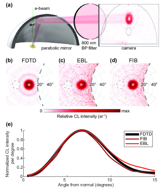
We study the angle-resolved CL emission to infer the radial extent of effective plasmon propagation and grating coupling in the fabricated lenses. We both simulate and measure the CL far field for four- and 12-ring bullseye lenses. The far field is measured by positioning the electron beam at the structure center and imaging the parabolic mirror Coenen et al. (2011, 2014). Because the emitting structure (several micrometers) is small compared to the distance from the mirror (1 mm), the position where an emitted photon reflects from the mirror is determined by the emission angle. The parabolic mirror brings the emission to infinity focus, which is filtered by a bandpass filter centered at 800 nm with 40 nm bandwidth and then magnified and imaged onto a ThorLabs DCC3260M CMOS camera. For each measurement, 30 one-second exposures of the CCD are acquired and averaged. A background image with the beam blanked is acquired under the same conditions and is subtracted from the beam-on image. Then, each pixel in the image is mapped to an emission angle, and the signal is normalized by the solid angle collected by that pixel to give an intensity map. The measured far field is then corrected for tilt and rotation of the sample relative to the mirror.
Using FDTD, the CL process can be numerically modeled Lumerical . An impinging 10-keV electron at the center of the bullseye is modeled using a series of dipoles normal to the surface. The dipoles are delayed in phase to create a propagating, localized source of electric field. This generates a time- and z-dependent current density close to that of a moving electron Chaturvedi et al. (2009): . Here, is the fundamental charge, is the speed of the impinging electron, is the unit vector in the z direction, and and give the lateral position of the impinging electron. The resulting field decays laterally, and vanishes within a few nm in the metal; therefore, no field can directly couple to the grooves, and all observed emission is due to generation, propagation, and outcoupling of SPPs. To avoid abrupt appearance and disappearance of the dipole field, which would create stray fields, a raised-cosine filter is used to gradually increase and decrease the amplitude oscillations of the starting and ending dipoles in time. The simulation box was gradually increased in order to collect larger angles and mesh dimension was decreased to achieve convergence.
Simulated and measured far-field CL of four-ring lenses are shown in Figure 9a-c. A donut beam is observed in all cases, supporting that the emission is radially polarized. Other work performing CL polarimetry on bullseyes has resolved the angle-dependent polarization state and verified that the emission is radially polarized Osorio et al. (2015). Both the angle of maximum emission and the overall angular distribution measured for lenses made by EBL and FIB closely match that predicted using FDTD (see Figure 9d). This indicates that the radial distribution of CL emission from plasmon-photon coupling is robust to fabrication imperfections, including the surface roughness of the FIB-milled structure. These measurements also show that this normally directed emission is captured effectively at 25∘ sample tilt; this supports the validity of the spectra shown above and demonstrates the need for tilting the sample to study this emission.
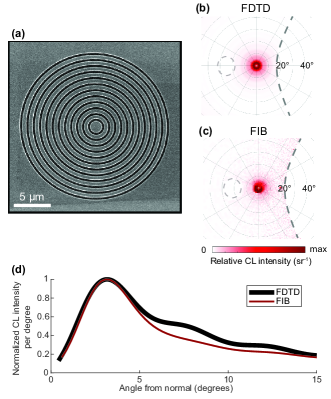
We also fabricated and studied a 12-ring bullseye lens using FIB as shown in Figure 10a. The simulated and measured far-field for this structure are shown in 10b-c. Again, a donut beam is produced as expected. The far field is more asymmetric than for the four-ring structures, which may be due to challenges in making the outer rings accurately concentric with the inner rings using FIB. Still, the angular breadth of emission is greatly reduced, indicating that the plasmons can outcouple over a greater radial extent. As highlighted in Figure 10d, the peak emission angle is 3∘, whereas in the four-ring lenses it was 7∘. The distribution matches well between simulation and experiment overall, especially at less than 5∘. This suggests that additional plasmon propagation losses due to polycrystallinity are not a limiting factor even for this 12-ring structure.
V Conclusions
We have presented a novel design for ultrafast nanoscale electron emitters which has several advantages for the next generation of electron-based instrumentation. First, the design is compatible with high accelerating fields while decreasing the source size by two orders of magnitude as compared to an unpatterned flat cathode. Electromagnetic simulations and cathodoluminescence mapping support that plasmonic resonance leads to a single dominant central peak in optical intensity which could be used to generate electron pulses with 140-nm FWHM (60-nm RMS) lateral size. Second, the emission surface can be made nearly atomically flat, suppressing emittance increase from surface roughness and from aberrations due to field curvature, differently from what happens with tips. Thirdly, the geometric parameters can be tuned to optimize the photocurrent and temporal response for application requirements without changing the emission spot size. The computations and experiments shown here support that the plasmonic properties and the spectral bandwidth of such structures are compatible with emission of sub-10-fs pulses.
These plasmonic lenses could also facilitate emerging high-intensity modes of operation. For instance, they reduce the laser power required to access the optical field emission regime, in which the fields are strong enough to modulate the work function at the optical frequency. This operating regime is of great interest because it allows control of the photocurrent density at attosecond timescales, providing the potential to generate attosecond electron-pulse trains Krüger et al. (2012). In addition, the compatibility of these lenses with few-cycle pulses could allow control of the photocurrent intensity by tuning the carrier envelope phase, as has been demonstrated for tip emitters Piglosiewicz et al. (2014).
In terms of applications, the transverse brightness of such nanocathodes is expected to be more than 1 order of magnitude better than present state of art flat cathodes. Their use in rf environments would enable production of relativistically accelerated electrons with picometer emittance, which could be focused down to nanometer sizes and efficiently injected into advanced acceleration devices England et al. (2014). In ultrafast electron imaging, such sources promise to bridge the gap in spatial resolution between static and ultrafast relativistic sources, applying electron-based characterization to nanoscale dynamics.
Acknowledgements.
D.F. and the work at the Molecular Foundry were supported by the Office of Science, Office of Basic Energy Sciences, of the U.S. Department of Energy under Contract No. DE-AC02-05CH11231. Funding for D.B.D. was provided by STROBE: A National Science Foundation Science and Technology Center under Grant No. DMR 1548924. We thank F. Ogletree, S. Aloni, and E.S. Barnard at the Molecular Foundry for their advice and assistance with the CL setup. We thank S. Dhuey at the Molecular Foundry for assistance with the e-beam lithography. D.B.D. and F.R. contributed equally to this work.*
Appendix A CL dependence on electron beam position
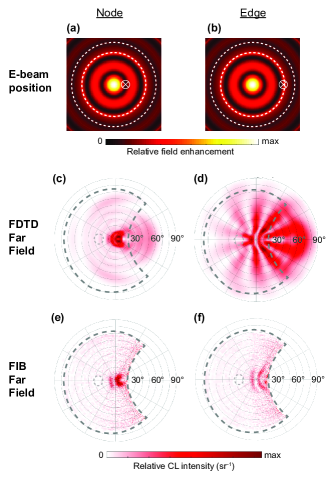
As discussed in section IV, scanning CL can be used to obtain qualitative maps of the plasmonic resonance and, more generally, the radiative LDOS. These are fundamentally different from the field enhancement profile expected upon excitation with a radially polarized beam. The main difference is that the electron beam only excites purely radial plasmon modes in the structure when the beam is positioned at the center. Elsewhere, the beam generates SPPs traveling outward from its current position rather than the lens center, so the modes excited do not match the circular symmetry of the lens. This plasmonic configuration would not be excited by a radially polarized laser.
Using angle-resolved CL, we can observe this symmetry mismatch between plasmons and lens for off-center electron beam positions, shown in Figure 11 for a 4-ring lens. Instead of a circularly symmetric donut-shaped emission, complex interference patterns are generated in the far field whose shape depends on the beam position Osorio et al. (2015).
For this reason, it is hard to quantitatively compare spatial profiles from CL spectromicroscopy and simulated field enhancement under laser illumination. One example of this is the observation that the CL emission is brighter when the beam is at the groove edge than at the center of the structure (see Figure 7). At the edge, the plasmon modes excited and how they couple to the structure are much different than when the beam is at the center, as evidenced by the far field shown in Figure 11d,f. Also, the edge is a strong scattering site, allowing many SPP modes generated nearby to couple to light, giving an enhanced radiative LDOS. Therefore, we still expect that the field enhancement and consequent photoemission under laser illumination will be stronger at the center than the edges.
Quantitative analysis of the spatial map is further complicated by the nature of the CL process. The total measured intensity of this emission depends on how the emission interferes in the far field and what parts of the emission are collected by the mirror. At both the node and edge positions, some of the emitted light is not collected by the mirror (see Figure 11c-f). Still, valuable qualitative insight can be obtained from scanning CL as discussed in Section IVB, such as visualizing the plasmonic resonance mode and nanoscale heterogeneities.
References
- Siwick et al. (2003) Bradley J Siwick, Jason R Dwyer, Robert E Jordan, and RJ Dwayne Miller, “An atomic-level view of melting using femtosecond electron diffraction,” Science 302, 1382–1385 (2003).
- Morrison et al. (2014) Vance R Morrison, Robert P Chatelain, Kunal L Tiwari, Ali Hendaoui, Andrew Bruhács, Mohamed Chaker, and Bradley J Siwick, “A photoinduced metal-like phase of monoclinic VO2 revealed by ultrafast electron diffraction,” Science 346, 445–448 (2014).
- Eichberger et al. (2010) Maximilian Eichberger, Hanjo Schäfer, Marina Krumova, Markus Beyer, Jure Demsar, Helmuth Berger, Gustavo Moriena, Germán Sciaini, and RJ Dwayne Miller, “Snapshots of cooperative atomic motions in the optical suppression of charge density waves,” Nature 468, 799 (2010).
- Zewail (2006) Ahmed H Zewail, “4D ultrafast electron diffraction, crystallography, and microscopy,” Annu. Rev. Phys. Chem. 57, 65–103 (2006).
- Gao et al. (2013) Meng Gao, Cheng Lu, Hubert Jean-Ruel, Lai Chung Liu, Alexander Marx, Ken Onda, Shin-ya Koshihara, Yoshiaki Nakano, Xiangfeng Shao, Takaaki Hiramatsu, et al., “Mapping molecular motions leading to charge delocalization with ultrabright electrons,” Nature 496, 343 (2013).
- Rhee (1992) M. J. Rhee, “Refined definition of the beam brightness,” Physics of Fluids B: Plasma Physics 4, 1674–1676 (1992).
- Carbone et al. (2012) F. Carbone, P. Musumeci, O.J. Luiten, and C. Hebert, “A perspective on novel sources of ultrashort electron and X-ray pulses,” Chemical Physics 392, 1–9 (2012).
- Feist et al. (2018) Armin Feist, Nara Rubiano da Silva, Wenxi Liang, Claus Ropers, and Sascha Schäfer, “Nanoscale diffractive probing of strain dynamics in ultrafast transmission electron microscopy,” Structural Dynamics 5, 014302 (2018).
- da Silva et al. (2018) Nara Rubiano da Silva, Marcel Möller, Armin Feist, Henning Ulrichs, Claus Ropers, and Sascha Schäfer, “Nanoscale mapping of ultrafast magnetization dynamics with femtosecond lorentz microscopy,” Physical Review X 8, 031052 (2018).
- Yurtsever et al. (2012) Aycan Yurtsever, Renske M van der Veen, and Ahmed H Zewail, “Subparticle ultrafast spectrum imaging in 4D electron microscopy,” Science 335, 59–64 (2012).
- Maxson et al. (2017) Jared Maxson, David Cesar, Giacomo Calmasini, Alexander Ody, Pietro Musumeci, and David Alesini, “Direct measurement of sub-10 fs relativistic electron beams with ultralow emittance,” Physical Review Letters 118 (2017), 10.1103/PhysRevLett.118.154802.
- Zhao et al. (2018) Lingrong Zhao, Zhe Wang, Chao Lu, Rui Wang, Cheng Hu, Peng Wang, Jia Qi, Tao Jiang, Shengguang Liu, Zhuoran Ma, Fengfeng Qi, Pengfei Zhu, Ya Cheng, Zhiwen Shi, Yanchao Shi, Wei Song, Xiaoxin Zhu, Jiaru Shi, Yingxin Wang, Lixin Yan, Liguo Zhu, Dao Xiang, and Jie Zhang, “Terahertz streaking of few-femtosecond relativistic electron beams,” Physical Review X 8 (2018), 10.1103/PhysRevX.8.021061.
- Huang et al. (2015) R. Huang, D. Filippetto, C.F. Papadopoulos, H. Qian, F. Sannibale, and M. Zolotorev, “Dark current studies on a normal-conducting high-brightness very-high-frequency electron gun operating in continuous wave mode,” Physical Review Special Topics - Accelerators and Beams 18 (2015), 10.1103/PhysRevSTAB.18.013401.
- Polyakov et al. (2013) Aleksandr Polyakov, Christoph Senft, KF Thompson, J Feng, S Cabrini, PJ Schuck, HA Padmore, Samuel J Peppernick, and Wayne P Hess, “Plasmon-enhanced photocathode for high brightness and high repetition rate x-ray sources,” Physical review letters 110, 076802 (2013).
- Li et al. (2013) RK Li, H To, G Andonian, J Feng, A Polyakov, CM Scoby, K Thompson, W Wan, HA Padmore, and P Musumeci, “Surface-plasmon resonance-enhanced multiphoton emission of high-brightness electron beams from a nanostructured copper cathode,” Physical review letters 110, 074801 (2013).
- Lau (1987) Y. Y. Lau, “Effects of cathode surface roughness on the quality of electron beams,” Journal of Applied Physics 61, 36–44 (1987), https://doi.org/10.1063/1.338833 .
- Steele et al. (2006) Jennifer M Steele, Zhaowei Liu, Yuan Wang, and Xiang Zhang, “Resonant and non-resonant generation and focusing of surface plasmons with circular gratings,” Optics Express 14, 5664–5670 (2006).
- Chen et al. (2009) Weibin Chen, Don C Abeysinghe, Robert L Nelson, and Qiwen Zhan, “Plasmonic lens made of multiple concentric metallic rings under radially polarized illumination,” Nano letters 9, 4320–4325 (2009).
- Bechtel et al. (1977) JH Bechtel, W Lee Smith, and N Bloembergen, “Two-photon photoemission from metals induced by picosecond laser pulses,” Physical Review B 15, 4557 (1977).
- Kolomenski et al. (2009) Andrei Kolomenski, Alexandre Kolomenskii, John Noel, Siying Peng, and Hans Schuessler, “Propagation length of surface plasmons in a metal film with roughness,” Applied optics 48, 5683–5691 (2009).
- Kuttge et al. (2008) M Kuttge, EJR Vesseur, J Verhoeven, HJ Lezec, HA Atwater, and A Polman, “Loss mechanisms of surface plasmon polaritons on gold probed by cathodoluminescence imaging spectroscopy.” Applied Physics Letters 93, 113110 (2008).
- McPeak et al. (2015) Kevin M McPeak, Sriharsha V Jayanti, Stephan JP Kress, Stefan Meyer, Stelio Iotti, Aurelio Rossinelli, and David J Norris, “Plasmonic films can easily be better: rules and recipes,” ACS photonics 2, 326–333 (2015).
- Olmon et al. (2012) Robert L Olmon, Brian Slovick, Timothy W Johnson, David Shelton, Sang-Hyun Oh, Glenn D Boreman, and Markus B Raschke, “Optical dielectric function of gold,” Physical Review B 86, 235147 (2012).
- Raether (1988) Heinz Raether, “Surface plasmons on gratings,” in Surface plasmons on smooth and rough surfaces and on gratings (Springer, 1988) pp. 91–116.
- (25) Lumerical, “FDTD solutions,” http://www.lumerical.com.
- Laughton and Warne (2003) M A Laughton and D F Warne, Electrical engineer’s reference book, 16th ed. (Elsevier, 2003) pp. 384–387.
- Thio et al. (2001) Tineke Thio, KM Pellerin, RA Linke, HJ Lezec, and TW Ebbesen, “Enhanced light transmission through a single subwavelength aperture,” Optics letters 26, 1972–1974 (2001).
- Hooper and Sambles (2002) Ian R Hooper and J Roy Sambles, “Dispersion of surface plasmon polaritons on short-pitch metal gratings,” Physical Review B 65, 165432 (2002).
- Vogel et al. (2012) Nicolas Vogel, Julius Zieleniecki, and Ingo Köper, “As flat as it gets: ultrasmooth surfaces from template-stripping procedures,” Nanoscale 4, 3820–3832 (2012).
- De Abajo (2010) FJ García De Abajo, “Optical excitations in electron microscopy,” Reviews of modern physics 82, 209 (2010).
- Kuttge et al. (2009) Martin Kuttge, Ernst Jan R Vesseur, AF Koenderink, HJ Lezec, HA Atwater, FJ García de Abajo, and Albert Polman, “Local density of states, spectrum, and far-field interference of surface plasmon polaritons probed by cathodoluminescence,” Physical Review B 79, 113405 (2009).
- Hofmann et al. (2007) Carrie E Hofmann, Ernst Jan R Vesseur, Luke A Sweatlock, Henri J Lezec, F Javier García de Abajo, Albert Polman, and Harry A Atwater, “Plasmonic modes of annular nanoresonators imaged by spectrally resolved cathodoluminescence,” Nano letters 7, 3612–3617 (2007).
- Losquin and Kociak (2015) Arthur Losquin and Mathieu Kociak, “Link between cathodoluminescence and electron energy loss spectroscopy and the radiative and full electromagnetic local density of states,” ACS Photonics 2, 1619–1627 (2015).
- Coenen et al. (2015) Toon Coenen, Benjamin JM Brenny, Ernst Jan Vesseur, and Albert Polman, “Cathodoluminescence microscopy: optical imaging and spectroscopy with deep-subwavelength resolution,” MRS Bulletin 40, 359–365 (2015).
- Kociak et al. (2014) Mathieu Kociak, Odile Stéphan, Alexandre Gloter, Luiz F Zagonel, Luiz HG Tizei, Marcel Tencé, Katia March, Jean Denis Blazit, Zackaria Mahfoud, Arthur Losquin, et al., “Seeing and measuring in colours: Electron microscopy and spectroscopies applied to nano-optics,” Comptes Rendus Physique 15, 158–175 (2014).
- Durham et al. (2018) Daniel B Durham, D Frank Ogletree, and Edward S Barnard, “Scanning Auger spectromicroscopy using the ScopeFoundry software platform,” Surface and Interface Analysis 50, 1174–1179 (2018).
- (37) Edward S Barnard, “ScopeFoundry: A python platform for controlling custom laboratory experiments and visualizing scientific data,” http://www.scopefoundry.org/.
- Coenen et al. (2011) Toon Coenen, Ernst Jan R Vesseur, and Albert Polman, “Angle-resolved cathodoluminescence spectroscopy,” Applied Physics Letters 99, 143103 (2011).
- Coenen et al. (2014) Toon Coenen et al., Angle-resolved cathodoluminescence nanoscopy (Universiteit van Amsterdam [Host], 2014).
- Chaturvedi et al. (2009) Pratik Chaturvedi, Keng H Hsu, Anil Kumar, Kin Hung Fung, James C Mabon, and Nicholas X Fang, “Imaging of plasmonic modes of silver nanoparticles using high-resolution cathodoluminescence spectroscopy,” ACS Nano 3, 2965–2974 (2009).
- Osorio et al. (2015) Clara I Osorio, Toon Coenen, Benjamin JM Brenny, Albert Polman, and A Femius Koenderink, “Angle-resolved cathodoluminescence imaging polarimetry,” ACS Photonics 3, 147–154 (2015).
- Krüger et al. (2012) Michael Krüger, Markus Schenk, Michael Förster, and Peter Hommelhoff, “Attosecond physics in photoemission from a metal nanotip,” Journal of Physics B: Atomic, Molecular and Optical Physics 45, 074006 (2012).
- Piglosiewicz et al. (2014) Björn Piglosiewicz, Slawa Schmidt, Doo Jae Park, Jan Vogelsang, Petra Groß, Cristian Manzoni, Paolo Farinello, Giulio Cerullo, and Christoph Lienau, “Carrier-envelope phase effects on the strong-field photoemission of electrons from metallic nanostructures,” Nature Photonics 8, 37 (2014).
- England et al. (2014) R. Joel England, Robert J. Noble, Karl Bane, David H. Dowell, Cho-Kuen Ng, James E. Spencer, Sami Tantawi, Ziran Wu, Robert L. Byer, Edgar Peralta, Ken Soong, Chia-Ming Chang, Behnam Montazeri, Stephen J. Wolf, Benjamin Cowan, Jay Dawson, Wei Gai, Peter Hommelhoff, Yen-Chieh Huang, Chunguang Jing, Christopher McGuinness, Robert B. Palmer, Brian Naranjo, James Rosenzweig, Gil Travish, Amit Mizrahi, Levi Schachter, Christopher Sears, Gregory R. Werner, and Rodney B. Yoder, “Dielectric laser accelerators,” Reviews of Modern Physics 86, 1337–1389 (2014).