Helical quantum Hall phase in graphene on SrTiO3
Abstract
The ground state of charge neutral graphene under perpendicular magnetic field was predicted to be a quantum Hall topological insulator with a ferromagnetic order and spin-filtered, helical edge channels. In most experiments, however, an otherwise insulating state is observed and is accounted for by lattice-scale interactions that promote a broken-symmetry state with gapped bulk and edge excitations. We tuned the ground state of the graphene zeroth Landau level to the topological phase via a suitable screening of the Coulomb interaction with a SrTiO3 high- dielectric substrate. We observed robust helical edge transport emerging at a magnetic field as low as 1 tesla and withstanding temperatures up to 110 kelvins over micron-long distances. This new and versatile graphene platform opens new avenues for spintronics and topological quantum computation.
There is a variety of topological phases that are classified by their dimensionality, symmetries and topological invariants Hasan and Kane (2010); Qi and Zhang (2011). They all share the remarkable property that the topological bulk gap closes at every interfaces with vacuum or a trivial insulator, forming conductive edge states with peculiar transport and spin properties. The quantum Hall effect that arises in two-dimensional (2D) electron systems subjected to a perpendicular magnetic field, , stands out as a paradigmatic example characterized by the Chern number that quantizes the Hall conductivity and counts the number of chiral, one-dimensional edge channels. The singular aspect of quantum Hall systems compared to time-reversal symmetric topological insulators (TIs) lies in the pivotal role of Coulomb interaction between electrons that can induce a wealth of strongly correlated, symmetry or topologically-protected phases, ubiquitously observed in various experimental systems Tsui et al. (1982); Willett et al. (1987); Du et al. (2009); Bolotin et al. (2009); Maher et al. (2013); Young et al. (2014); Ki et al. (2014); Falson et al. (2015); Zibrov et al. (2018); Kim et al. (2019).
In graphene the immediate consequence of the Coulomb interaction is an instability towards quantum Hall ferromagnetism. Due to exchange interaction, a spontaneous breaking of the SU(4) symmetry splinters the Landau levels into quartets of broken-symmetry states that are polarized in one, or a combination of the spin and valley (pseudospin) degrees of freedom Yang et al. (2006); Nomura and MacDonald (2006); Young et al. (2012).
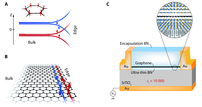
Central to this phenomenon is the fate of the zeroth Landau level and its quantum Hall ground states. It was early predicted that if the Zeeman spin-splitting (enhanced by exchange interaction) overcomes the valley splitting, a topological inversion between the lowest electron-type and highest hole-type sub-levels should occur Abanin et al. (2006); Fertig and Brey (2006). At charge neutrality, the ensuing ground state is a quantum Hall ferromagnet with two filled states of identical spin polarization, and an edge dispersion that exhibits two counter-propagating, spin-filtered helical edge channels (Fig. 1A and B), similar to those of the quantum spin Hall (QSH) effect in 2D TIs König et al. (2007); Knez et al. (2011); Fei et al. (2017); Wu et al. (2018); Hatsuda et al. (2018). Such a spin-polarized ferromagnetic (F) phase belongs to the recently identified new class of interaction-induced TIs with zero Chern number, termed quantum Hall topological insulators Kharitonov et al. (2016) (QHTIs), which arise from a many-body interacting Landau level and can be pictured as two independent copies of quantum Hall systems with opposite chiralities. Remarkably, unlike 2D TIs, immunity from back-scattering for the helical edge channels does not rely on the discrete time-reversal symmetry, conspicuously broken here by the magnetic field, but on the continuous U(1) axial rotation symmetry of the spin polarization Young et al. (2014); Kharitonov et al. (2016).
The experimental situation is however at odds with this exciting scenario. A strong insulating state is systematically observed on increasing perpendicular magnetic field in charge-neutral, high-mobility graphene devices. The formation of the F phase is presumably hindered by some lattice-scale electron-electron and electron-phonon interaction terms, whose amplitudes and signs can be strongly renormalized by the long-range part of the Coulomb interaction Kharitonov (2012a), favoring various insulating spin- or charge-density-wave orders Alicea and Fisher (2006); Jung and MacDonald (2009); Kharitonov (2012a). Only with a very strong in-plane magnetic field component such that Zeeman energy overcomes the other anisotropic interaction terms does the F phase emerge experimentally Young et al. (2014); Maher et al. (2013). Another strategy to engineer a F phase uses small-angle twisted graphene bilayers, with each layer sets in a different quantum Hall state of opposite charge polarity via a displacement field Sanchez-Yamagishi et al. (2017). Yet, those approaches realized hitherto suffer from either unpractical strong and tilted magnetic field or the complexity of the twisted layers assembly.
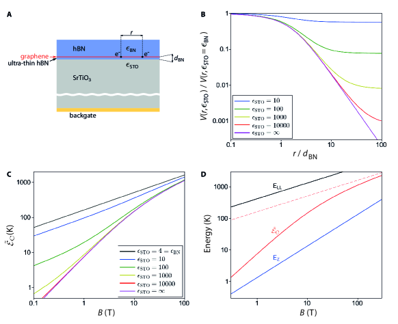
In this work we take a novel route to induce the F phase in monolayer graphene in a straightforward fashion. Instead of boosting the Zeeman effect with a strong in-plane field, we mitigate the effects of the lattice-scale interaction terms by a suitable substrate screening of the Coulomb interaction to restore the dominant role of the spin-polarizing terms and induce the F phase. We use a high- dielectric substrate, the quantum paraelectric SrTiO3 known to exhibit a very large static dielectric constant of the order of at low temperatures Sakudo and Unoki (1971) (see Fig. S3), which acts both as an electrostatic screening environment and back-gate dielectric Couto et al. (2011). For an efficient screening of the Coulomb potential, the graphene layer must be sufficiently close to the substrate, with a separation less than the magnetic length ( the reduced Planck constant, the electron charge), which is the relevant length scale in the quantum Hall regime. High mobility hexagonal boron-nitride (hBN) encapsulated graphene heterostructures Wang et al. (2013) were thus purposely made with an ultra-thin bottom hBN layer with a thickness, , ranging between nm (see Fig. 1C, and see Supplementary Materials ) inferior to the magnetic length for moderate magnetic field (e.g. nm for T).
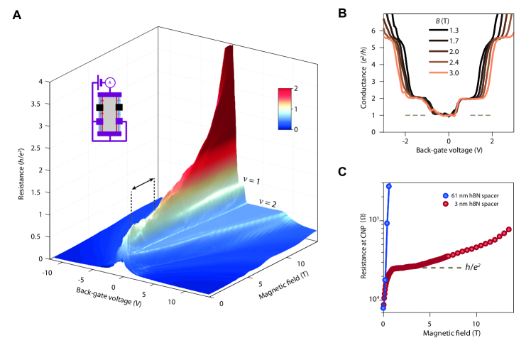
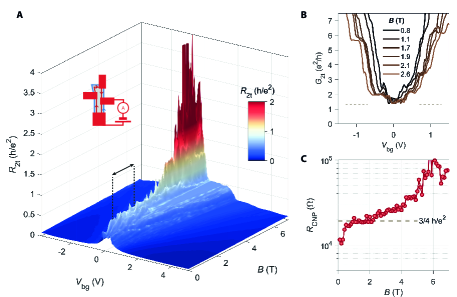
The emergence of the F phase in such a screened configuration is readily seen in Fig. 2A, which displays the two-terminal resistance of a hBN encapsulated graphene device in a six-terminal Hall bar geometry, as a function of the back-gate voltage and magnetic field. Around the charge neutrality ( V), an anomalous resistance plateau develops over a -range from to T indicated by the two dotted black lines. This plateau reaches the quantum of resistance , color-coded in white. At T, the resistance departs from towards insulation as seen by the red color-coded magneto-resistance peak (see also Fig. 2C).
The unusual nature of this resistance plateau can be captured with the line-cuts of the two-terminal conductance versus at fixed , see Fig. 2B. While standard graphene quantum Hall plateaus at and for the Landau level indices and are well developed as a function of back-gate voltage, the new plateau at is centered at the charge neutrality and does not show any dip at V. This behavior is at odds with the usual sequence of broken-symmetry states setting with magnetic field where first the insulating broken-symmetry state opens at with , followed at higher field by the plateaus of the broken-symmetry states at filling fraction Nomura and MacDonald (2006); Young et al. (2012). In Figure 2A, the latter states at arise for T together with the insulating magnetoresistance peak at , that is, above the field range of the anomalous plateau. Hence, this striking observation of a plateau at low magnetic field conspicuously points to a new broken-symmetry state at . We show in the following that this plateau is a direct signature of the QSH effect resulting from the helical edge channels of the F phase.
Helical edge transport has unambiguous signatures in multi-terminal device configuration as each ohmic contact acts as a source of back-scattering for the counter-propagating helical edge channels with opposite spin-polarization Roth et al. (2009). An edge section between two contacts is indeed an ideal helical quantum conductor of quantized resistance . The two-terminal resistance of a device therefore ensues from the parallel resistance of both edges, each of them being the sum of contributions of each helical edge sections. As a result,
| (1) |
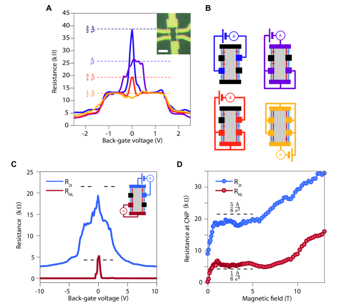
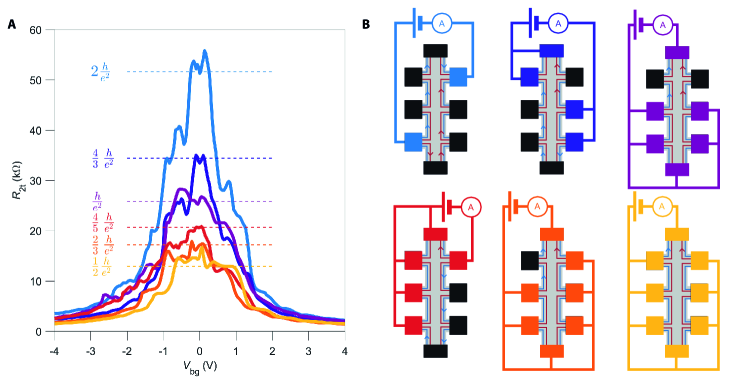
where N is the number of helical conductor sections for the left (L) and right (R) edge between the source and drain contacts Young et al. (2014). By swapping the source and drain contacts for various configurations of N, one expects to observe resistance plateaus given by Eq. (1). Figure 3A displays a set of four different configurations of two-terminal resistances measured at T as a function of back-gate voltage. Swapping the source and drain contacts and the number of helical edge sections (see contact configurations in Fig. 3B) yields a maximum around charge neutrality which reaches the expected values indicated by the dotted horizontal lines, thereby demonstrating helical edge transport. Notice that the plateau at in Fig. 2A is also fully consistent with Eq. (1) for .
Four-terminal non-local configuration provides another stark indicator for helical edge transport Roth et al. (2009). Figure 3C shows simultaneous measurements of the two-terminal resistance between the two blue contacts (see sample schematics in the inset), and the non-local resistance measured on the red contacts while keeping the same source and drain current-injection contacts. While nearly reaches the expected value indicated by the dashed lines, namely ( and ), a non-local voltage develops in the range that coincides with the helical edge transport regime in . The large value of this non-local signal, much larger than what could be expected in the diffusive regime, demonstrates that current is flowing on the edges of the sample. For helical edge transport, the expected non-local resistance is given by , where N and N are the number of helical conductor sections between the source and drain contacts along the edge of the non-local voltage probes and between the non-local voltage probes, respectively. The measured shown in Fig. 3C is in excellent agreement with the expected value (N and N) indicated by the dashed line.
This global set of data that are reproduced on several samples see Supplementary Materials therefore provides compelling evidence for helical edge transport, substantiating the F phase as the ground state at charge neutrality of substrate-screened graphene.
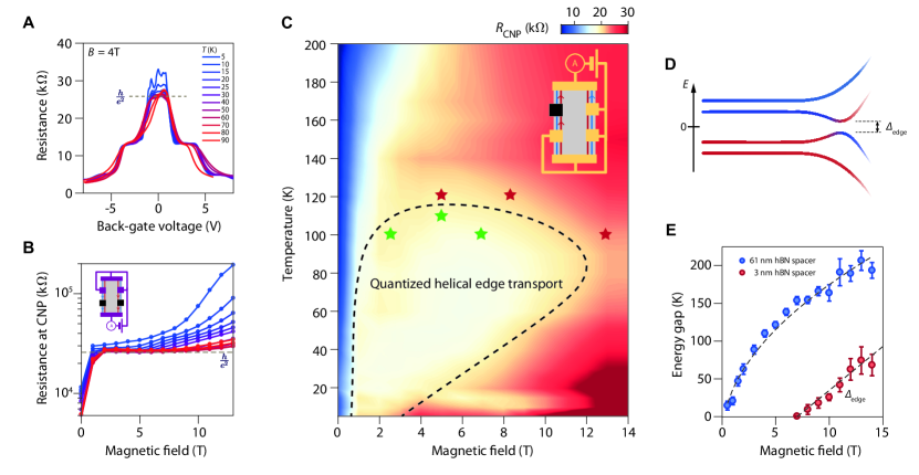
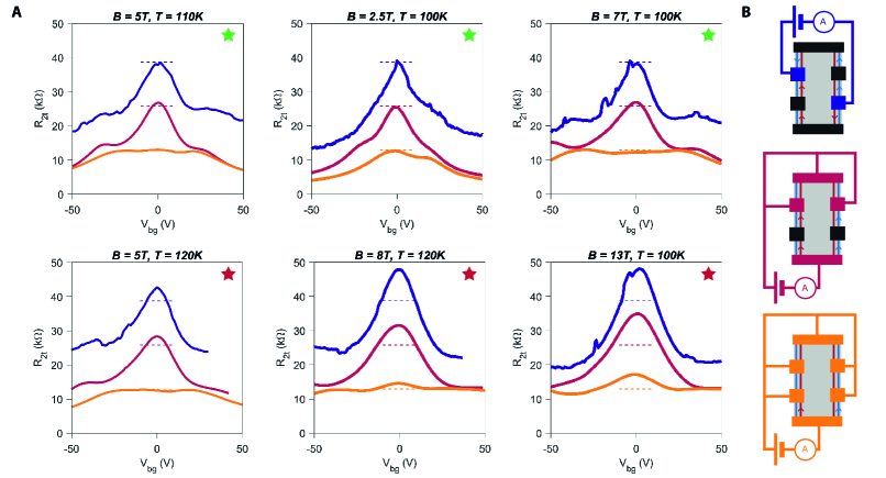
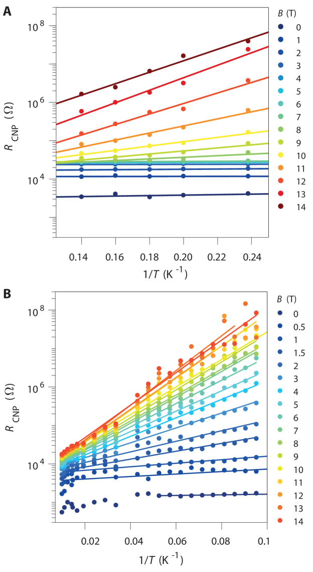
To assess the robustness of the helical edge transport we conducted systematic investigations of its temperature, , and magnetic-field dependences. Figure 4C displays a color-map of the two-terminal resistance of sample BNGrSTO-07 measured at charge neutrality as a function of magnetic field and temperature. The expected resistance value for the contact configuration shown in the inset schematics is . This quantized resistance value is matched over a remarkably wide range of temperature and magnetic field, which is delimited by the dashed black line, confirming the metallic character of the helical edge transport. To ascertain the limit of quantized helical edge transport we measured different contact configurations at some bordering magnetic field and temperature values (see Fig. S7), indicated in Fig. 4C by the green and red stars for quantized and not quantized resistance, respectively. The temperature and magnetic field dependences are further illustrated by Fig. 4A and B, which show the two-terminal resistance (measured in a different contact configuration, see inset Fig. 4B) versus back-gate voltage and the resistance at the charge neutrality point versus , respectively, for various temperatures.
These data show that quantized helical edge transport withstands very high temperatures, up to K, with an onset at T virtually constant in temperature. Such a broad temperature range is comparable to WTe2 for which QSH effect was observed in 100 nm-short channels up to K Wu et al. (2018). The new aspect of the F phase of graphene is that the helical edge channels formed by the broken-symmetry states retain their topological protection over large distances at elevated temperatures, namely m for the helical edge section between contacts of the sample measured in Fig. 4A-C. Various mechanisms can account for the high temperature breakdown of the helical edge transport quantization, such as activation of bulk charge carriers or inelastic scattering processes that break the U(1) spin-symmetry of the QHTI Kharitonov et al. (2016). As the former would reduce resistance by opening conducting bulk channels, the upward resistance deviation upon increasing rather points to inelastic processes that do not conserve spin-polarization. Consequently, this suggests that quantized helical edge transport may be retained at even higher temperatures for lengths below m.
Interestingly, the high magnetic field limit in Fig. 4C is temperature dependent. The lower the temperature the earlier in magnetic field start deviations from quantization: At K, we observe an increase of resistance on increasing from about T (see Fig. 2A and C and Fig. 4A-C), whereas this limit moves to T at K. For T, the resistance exhibits an activated insulating increase with lowering temperature, with a corresponding activation energy that increases linearly with (see Fig. 4E, red points. Data are taken on a different sample exhibiting an onset to insulation at T). Such a behaviour indicates a gap opening in the edge excitation spectrum as illustrated in the Fig. 4D schematics, breaking down the helical edge transport at low temperature. This linear -dependence of the activation energy further correlates with the high magnetic field limit of the helical edge transport in Fig. 4C, thereby explaining why the limit for quantized helical edge transport increases to higher magnetic field with .
The origin of the gap in the edge excitation spectrum is most likely rooted in the enhancement of correlations with magnetic field. An interaction-induced topological quantum phase transition from the QHTI to one of the possible insulating, topologically trivial quantum Hall ground states with spin or charge density wave order is a possible scenario Kharitonov et al. (2016). Such a transition is expected to occur without closing the bulk gap Young et al. (2014); Kharitonov et al. (2016), which we confirmed via bulk transport measurements performed in a Corbino geometry (see Fig. S8). Yet the continuous transition involves complex spin and isospin textures at the edges due to the -enhanced isospin anisotropy Kharitonov (2012b), yielding the edge gap detected in Hall bar geometry. Another scenario relies on the helical Luttinger liquid Wu et al. (2006) behaviour of the edge channels, for which a delicate interplay between -enhanced correlations, disorder and coupling to bulk charge-neutral excitations may also yield activated insulating transport Tikhonov et al. (2016).
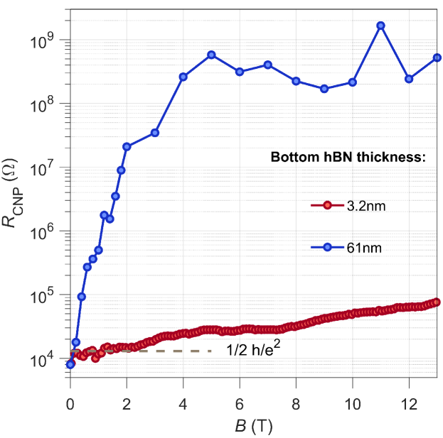
To firmly demonstrate the key role of the SrTiO3 dielectric substrate in the establishment of the F phase, we conducted identical measurements on a sample made with a nm thick hBN spacer, much thicker than at the relevant magnetic fields of this study, so that screening by the substrate is irrelevant in the quantum Hall regime. Shown in Fig. 2C with the blue dots, the resistance at the charge neutrality point diverges strongly upon applying a small magnetic field, thus clearly indicating an insulating ground state without edge transport. Systematic study of the activated insulating behaviour leads to an activation gap that grows as (see blue dots in Fig. 4E and Fig. S9), as expected for a charge excitation gap that scales as the Coulomb energy where and are the vacuum permittivity and the relative permittivity of hBN. This self-consistently demonstrates that the F phase emerges as a ground state due to a significant reduction of the electron-electron interactions by the high- dielectric environment.
Understanding the substrate-induced screening effect for our sample geometry requires electrostatic considerations that take into account the ultra-thin hBN spacer between the graphene and the substrate see Supplementary Materials . The resulting substrate-screened Coulomb energy scale is suppressed by a screening factor where is the relative permittivity of SrTiO3. As a result, electrons in the graphene plane are subject to an unusual -dependent screening that depends on the ratio and is most efficient at low magnetic field (Fig. S11). Importantly, despite the huge dielectric constant of SrTiO3 of the order of (Fig. S3), is scaled down by a factor 10 for due to the hBN spacer, which is still a significant reduction of the long-range Coulomb interaction.
How such a screening affects the short-range, lattice-scale contributions of the Coulomb and electron-phonon interactions that eventually determine the energetically favorable ground state is a challenging question since the hBN spacer precludes screening at the lattice scale. While theoretical estimates of these anisotropy terms initially point to the spin-polarized F ground state, renormalization effects due to the long-range part of the Coulomb interaction Aleiner et al. (2007); Basko and Aleiner (2008) result in anisotropy terms that can change signs and amplitudes in an unpredictable fashion Kharitonov (2012a). The insulating behaviour commonly observed in usual samples still points to a canted anti-ferromagnetic order at charge neutrality, bearing out the strong renormalization of the anisotropy terms. We conjecture that the reduction of the Coulomb energy scale by the substrate screening is the key that suppresses the renormalization effects, restoring the F phase as the ground state at charge neutrality. Therefore, enhancing the Coulomb energy scale by decreasing the ratio induces a topological quantum phase transition from the QHTI ferromagnetic phase to an insulating, trivial quantum Hall ground state.
Finally, our work demonstrates that the F phase in screened graphene, which emerges at low magnetic field, provides a prototypical, interaction-induced topological phase, exhibiting remarkably robust helical edge transport in a wide parameter range. The role of correlations in the edge excitations, which are tunable via the magnetic field and an unusual -dependent screening, should be of fundamental interest for studies of zero-energy modes in superconductivity-proximitized architectures constructed on the basis of helical edge states Fu and Kane (2009); Zhang and Kane (2014); San-Jose et al. (2015). We further expect that substrate-screening engineering, tunable via the hBN spacer thickness, could have implications for many other correlated 2D systems for which the dielectric environment drastically impact their ground states and (opto)electronic properties.
Acknowledgments
We thank H. Courtois, M. Goerbig, M. Kharitonov, A. MacDonald, and A. Grushin for valuable discussions. Samples were prepared at the Nanofab facility of Néel Institute. This work was supported by the H2020 ERC grant QUEST No. 637815. K.W. and T.T. acknowledge support from the Elemental Strategy Initiative conducted by the MEXT, Japan, A3 Foresight by JSPS and the CREST (JPMJCR15F3), JST. Z.H. acknowledges the support from the National Key R&D Program of China (2017YFA0206302), the National Natural Science Foundation of China (NSFC) with Grant 11504385, and the Program of State Key Laboratory of Quantum Optics and Quantum Optics Devices (No. KF201816).
References
- Hasan and Kane (2010) M. Z. Hasan and C. L. Kane, “Colloquium: Topological insulators,” Rev. Mod. Phys. 82, 3045–3067 (2010).
- Qi and Zhang (2011) Xiao-Liang Qi and Shou-Cheng Zhang, “Topological insulators and superconductors,” Rev. Mod. Phys. 83, 1057–1110 (2011).
- Tsui et al. (1982) D. C. Tsui, H. L. Stormer, and A. C. Gossard, “Two-Dimensional Magnetotransport in the Extreme Quantum Limit,” Phys. Rev. Lett. 48, 1559–1562 (1982).
- Willett et al. (1987) R. Willett, J. P. Eisenstein, H. L. Störmer, D. C. Tsui, A. C. Gossard, and J. H. English, “Observation of an even-denominator quantum number in the fractional quantum Hall effect,” Phys. Rev. Lett. 59, 1776–1779 (1987).
- Du et al. (2009) X. Du, I. Skachko, F. Duerr, A Luican, and A. Y. Andrei, “Fractional quantum Hall effect and insulating phase of Dirac electrons in graphene,” Nature 462, 192–195 (2009).
- Bolotin et al. (2009) K. I. Bolotin, F. Ghahari, M. D. Shulman, H. L. Stormer, and P. Kim, “Observation of the fractional quantum Hall effect in graphene,” Nature 462, 196–199 (2009).
- Maher et al. (2013) P. Maher, C. R. Dean, A. F. Young, T. Taniguchi, K. Watanabe, K. L. Shepard, J. Hone, and P. Kim, “Evidence for a spin phase transition at charge neutrality in bilayer graphene,” Nature Physics 9, 154 (2013).
- Young et al. (2014) A. F Young, J. D. Sanchez-Yamagishi, B. Hunt, S. H. Choi, K. Watanabe, T. Taniguchi, R. C. Ashoori, and P. Jarillo-Herrero, “Tunable symmetry breaking and helical edge transport in a graphene quantum spin Hall state,” Nature 505, 528–532 (2014).
- Ki et al. (2014) D.-K. Ki, V.I. Falko, D.A. Abanin, and A.F. Morpurgo, “Observation of even denominator fractional quantum Hall effect in suspended bilayer graphene,” Nano letters 14, 2135–2139 (2014).
- Falson et al. (2015) J. Falson, D. Maryenko, B. Friess, D. Zhang, Y. Kozuka, A. Tsukazaki, J.H. Smet, and M. Kawasaki, “Even-denominator fractional quantum Hall physics in ZnO,” Nature Physics 11, 347–351 (2015).
- Zibrov et al. (2018) A.A. Zibrov, E.M. Spanton, H. Zhou, C. Kometter, T. Taniguchi, K. Watanabe, and A.F. Young, “Even-denominator fractional quantum Hall states at an isospin transition in monolayer graphene,” Nature Physics 14, 930–935 (2018).
- Kim et al. (2019) Y. Kim, A.C. Balram, T. Taniguchi, K. Watanabe, J. K. Jain, and J.H. Smet, “Even denominator fractional quantum Hall states in higher Landau levels of graphene,” Nature Physics 15, 154–158 (2019).
- Abanin et al. (2006) D. A. Abanin, P. A. Lee, and L. S. Levitov, “Spin-Filtered Edge States and Quantum Hall Effect in Graphene,” Phys. Rev. Lett. 96, 176803 (2006).
- Brey and Fertig (2006) L. Brey and H. A. Fertig, “Edge states and the quantized Hall effect in graphene,” Phys. Rev. B 73, 195408 (2006).
- Yang et al. (2006) K. Yang, S. Das Sarma, and A. H. MacDonald, “Collective modes and skyrmion excitations in graphene quantum Hall ferromagnets,” Phys. Rev. B 74, 075423 (2006).
- Nomura and MacDonald (2006) K. Nomura and A. H. MacDonald, “Quantum Hall Ferromagnetism in Graphene,” Phys. Rev. Lett. 96, 256602 (2006).
- Young et al. (2012) A. F Young, C. R Dean, L. Wang, H. Ren, P. Cadden-Zimansky, K. Watanabe, T. Taniguchi, J. Hone, K. L. Shepard, and P. Kim, “Spin and valley quantum Hall ferromagnetism in graphene,” Nature Physics 8, 550–556 (2012).
- Fertig and Brey (2006) H. A. Fertig and L. Brey, “Luttinger Liquid at the Edge of Undoped Graphene in a Strong Magnetic Field,” Phys. Rev. Lett. 97, 116805 (2006).
- König et al. (2007) Markus König, Steffen Wiedmann, Christoph Brüne, Andreas Roth, Hartmut Buhmann, Laurens W Molenkamp, Xiao-Liang Qi, and Shou-Cheng Zhang, “Quantum Spin Hall Insulator State in HgTe Quantum Wells,” Science 318, 766–770 (2007).
- Knez et al. (2011) I. Knez, R.-R. Du, and G. Sullivan, “Evidence for Helical Edge Modes in Inverted Quantum Wells,” Phys. Rev. Lett. 107, 136603 (2011).
- Fei et al. (2017) Z. Fei, T. Palomaki, S. Wu, W. Zhao, X. Cai, B. Sun, P. Nguyen, J. Finney, X. Xu, and D.H. Cobden, “Edge conduction in monolayer WTe 2,” Nature Physics 13, 677 (2017).
- Wu et al. (2018) S. Wu, V. Fatemi, Q. D. Gibson, K. Watanabe, T. Taniguchi, R. J. Cava, and P. Jarillo-Herrero, “Observation of the quantum spin Hall effect up to 100 kelvin in a monolayer crystal,” Science 359, 76–79 (2018).
- Hatsuda et al. (2018) K Hatsuda, H Mine, T Nakamura, J Li, R Wu, S Katsumoto, and J Haruyama, “Evidence for a quantum spin Hall phase in graphene decorated with Bi2Te3 nanoparticles,” Science Advances 4, eaau6915 (2018).
- Kharitonov et al. (2016) M. Kharitonov, S. Juergens, and B. Trauzettel, “Interplay of topology and interactions in quantum Hall topological insulators: U(1) symmetry, tunable Luttinger liquid, and interaction-induced phase transitions,” Phys. Rev. B 94, 035146 (2016).
- Kharitonov (2012a) M. Kharitonov, “Phase diagram for the quantum Hall state in monolayer graphene,” Phys. Rev. B 85, 155439 (2012a).
- Alicea and Fisher (2006) J. Alicea and M. P. A. Fisher, “Graphene integer quantum hall effect in the ferromagnetic and paramagnetic regimes,” Phys. Rev. B 74, 075422 (2006).
- Jung and MacDonald (2009) J. Jung and A. H. MacDonald, “Theory of the magnetic-field-induced insulator in neutral graphene sheets,” Phys. Rev. B 80, 235417 (2009).
- Sanchez-Yamagishi et al. (2017) J. D. Sanchez-Yamagishi, J. Y. Luo, A. F. Young, B. M. Hunt, K. Watanabe, T. Taniguchi, R. C. Ashoori, and P. Jarillo-Herrero, “Helical edge states and fractional quantum Hall effect in a graphene electron–hole bilayer,” Nature Nanotechnology 12, 118 (2017).
- Sakudo and Unoki (1971) T. Sakudo and H. Unoki, “Dielectric Properties of SrTi at Low Temperatures,” Phys. Rev. Lett. 26, 851–853 (1971).
- Couto et al. (2011) N. J. G. Couto, B. Sacépé, and A. F. Morpurgo, “Transport through Graphene on ,” Phys. Rev. Lett. 107, 225501 (2011).
- Wang et al. (2013) L. Wang, I. Meric, P. Y. Huang, Q. Gao, Y. Gao, H. Tran, T. Taniguchi, K. Watanabe, L. M. Campos, D. A. Muller, J. Guo, P. Kim, J. Hone, K. L. Shepard, and C. R. Dean, “One-Dimensional Electrical Contact to a Two-Dimensional Material,” Science 342, 614–617 (2013).
- (32) see Supplementary Materials, .
- Roth et al. (2009) A. Roth, C. Brüne, H. Buhmann, L. W Molenkamp, J. Maciejko, X.-L. Qi, and S.-C. Zhang, “Nonlocal Transport in the Quantum Spin Hall State,” Science 325, 294–297 (2009).
- Kharitonov (2012b) M. Kharitonov, “Edge excitations of the canted antiferromagnetic phase of the quantum Hall state in graphene: A simplified analysis,” Phys. Rev. B 86, 075450 (2012b).
- Wu et al. (2006) C. Wu, B. A. Bernevig, and S.-C. Zhang, “Helical Liquid and the Edge of Quantum Spin Hall Systems,” Phys. Rev. Lett. 96, 106401 (2006).
- Tikhonov et al. (2016) P. Tikhonov, E. Shimshoni, H. A. Fertig, and G. Murthy, “Emergence of helical edge conduction in graphene at the quantum Hall state,” Phys. Rev. B 93, 115137 (2016).
- Aleiner et al. (2007) I. L. Aleiner, D. E. Kharzeev, and A. M. Tsvelik, “Spontaneous symmetry breaking in graphene subjected to an in-plane magnetic field,” Phys. Rev. B 76, 195415 (2007).
- Basko and Aleiner (2008) D. M. Basko and I. L. Aleiner, “Interplay of Coulomb and electron-phonon interactions in graphene,” Phys. Rev. B 77, 041409 (2008).
- Fu and Kane (2009) L. Fu and C. L. Kane, “Josephson current and noise at a superconductor/quantum-spin-Hall-insulator/superconductor junction,” Phys. Rev. B 79, 161408 (2009).
- Zhang and Kane (2014) F. Zhang and C. L. Kane, “Time-Reversal-Invariant Fractional Josephson Effect,” Phys. Rev. Lett. 113, 036401 (2014).
- San-Jose et al. (2015) P. San-Jose, J. L. Lado, R. Aguado, F. Guinea, and J. Fernández-Rossier, “Majorana Zero Modes in Graphene,” Phys. Rev. X 5, 041042 (2015).
- Polshyn et al. (2018) H. Polshyn, H. Zhou, E. M. Spanton, T. Taniguchi, K. Watanabe, and A. F. Young, “Quantitative transport measurements of fractional quantum hall energy gaps in edgeless graphene devices,” Phys. Rev. Lett. 121, 226801 (2018).
- Zeng et al. (2019) Y. Zeng, J. I. A. Li, S. A. Dietrich, O. M. Ghosh, K. Watanabe, T. Taniguchi, J. Hone, and C. R. Dean, “High-quality magnetotransport in graphene using the edge-free corbino geometry,” Phys. Rev. Lett. 122, 137701 (2019).
- Barcellona et al. (2018) P. Barcellona, R. Bennett, and S. Y. Buhmann, “Manipulating the Coulomb interaction: a Green’s function perspective,” J. Phys. Commun. 2, 035027 (2018).
- Jackson (1975) J.D. Jackson, Classical electrodynamics (Wiley, New York, 1975).
Supplementary Materials
I I. Sample fabrication
hBN/graphene/hBN heterostructures were made from exfoliated flakes using the van der Waals pick-up technique (30). Contacts were patterned by electron-beam lithography and metallized by e-gun evaporation of a Cr/Au bilayer after etching the stack directly through the resist pattern used to define the contacts. For sample BNGrSTOVH-02, a Hall-bar was first patterned by etching the stack using a CHF3/O2 plasma and a mask of hydrogen silsesquioxane (HSQ) resist. Contacts were then designed and deposited on the etched Hall-bar with apparent graphene edges. The design and contacting process of the sample in a Corbino geometry (BNGrSTO-Corbino1) is detailed in supplementary text section 5. For all samples we used 500m thick SrTiO3 (100) substrates that are cleaned with hydrofluoric acid buffer solution before deposition of the hBN/graphene/hBN heterostructures.
II II. Measurements
Two and four-terminals measurements were performed with a standard low-frequency lock-in amplifier technique in voltage-bias configuration by applying an ac bias voltage of mV. To compensate for the dielectric hysteresis of the SrTiO3 substrate, back-gate dependence of the resistance was systematically carried out with the same back-gate voltage sweep. This enabled to obtain reproducible position of the charge neutrality point in back-gate voltage. For the sake of clarity, the back-gate voltage axes of all figures are shifted to have the charge neutrality point at zero voltage.
III III. Samples summary
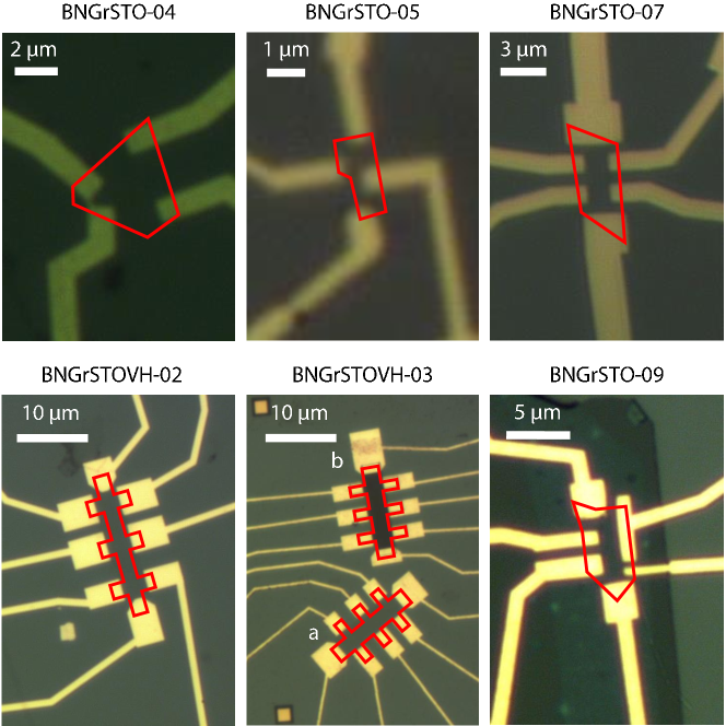
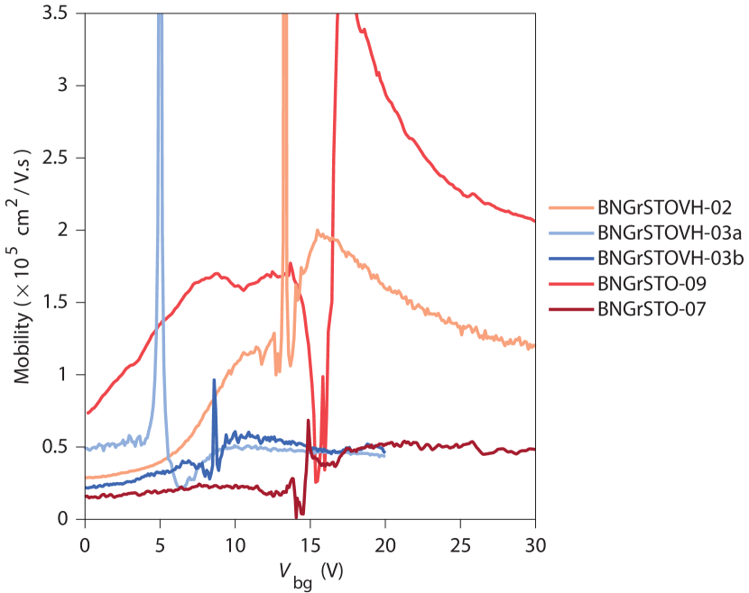
In this section we present a summary of the different samples studied. Optical images of the samples are shown in Fig. S1 and their geometry and transport characteristics are listed in Table S1. Thicknesses of the bottom hBN flakes for the samples showing an helical phase at low magnetic field vary between 1.6 nm and 5 nm. Graphene flake sizes vary from 1.6 m up to 15 m. The highest Hall mobility in our samples with thin hBN spacer reaches up to cm2/V.s for sample BNGrSTOVH-02, as shown in Fig. S2.
Moreover, a sample with a thick bottom hBN layer was measured to confirm the importance of the hBN spacer thickness. Transport measurements of this sample are shown in supplementary text section 6. A device with a Corbino geometry was also studied to investigate bulk transport and the presence of a bulk gap at charge neutrality. Details about its fabrication and transport measurements are presented in supplementary text section 5.
| Sample |
|
|
|
|
||||||||
| BNGrSTO-04 | 3 | 5 | ||||||||||
| BNGrSTO-05 | 4 | 3.3 | ||||||||||
| BNGrSTO-07 | 6 | 3.2 | ||||||||||
| BNGrSTOVH-02 | 8 | 5 | ||||||||||
| BNGrSTOVH-03a | 8 | 4 | ||||||||||
| BNGrSTOVH-03b | 8 | 4 | ||||||||||
| BNGrSTO-Corbino1 | 2 | 1.6 | / | |||||||||
| BNGrSTO-09 | 6 | 61 |
IV IV. Dielectric constant at T K
The doping of the hBN-encapsulated graphene flake with the application of a back-gate voltage is usually modeled by an equivalent plate capacitor. The corresponding capacitance is the sum of the two capacitances coming from the hBN spacer and the SrTiO3 (STO) substrate, such that:
| (2) |
where and are respectively the thicknesses of the SrTiO3 substrate and the hBN spacer and , , are respectively the relative dielectric constants of the SrTiO3 substrate, the hBN spacer and the overall system. Since , the resulting relative permittivity is:
| (3) |
At low temperature, the relative dielectric constant of the hBN spacer is . Thus with , we obtain . The gate capacitance is therefore mainly determined by the relative permittivity of SrTiO3 and one can assume that .
The dielectric constant measured for different Hall bars at K is shown in Fig. S3. is non-linear with the electric field and ranges from 5 000 to 35 000, coherent with the expected value for the dielectric constant of SrTiO3 at low temperature. One substrate even shows a surprisingly high dielectric constant reaching 70 000 at V.
V V. Helical edge transport in other devices
In this section we present transport measurements performed on additional samples displaying characteristic signatures of the ferromagnetic (F) phase with helical edge states.
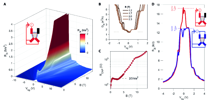
Figure S4 presents results of transport measurements for sample BNGrSTO-04, in the same fashion as in Fig. 2 of the main text. This sample is a Hall bar with 3 contacts (the lower two being shortcut), which leads to specific quantization values. As shown in Fig. S4A and B, the QSH plateau develops under a magnetic field between 1 T and 3 T. The resistance value reaches the expected value for helical edge transport in this contact configuration, that is, . In Fig. S4D we further show two different contact configurations with swapping contacts. In both cases, the resistance at charge neutrality reaches the expected value for helical transport indicated by the dotted red and blue lines.
Figure S5 presents the data obtained on sample BNGrSTO-05 equipped with four contacts. We observe a resistance plateau at charge neutrality between 1 T and 2.6 T (see Fig. S5B and C), consistent with helical edge transport.
In Figure S6 we present the evolution of the two-terminal resistance with respect to contact configuration for sample BNGrSTOVH-02, which is patterned in Hall bar geometry with eight contacts (see Fig. S1). As in Fig. 2 of the main text, the resistance in six different configurations reaches around charge neutrality the quantized value expected for helical edge transport.
Contrary to the sample BNGrSTO-07 presented in the main text, this sample was etched, so that the graphene edges are not native from the exfoliation but rough from plasma etching. This shows the independence of the F phase with respect to the edge roughness induced by plasma etching. The quantized value of is reached over the complete length of the Hall bar, achieving a combined length of 15m on each arm. Although the presence of floating contacts does not allow to draw conclusions on the coherence length, we can notice that disorder and edge roughness accumulated over m does not affect the quantization of the resistance in the F phase.
VI VI. Resistance quantization for different points of the (B,T) phase diagram
In this section we present the two-terminal resistance of sample BNGrSTO-07 measured at several temperatures and for different magnetic fields, for different contact configurations corresponding to the points marked by green and red stars in Fig. 4C of the main text. In Figure S7A the top row plots show the expected quantization of the resistance at charge neutrality for the three contact configurations shown in Fig. S7B. On the contrary, when passing the limit of the F phase as shown in Fig. 4C of the main text, all resistances increase beyond the expected helical value (see bottom row plots in Fig. S7A).
VII VII. Gap opening measured in Corbino geometry
Due to the presence of helical edge channels in the F phase, the existence of a bulk gap in the state can not be inferred directly from transport measurements in a Hall bar geometry. Therefore to show the existence of a bulk band-gap at , we designed a graphene device in a Corbino geometry. In this geometry, graphene is contacted in the middle of the flake, preventing any edge states from connecting the different contacts, and giving access to bulk transport via measurement of the two-probe resistance between contacts.
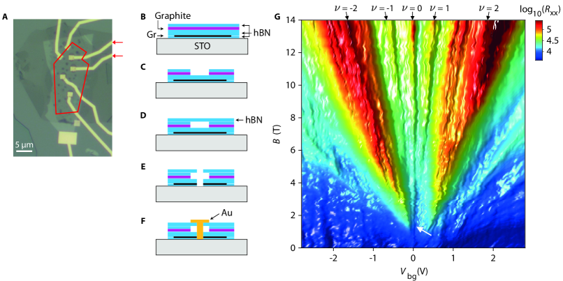
An optical picture of our Corbino geometry device is shown in Fig. S8A. The hBN/graphene/hBN stack was first placed on SrTiO3 substrate, then covered with a graphite/hBN layer (see Fig. S8B). The electrostatic screening of the graphite flake prevents the gold lines passing on the top of the heterostructure (see Fig. S8A) from doping locally the graphene sample, which could induce quantum Hall edge states connecting the inner contacts to the graphene edges Polshyn et al. (2018); Zeng et al. (2019). The graphite layer was then etched to drill holes that enable to access and contact the graphene (see Fig. S8C). A thin (nm) hBN flake was deposited on top of the etched holes (Fig. S8D), to prevent contacting the graphite layer with the metallic electrodes. Smaller holes in this last hBN flake and the graphene flake were then made in the middle of the first etched holes via an additional etching step (Fig. S8E). Finally, Cr/Au contacts were deposited in these holes to make edge contacts to the graphene (Fig. S8F).
The device was measured in two-terminal configuration between the two inner contacts indicated with the red arrows in Fig. S8A. Fig. S8G shows a colormap of the two-terminal resistance, with respect to back-gate voltage and magnetic field. We observe resistance peaks, appearing at T around charge neutrality, which disperse with magnetic field, analogous to what can be observed in a Landau fan diagram. Those insulating peaks indicate the opening of gaps in the density of states between Landau levels and their broken-symmetry states. The two main resistance peaks arising in red color correspond to the cyclotron gaps between the and Landau levels, similarly to what was already observed in high mobility graphene devices on SiO2 Polshyn et al. (2018); Zeng et al. (2019). Moreover, for T, three resistance peaks develop near charge neutrality in the zeroth Landau level between the two main resistance peaks. A first central peak, not dispersing in magnetic field, appears above T at charge neutrality, which corresponds to the gap of the state. Two additional satellites peaks appears above 5 T and correspond to the opening of the broken-symmetry states. Importantly, the gap at state appears for a field value virtually identical to the one where helical edge transport at charge neutrality sets in in the different samples. This bears out our conclusions of a F phase, gapped in the bulk and harboring helical edge channels, as the ground state of our screened graphene devices at charge neutrality.
VIII VIII. Activation gap at charge neutrality
We present in this section the Arrhenius plots that lead to the activation gaps displayed in Figure 4E of the main text.
Figure S9A shows the Arrhenius plot of the longitudinal four-terminal resistance measured in sample BNGrSTOVH-02, versus inverse temperature. This sample displays helical transport features (see Fig. S6). For T, we observe an activated temperature dependence of the resistance that we ascribe to the opening of a gap in the edge excitation spectrum. The -evolution of this gap is shown in Fig. 4E of the main text.
Figure S9B presents the Arrhenius plot of the longitudinal four-terminal resistance measured in sample BNGrSTO-09. In this sample, the hBN spacer layer is 61 nm thick and no helical edge transport is observed. We instead observe a strong insulating behaviour upon increasing magnetic field as seen on Fig. S10, which shows the evolution of the longitudinal four-terminal resistance for both samples (notice that for sample BNGrSTO-07 the contact configuration is different from the one of Figure 2 of the main text). It emphasizes the fundamental difference of the insulating behaviours between samples with thin hBN spacer and samples with thick hBN spacer. Above 4 T, the saturation of the measured resistance for the sample with a 61 nm spacer corresponds to the noise level of our current amplifier.
IX IX. Magnetic-field-dependent dielectric screening in graphene
on SrTiO3 substrate
In our van der Waals heterostructures, the dielectric screening in the graphene plane involves three different dielectric media : SrTiO3, hBN, vacuum (see Fig. S11A). The presence of two dielectric interfaces gives rise to an infinite number of image charges, and the resulting expression contains an infinite number of terms Barcellona et al. (2018). Since the top hBN layer is much thicker than the bottom one and thicker than the magnetic length, one can greatly simplify the formula by considering that the top hBN layer is infinitely thick. In this case, the Coulomb interaction is given by the simple expression Jackson (1975) :
| (4) |
where is the distance between the two electrons (or holes), is the thickness of the bottom hBN layer, is the dielectric constant of the SrTiO3 substrate, and the dielectric constant of the exfoliated top and bottom hBN flakes. The term in the parenthesis represents the additional screening brought by the SrTiO3 substrate and depends on the distance between the charge carriers (see Fig. S11B). For separations much larger than the thickness of the bottom hBN layer, the Coulomb interaction is strongly reduced by the huge dielectric constant of the substrate, but for an intermediate distance , the reduction is “only” by a factor 10.
In the quantum Hall regime, the distance between two electrons from the same Landau level is roughly given by the magnetic length (26 nm at 1 T). Replacing by in the parenthesis of expression (4) gives a screening factor which depends on the magnetic field. For a typical bottom hBN thickness of 4 nm in our heterostructures, the screening factor is about 0.008 at 1 T, 0.03 at 4 T, and 0.06 at 9 T. The characteristic Coulomb energy can be written as :
| (5) |
with the magnetic-field-dependent screening factor given by:
| (6) |
reinforces the dependence of (see Fig. S11C). As a result, the Coulomb energy varies much more with magnetic field with SrTiO3 substrate than with usual SiO2 substrates. The strong reduction of the Coulomb energy at low magnetic field makes it comparable to the Zeeman energy (see Fig. S11D).
X X. Temperature dependence of SrTiO3 dielectric constant
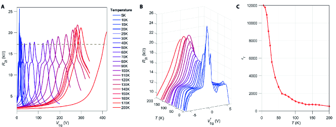
The dielectric constant of SrTiO3 exhibits a strong temperature dependence. It increases from a few hundreds at room temperature to about at low temperatures Sakudo and Unoki (1971). As a result, the back-gate voltage one must apply to have a specific carrier density significantly increases with temperature due to the decrease of with . Consequently, gate sweeps can only be performed up to a given temperature, fixed by the maximum back-gate voltage applicable. In our case, our maximal voltage limit of 420 V prevented us from carrying measurements above 200 K, where the charge neutrality point move to V at 14 T (see Fig. S12A).
To illustrate in more details this effect, we present in Fig. S12 the two-terminal resistance measured as a function of the back-gate voltage for sample BNGrSTO-07 at T, from which the data of Fig. 4C of the main text were extracted. As seen in Fig. S12A, the charge neutrality point moves to higher back-gate voltage values upon increasing due to the significant decrease of . Still, it is possible to rescale all back-gate voltage values into a equivalent back-gate voltage :
| (7) |
where is the temperature dependent dielectric constant of the back-gate electrode and is the temperature dependent back-gate voltage at charge neutrality. When rescaled, the curves at different temperatures superimpose, as shown in Fig. S12B, up to a temperature above which the helical quantization at charge neutrality is not observed anymore, and the plateaus start to be smeared.
We can furthermore use these data to estimate by calculating the difference in gate voltage between charge neutrality and the beginning of the plateau at T, which corresponds to a fixed carrier density, via the relation:
For our sample, we determined by Hall measurements at V and K.
The result of this analysis is shown in Fig. S12C. The dielectric constant rapidly decreases with temperature but is still close to 1000 at 200 K.