Carbon dimer defect as a source of the 4.1 eV luminescence in hexagonal boron nitride
Abstract
We propose that the carbon dimer defect in hexagonal boron nitride gives rise to the ubiquitous narrow luminescence band with a zero-phonon line of 4.08 eV (usually labeled the 4.1 eV band). Our first-principles calculations are based on hybrid density functionals that provide a reliable description of wide band-gap materials. The calculated zero-phonon line energy of 4.3 eV is close to the experimental value, and the deduced Huang-Rhys factor of , indicating modest electron-phonon coupling, falls within the experimental range. The optical transition occurs between two localized -type defects states, with a very short radiative lifetime of 1.2 nanoseconds, in very good accord with experiments.
Layered materials with inter-layer van der Waals (vdW) bonding have recently attracted a lot of interest due to their distinct chemical and physical properties Duong, Yun, and Lee (2017). Among this class of systems hexagonal boron nitride (hBN) stands out because of its large band gap of 6.08 eV Cassabois, Valvin, and Gil (2016). Advances in growth techniques have improved the materials quality Watanabe, Taniguchi, and Kanda (2004) and enabled the growth of single-layer hBN, opening up applications in electronic and optoelectronic devices. Currently hBN is mainly used in a passive role, for example as a substrate and/or insulating layer in electronic devices made of graphene and other vdW materials Duong, Yun, and Lee (2017), or as a dielectric for photonic crystal cavities Kim et al. (2018). However, hBN can also be used as an active optoelectronic material, e.g., as an electron-pumped ultraviolet (UV) laser Watanabe, Taniguchi, and Kanda (2004). The recent discovery Tran et al. (2016) that hBN can host bright and stable single-photon emitters in the visible spectral range has sparked huge interest in the application of hBN as a light source in quantum optics applications.
Photoluminescence (PL), cathodoluminescence (CL), and electroluminescence experiments dating back to the 1950s Larach and Shrader (1956) already revealed a strong emission band between 3.3 and 4.1 eV in bulk hBN. This near-UV emission was so prevalent in some early samples that the band gap of hBN was sometimes erroneously assumed to be just above 4 eV Solozhenko et al. (2001). However, more careful spectroscopic experiments Era, Minami, and Kuzuba (1981); Museur, Feldbach, and Kanaev (2008); Du et al. (2015) on better-quality material revealed that the 4 eV luminescence is defect-related and is composed of at least two bands with very distinct properties. One is a broad featureless band centered around 3.9 eV Museur, Feldbach, and Kanaev (2008). The other is a much narrower band with a clearly distinguishable zero-phonon line (ZPL) at 4.08 eV (typically called the 4.1 eV band in the literature) and which is accompanied by a few phonon replicas Era, Minami, and Kuzuba (1981); Museur, Feldbach, and Kanaev (2008); Du et al. (2015). The dimensionless Huang-Rhys parameter, which quantifies electron-phonon coupling during optical transitions Stoneham (2001), was estimated to fall in the range for this band Vokhmintsev, Weinstein, and Zamyatin (2019). The PL of this structured band appears when excitation energies exceed the ZPL of 4.1 eV. At variance, the broad 3.9 eV band appears only at excitation energies larger than 5.0 eV Museur, Feldbach, and Kanaev (2008). Furthermore, time-dependent luminescence associated with these bands possesses very distinct characteristics. The structured narrow band shows very fast single-exponential decay with a lifetime ns Era, Minami, and Kuzuba (1981); Museur, Feldbach, and Kanaev (2008), while the wide band exhibits multi-exponential dynamics with the slowest components having decay times of a few 100 ns Museur, Feldbach, and Kanaev (2008). All these results indicate a very distinct origin of the two bands, and from now on we will only discuss the structured 4.1 eV band.
Recently, single-photon emission associated with the 4.1 eV band has been reported Bourrellier et al. (2016). Fast electrons in a transmission electron microscope Meuret et al. (2015) were used to excite luminescence at K. Measurement of the second-order correlation function confirmed that photons originate at a single emitter. The lineshape and the lifetime Meuret et al. (2015) of the CL band were identical to those in ensemble measurements, confirming that in both experiments luminescence was caused by the same defect. These experiments have renewed the interest in the 4.1 eV band due to its potential use in quantum optics.
Despite the ubiquity of the 4.1 eV line, the microscopic nature of the defect that causes the luminescence is still not known. The intensity of the band increases drastically in both bulk crystals Era, Minami, and Kuzuba (1981) and epitaxial layers Uddin et al. (2017) when carbon is purposely introduced during growth. Therefore, the involvement of carbon has been naturally assumed Era, Minami, and Kuzuba (1981); Du et al. (2015). It has been suggested Katzir et al. (1975); Du et al. (2015); Uddin et al. (2017) that the 4.1 eV emission is caused by a transition from either a shallow donor (a so-called donor-acceptor-pair or DAP transition) or from the conduction band (free-to-bound transition) to the neutral carbon acceptor on the nitrogen site, C. There are strong arguments against these scenarios. First, the time dynamics of DAP and free-to-bound transitions are inconsistent with the measured lifetime of ns. For DAP transitions, the variation in donor-acceptor pair distances usually leads to marked non-exponential decay dynamics with very long tails Museur, Feldbach, and Kanaev (2008), at odds with the single-exponential decay of the 4.1 eV line Era, Minami, and Kuzuba (1981); Museur, Feldbach, and Kanaev (2008). Regarding radiative free-to-bound transitions, these occur on a millisecond time scale at typical excitation conditions (carrier densities cm3) Stoneham (2001), significantly slower than the dynamics of the 4.1 eV line. An additional argument comes from our recent first-principles study Weston et al. (2018), where the acceptor level of C was found to be at 2.9 eV above the valence band maximum (VBM). Since the band gap of hBN is 6.1 eV, DAP and free-to-bound transitions should therefore have energies smaller than 3.2 eV, i.e., they should not appear in the UV at all. The fast nanosecond radiative decay dynamics of the 4.1 eV line Era, Minami, and Kuzuba (1981); Meuret et al. (2015); Museur, Feldbach, and Kanaev (2008) indicates that this is a transition where the ground state and excited state are localized in close proximity, likely on the same defect. Recently, Korona and Chojecki Korona and Chojecki (2019) used quantum chemistry calculations to suggest that carbon clusters made from two to four atoms give luminescence in the range from 3.9 to 4.8 eV in monolayer hBN. However, different UV lines were not discriminated in that study, and neither the stability of clusters nor parameters (lifetime and electron-phonon coupling) of optical transitions were investigated.
In this Letter we use first-principles density functional theory to show that the complex, in which two carbon atoms substitute on nearest-neighbor sites in the hBN lattice, accounts for all known experimental facts about the 4.1 eV luminescence: the involvement of carbon, the energy of the transition, the very short radiative lifetime, and moderate electron-phonon coupling.
Our calculations are based on the hybrid density functional of Heyd, Scuseria, and Ernzerhof Heyd, Scuseria, and Ernzerhof (2003). In this approach, a fraction of screened Fock exchange is admixed to the short-range exchange potential described by the generalized gradient approximation of Perdew, Burke and Ernzerhof Perdew, Burke, and Ernzerhof (1996). We use , for which calculations yield a band gap of 6.42 eV, consistent with the experimental gapCassabois, Valvin, and Gil (2016) when zero-point renormalization due to electron-phonon interactions Antonius et al. (2015) is accounted for. We used the projector-augmented wave approach Blöchl (1994) with a plane-wave energy cutoff of 500 eV, and van der Waals interactions were included via the Grimme D3 empirical correction scheme Grimme (2006). With these settings the calculated lattice parameters of hBN ( Å and Å) and the enthalpy of formation for hBN (2.96 eV per formula unit) are in very good agreement with experimental values Tomaszkiewicz (2002). Defect calculations have been performed in orthorhombic supercells containing 240 atoms Weston et al. (2018) and with lattice vectors , , , where , , are vectors of the primitive hBN lattice. The Brillouin zone was sampled at the point. Ionic relaxation was carried out until Hellman-Feynman forces were less than 0.005 eV/Å. Calculations have been performed using the Vienna Ab-initio Simulation package (vasp) Kresse and Furthmüller (1996).
We start by calculating the formation energy Freysoldt et al. (2014) of the carbon dimer , which is given by:
| (1) | |||||
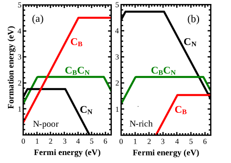
where is the total energy of the supercell containing one dimer, and is the total energy of a pristine supercell. and are chemical potentials of nitrogen and boron; , where is the total energy of bulk BN per formula unit. is the chemical potential of carbon, set to the per-atom energy of a diamond crystal. In Eq. (1) is the charge of the defect, and is the Fermi level, referenced to the VBM . is a finite-size electrostatic correction term Freysoldt, Neugebauer, and Van de Walle (2009). We note that the formation energy of the dimer does not depend on individual chemical potentials and , as . The calculated formation energy is shown in Fig. 1, together with formation energies of and defects Weston et al. (2018). For these two latter defects formation energies do depend on the chemical potentials of boron and nitrogen; only two limit cases are shown in Fig. 1. For N-rich conditions , half the energy of the N2 molecule; for B-rich (N-poor) conditions , the energy of the B atom in elemental boron.
We find that has three possible charge states, , , and (Fig. 1). The neutral charge state is the most stable one throughout most of the band gap, with a formation energy of 2.2 eV. As can be seen in Fig. 1, the formation energy of the dimer is not lower than those of simple substitutional defects for the two limiting cases of atomic chemical potentials. However, there is a wide range of chemical potentials () and Fermi levels for which is more stable than either or . In addition, if both and are present in the material (e.g., as a result of non-equilibrium growth), the formation of is expected. For example, when binds to to form ()0, an energy of 3.1 eV is released, indicating an exothermic reaction. We conclude that whenever carbon is present during the growth of hBN, should be a common defect.
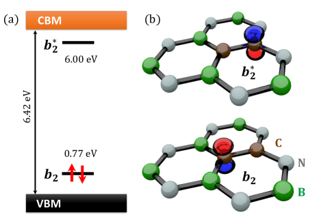
We now turn to electronic properties of the dimer. In the neutral state, which is the one we will consider here, the dimer is non-magnetic (). The Kohn-Sham electronic state diagram [Fig. 2(a)] shows that there are two defect states in the band gap. The lower-lying state is a orbital localized on the “acceptor” site , while the higher-lying state is a orbital on the “donor” site [Fig. 2(b)]. The defect geometry belongs to the point group, and both states can be labeled according to the irreducible representation . To distinguish the two states, we label the upper one .
In the ground state of the neutral dimer, the state is doubly occupied, while the state is empty, resulting in the electronic wave function (symbols without a bar are for spin-up electrons, symbols with a bar for spin-down). This is a singlet state . In the ground state the length of the CC, CN, and CB bonds are 1.361, 1.391, and 1.497 Å, respectively (cf. the nearest-neighbor distance of 1.435 Å in bulk hBN). The excited state is obtained when one electron is promoted to the state, yielding the wave function , also a state. We calculate the energy and the resulting geometry of the defect in the excited state using the so-called delta self-consistent field approach (SCF) Jones and Gunnarsson (1989) with constrained orbital occupations, as explained in the Supplementary Material. In the excited state there is a slight geometry rearrangement: the CC bond elongates by 7% to 1.456 Å, while CN and CB bond lengths change by less than 1.5% (to 1.372 and 1.499 Å, respectively).
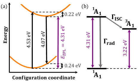
The calculated one-dimensional configuration coordinate diagram Stoneham (2001) is shown in Fig. 3(a). We obtain a ZPL energy of eV. The Franck-Condon shifts are eV in the excited state and eV in the ground state. To quantify electron-phonon coupling, we calculate Alkauskas et al. (2012) the Huang-Rhys factor , which is a measure of the average number of phonons emitted during the optical transitionStoneham (2001). We find an effective phonon frequency of meV, yielding the Huang-Rhys factor , which is consistent with the experimental estimate reported in Ref. Vokhmintsev, Weinstein, and Zamyatin, 2019. The Huang-Rhys factor is related to the Debye-Waller factor (the fraction of light emitted into the ZPL) via . Our calculated value of is smaller than the experimental value of reported in Ref. Vuong et al., 2016. However, note that due to the exponential dependence of on small errors in the latter can lead to large errors in the former.
Apart from the excited-state singlet , there is also a triplet state with configuration . is 3.22 eV above the ground state, i.e., 1.09 eV lower than the excited-state singlet due to the exchange interaction between the two electrons. The energy-level diagram of the neutral dimer is shown in Fig. 3(b).
The rate of the radiative transition between the two singlet states is given by (in SI units) Stoneham (2001):
| (2) |
Here is vacuum permittivity, is the refractive index of the host ( for energy eV Cappellini et al. (2001)), and is the computed transition dipole moment for the transition . Using the calculated value of eV, we obtain the rate s-1, corresponding to ns.
The transition is a strong dipole transition (so-called transition) with the polarization along the C–C bond. Experimental measurements of polarization would be really valuable but have not yet been performed so far. The calculated ns is in good agreement with the experimental value of ns Era, Minami, and Kuzuba (1981); Museur, Feldbach, and Kanaev (2008), but one should exercise caution comparing the two. The lifetime of the excited state is governed by two decay mechanisms [Fig. 3(b)]: the radiative transition to the ground state and the inter-system crossing (ISC) to the triplet state : . However, in the Supplementary Material we show that , and this justifies the comparison of the calculated rate with the measured one. Since , we also conclude that the quantum efficiency of the radiative transition is close to unity.
Our results show that the calculated optical properties of the defect are in very good agreement with the known properties of the 4.1 eV line. In fact, carbon dimers have been observed by annular dark field (ADF) electron microscopy in boron nitride monolayers Krivanek et al. (2010) exfoliated from bulk hBN. Carbon atoms have distinct intensity in ADF images, and this allowed a direct identification of C–C pairs Krivanek et al. (2010). This experimental proof of the existence of defects in bulk hBN inos in excellent agreement with our conclusions regarding the stability of carbon dimers.
In summary, we have reported the results of hybrid functional calculations for the carbon dimer in hexagonal boron nitride. Those calculations allow us to conclude that is the defect which is responsible for the 4.1 eV emission in hBN. The carbon dimer is expected to form whenever carbon is present during growth, explaining the observed correlation between the presence of carbon and the 4.1 eV line. The calculated zero-phonon line of the intra-defect optical transition of eV is close to the experimental value. Moreover, the theoretical Huang-Rhys factor of is consistent with the experimental estimate , and radiative lifetime ns is close to experimental value ns. Identification of the chemical nature of the defect will enable more controlled experiments involving the 4.1 eV line, in particular using the defect as a single photon emitter Bourrellier et al. (2016). Our analysis shows that the quantum efficiency of this emitter should be close to unity. Combined with a very short radiative lifetime this results in a very high photon yield. Together with a modest value of the Huang-Rhys factor (large weight of the ZPL) and a well-defined polarization axis, this makes the carbon dimer a very interesting quantum emitter in the near UV.
Supplementary Material
See Supplementary Material for the calculation of the excited state singlet and the inter-system crossing rate from the excited-state singlet to the state.
Acknowledgments
MMS and MM contributed equally to this work. We acknowledge useful discussions with Marcus W. Doherty, Lukas Razinkovas, and Mark Turiansky. AA was funded by the Grant No. 9.3.3.-LMT-K-712-14-0085 from the Research Council of Lithuania. MMS acknowledges funding from the European Union’s Horizon 2020 research and innovation programme under grant agreement No. 820394 (project Asteriqs). The research reported here was also partially supported by the National Science Foundation (NSF) through the Materials Research Science and Engineering Center at UC Santa Barbara, DMR-1720256 (Seed). Calculations were performed at the High Performance Computing Center “HPC Saulėtekis” in the Faculty of Physics, Vilnius University. Computational resources were also provided by the Extreme Science and Engineering Discovery Environment (XSEDE), supported by the NSF (ACI-1548562).
References
- Duong, Yun, and Lee (2017) D. L. Duong, S. J. Yun, and Y. H. Lee, ACS Nano 11, 11803 (2017).
- Cassabois, Valvin, and Gil (2016) G. Cassabois, P. Valvin, and B. Gil, Nature Photonics 10, 262 (2016).
- Watanabe, Taniguchi, and Kanda (2004) K. Watanabe, T. Taniguchi, and H. Kanda, Nature Materials 3, 404 (2004).
- Kim et al. (2018) S. Kim, J. E. Fröch, J. Christian, M. Straw, J. Bishop, D. Totonjian, K. Watanabe, T. Taniguchi, M. Toth, and I. Aharonovich, Nature Communications 9, 2623 (2018).
- Tran et al. (2016) T. T. Tran, K. Bray, M. J. Ford, M. Toth, and I. Aharonovich, Nature Nanotechnology 11, 37 (2016).
- Larach and Shrader (1956) S. Larach and R. E. Shrader, Physical Review 104, 68 (1956).
- Solozhenko et al. (2001) V. Solozhenko, A. Lazarenko, J.-P. Petitet, and A. Kanaev, Journal of Physics and Chemistry of Solids 62, 1331 (2001).
- Era, Minami, and Kuzuba (1981) K. Era, F. Minami, and T. Kuzuba, Journal of Luminescence 24, 71 (1981).
- Museur, Feldbach, and Kanaev (2008) L. Museur, E. Feldbach, and A. Kanaev, Physical Review B 78, 155204 (2008).
- Du et al. (2015) X. Du, J. Li, J. Lin, and H. Jiang, Applied Physics Letters 106, 021110 (2015).
- Stoneham (2001) A. M. Stoneham, Theory of defects in solids (Oxford University Press, 2001).
- Vokhmintsev, Weinstein, and Zamyatin (2019) A. Vokhmintsev, I. Weinstein, and D. Zamyatin, Journal of Luminescence 208, 363 (2019).
- Bourrellier et al. (2016) R. Bourrellier, S. Meuret, A. Tararan, O. Stéphan, M. Kociak, L. H. Tizei, and A. Zobelli, Nano Letters 16, 4317 (2016).
- Meuret et al. (2015) S. Meuret, L. H. G. Tizei, T. Cazimajou, R. Bourrellier, H. C. Chang, F. Treussart, and M. Kociak, Physical Review Letters 114, 197401 (2015).
- Uddin et al. (2017) M. Uddin, J. Li, J. Lin, and H. Jiang, Applied Physics Letters 110, 182107 (2017).
- Katzir et al. (1975) A. Katzir, J. Suss, A. Zunger, and A. Halperin, Physical Review B 11, 2370 (1975).
- Weston et al. (2018) L. Weston, D. Wickramaratne, M. Mackoit, A. Alkauskas, and C. G. Van de Walle, Physical Review B 97, 214104 (2018).
- Korona and Chojecki (2019) T. Korona and M. Chojecki, International Journal of Quantum Chemistry 119, e25925 (2019).
- Heyd, Scuseria, and Ernzerhof (2003) J. Heyd, G. E. Scuseria, and M. Ernzerhof, Journal of Chemical Physics 118, 8207 (2003).
- Perdew, Burke, and Ernzerhof (1996) J. P. Perdew, K. Burke, and M. Ernzerhof, Physical Review Letters 77, 3865 (1996).
- Antonius et al. (2015) G. Antonius, S. Poncé, E. Lantagne-Hurtubise, G. Auclair, X. Gonze, and M. Côté, Physical Review B 92, 085137 (2015).
- Blöchl (1994) P. E. Blöchl, Physical Review B 50, 17953 (1994).
- Grimme (2006) S. Grimme, Journal of Computational Chemistry 27, 1787 (2006).
- Tomaszkiewicz (2002) I. Tomaszkiewicz, Polish Journal of Chemistry 76, 891 (2002).
- Kresse and Furthmüller (1996) G. Kresse and J. Furthmüller, Physical Review B 54, 11169 (1996).
- Freysoldt et al. (2014) C. Freysoldt, B. Grabowski, T. Hickel, J. Neugebauer, G. Kresse, A. Janotti, and C. G. Van de Walle, Reviews of Modern Physics 86, 253 (2014).
- Freysoldt, Neugebauer, and Van de Walle (2009) C. Freysoldt, J. Neugebauer, and C. G. Van de Walle, Physical Review Letters 102, 016402 (2009).
- Jones and Gunnarsson (1989) R. O. Jones and O. Gunnarsson, Reviews of Modern Physics 61, 689 (1989).
- Alkauskas et al. (2012) A. Alkauskas, J. L. Lyons, D. Steiauf, and C. G. Van de Walle, Physical Review Letters 109, 267401 (2012).
- Vuong et al. (2016) T. Vuong, G. Cassabois, P. Valvin, A. Ouerghi, Y. Chassagneux, C. Voisin, and B. Gil, Physical Review Letters 117, 097402 (2016).
- Cappellini et al. (2001) G. Cappellini, G. Satta, M. Palummo, and G. Onida, Physical Review B 64, 035104 (2001).
- Krivanek et al. (2010) O. L. Krivanek, M. F. Chisholm, V. Nicolosi, T. J. Pennycook, G. J. Corbin, N. Dellby, M. F. Murfitt, C. S. Own, Z. S. Szilagyi, M. P. Oxley, S. T. Pantelides, and S. J. Pennycook, Nature 464, 571 (2010).