Stabilization of -Fe2O3 epitaxial layer on MgO(111)/GaN via an intermediate -phase
Abstract
In the present study we have demonstrated epitaxial stabilization of the metastable magnetically-hard -Fe2O3 phase on top of a thin MgO(111) buffer layer grown onto the GaN (0001) surface. The primary purpose to introduce a 4 nm-thick buffer layer of MgO in between Fe2O3 and GaN was to stop thermal migration of Ga into the iron oxide layer. Though such migration and successive formation of the orthorhombic GaFeO3 was supposed earlier to be a potential trigger of the nucleation of the isostructural -Fe2O3, the present work demonstrates that the growth of single crystalline uniform films of epsilon ferrite by pulsed laser deposition is possible even on the MgO capped GaN. The structural properties of the 60 nm thick Fe2O3 layer on MgO / GaN were probed by electron and x-ray diffraction, both suggesting that the growth of -Fe2O3 is preceded by formation of a thin layer of -Fe2O3. The presence of the magnetically hard epsilon ferrite was independently confirmed by temperature dependent magnetometry measurements. The depth-resolved x-ray and polarized neutron reflectometry reveal that the 10 nm iron oxide layer at the interface has a lower density and a higher magnetization than the main volume of the -Fe2O3 film. The density and magnetic moment depth profiles derived from fitting the reflectometry data are in a good agreement with the presence of the magnetically degraded -Fe2O3 transition layer between MgO and -Fe2O3. The natural occurrence of the interface between magnetoelectric - and spin caloritronic - iron oxide phases can enable further opportunities to design novel all-oxide-on-semiconductor devices.
The magnetic-on-semiconductor heterostructures attract a lot of interest nowadays due to the vast opportunities they provide for designing novel functional spintronic devices for magnetic memory applications and bio-inspired computing Prinz (1990); Ohno et al. (1999); Wolf et al. (2001); Yuasa et al. (2004); Kent and Worledge (2015); Grollier et al. (2016); Dieny and Chshiev (2017). Placing a multiferroic layer with controllable magnetization/polarization in contact with a semiconductor adds the functionality of controlling optical, electronic and magnetic properties of the heterostructure by applied voltage Scott (2007); Gajek et al. (2007); Ortega et al. (2015); Hu et al. (2017). One of the rare examples of material with spontaneous room-temperature magnetization and electric polarization is the metastable iron(III) oxide polymorph -Fe2O3 Gich et al. (2014); Ohkoshi et al. (2015); Katayama et al. (2017); Xu et al. (2018). Quite recently, the crystalline layers of -Fe2O3 have been successfully synthesized on a number of oxide substrates Gich et al. (2010, 2014); Thai et al. (2016); Hamasaki et al. (2017); Corbellini et al. (2017a); Viet et al. (2018) and GaN(0001) Suturin et al. (2018a). The structural and magnetic properties of the iron oxide films drastically depend on the composition of the neighboring buffer layer, the chosen substrate and the growth temperature. The feasibility to synthesize as much as four different iron oxide phases: -Fe2O3, Fe3O4, -Fe2O3 and -Fe2O3 on GaN(0001) by fine adjustment of growth parameters has been recently demonstrated Suturin et al. (2018a). It has been shown that stabilization of the -Fe2O3 phase requires elevated growth temperature that leads to formation of a few nanometer-thick Ga-rich magnetically soft transition layer at the interface between the iron oxide film and the GaN substrate Ukleev et al. (2018a). Later on, a very similar Ga/Fe substitution phenomena have been observed in yttrium iron garnet (YIG) films grown at above 700∘C onto a gadolinium gallium garnet (GGG) Suturin et al. (2018b). Although Ga-substituted epsilon-ferrite GaFeO3 is isostructural to -Fe2O3 Abrahams et al. (1965) and promotes further growth of the desired phase, its magnetic ordering temperature and coercivity field are somewhat lower than those of -Fe2O3 Katayama et al. (2017). This can potentially reduce the magnetoelectric and magnetooptical performance of the functional devices based on the -Fe2O3/ GaN heterostructures.
In the present study, we have successfully introduced an epitaxial MgO buffer between the -Fe2O3 and GaN layers to eliminate Ga migration into the iron oxide film. The resulting structural and magnetic properties of the fabricated heterostructure were probed by complementary x-ray diffraction (XRD), x-ray reflectometry (XRR), vibrating sample magnetometry (VSM), and polarized neutron reflectometry (PNR). An outcome of the epitaxial stabilization of -Fe2O3 on the MgO buffer is a technological advantage that provides further opportunities to integrate the promising epsilon ferrite into epitaxial Fe Goryunov et al. (1995); Klaua et al. (2001); Yuasa et al. (2004); Raanaei et al. (2008); Moubah et al. (2016), Fe3O4 Anderson et al. (1997); Margulies et al. (1997); Gao et al. (1997a); Kim et al. (1997); Voogt et al. (1999), -Fe2O3 Gao et al. (1997a, b); Kim et al. (1997) and -Fe2O3 Gao et al. (1997a); Voogt et al. (1999) heterostructures and superlattices grown on MgO substrates.
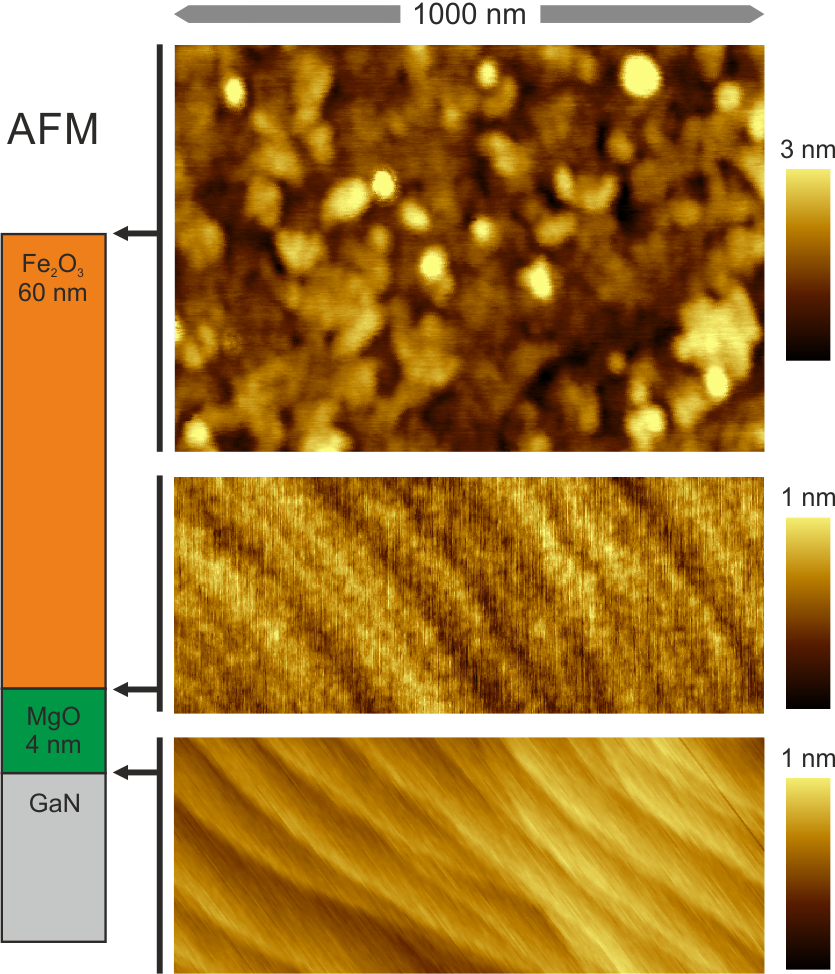
The substrates used in this work were commercial sapphire Al2O3 (0001) wafers with a 3 m-thick Ga terminated GaN (0001) layer grown on top by means of metalorganic vapour-phase epitaxy (MOVPE). The GaN surface showed a step-and-terrace surface morphology (Fig. 1) as confirmed by atomic force microscopy (AFM). The oxide layers were grown by pulsed laser deposition (PLD) from MgO and Fe2O3 targets ablated using a KrF laser. The crystallinity and epitaxial relations of the grown layers were controlled by in-situ high energy electron diffraction (RHEED) reciprocal space 3D mapping. With this technique Suturin et al. (2016) one obtains a 3D reciprocal space map from a sequence of conventional RHEED images taken during the azimuthal rotation of the sample. Thus obtained sequence of the closely spaced spherical cuts through the reciprocal space can be then compiled into a uniform 3D map and shown in the easy interpreted form of planar cuts and projections. The side cuts and plan views of the reciprocal space maps obtained at each growth stage are shown in the same scale in Fig. 2. The expected positions of the reciprocal lattice nodes are indicated with circles on the the left halves of the maps.
The 4 nm thick MgO layer was deposited onto GaN in 0.02 mbar of oxygen at the substrate temperature of 800∘ C. As confirmed by atomic force microscopy (Fig. 1), the MgO coverage on GaN is smooth and sufficiently uniform to serve as a diffusion barrier. The epitaxial relations extracted from RHEED are as follows: GaN(0001) MgO(111); GaN[1-10] MgO[11-2] (Fig. 2). The two possible MgO orientations arise due to the symmetry reduction occuring at the interface: from GaN(0001) C6 to MgO(111) C3. Reflections on the RHEED map of MgO are streaky corresponding to the semi-flat surface.
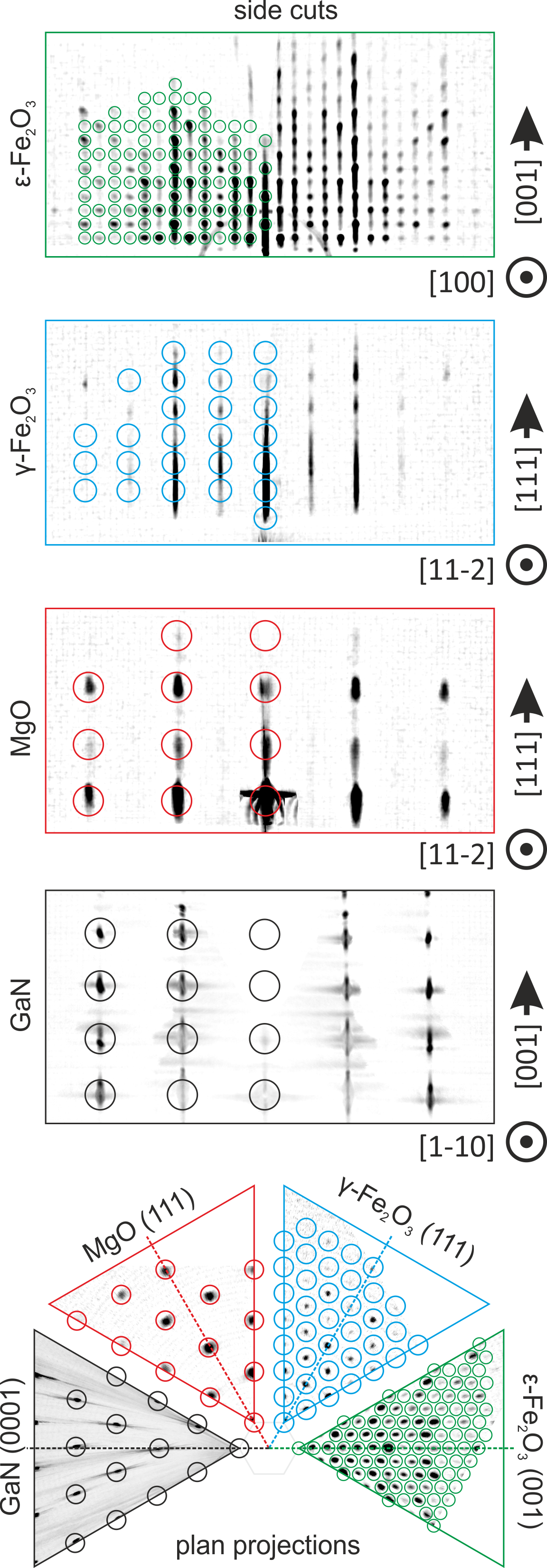
A 60 nm thick iron oxide layer was grown onto the surface of MgO(111) in 0.2 mbar of oxygen at the substrate temperature of 800∘ C following the approach described in our previous report Suturin et al. (2018a). It was discovered that unlike when grown directly on GaN, the iron oxide layer on MgO nucleates in gamma rather than in epsilon phase. Upon deposition of 3-5 nm of iron oxide, the RHEED reciprocal space maps start showing a distinct pattern of streaks characteristic for the spinel -Fe2O3 lattice (Fig. 2) oriented with the [111] axis perpendicular to the surface and the [11-2] axis parallel to MgO [11-2] and GaN[1-10]. The diffraction map remains streaky corresponding to the still flat surface.
The preference of the -Fe2O3 over -Fe2O3 is naturally related to the cubic symmetry of both lattices. The phase choice mechanisms for the Fe2O3 / MgO(111) system might be similar to those of the Fe2O3 / MgO (001) system where -Fe2O3 is known to be the dominant phase Gao et al. (1997a); Huang et al. (2013); Sun et al. (2014). It is noteworthy that a thin -like transition layer was also observed during the nucleation of - and -Fe2O3 directly on GaN Suturin et al. (2018a). Though the diffraction patterns of that layer bore resemblance to FeO, the spacing between the adjacent (111) layers of oxygen was very similar to -Fe2O3.
When the total thickness of the iron oxide reaches about 10 nm, the streak pattern gets gradually replaced by the streak pattern which is an unmistakable fingerprint of the -Fe2O3 phase. This pattern persists until the growth is stopped at 60 nm of the iron oxide total thickness (Fig. 2). The pattern is dotty rather than streaky in agreement with the few nm surface roughness measured by AFM (Fig. 1). The -Fe2O3 lattice is oriented with the polar [001] axis perpendicular to the surface and the easy magnetization [100] axis parallel to the one of the three equivalent GaN [1-10] in-plane directions resulting in three crystallographic domains at to each other. It is essential that the growth temperature at this stage is no less than 800∘C otherwise nucleation of -Fe2O3 phase does not occur.
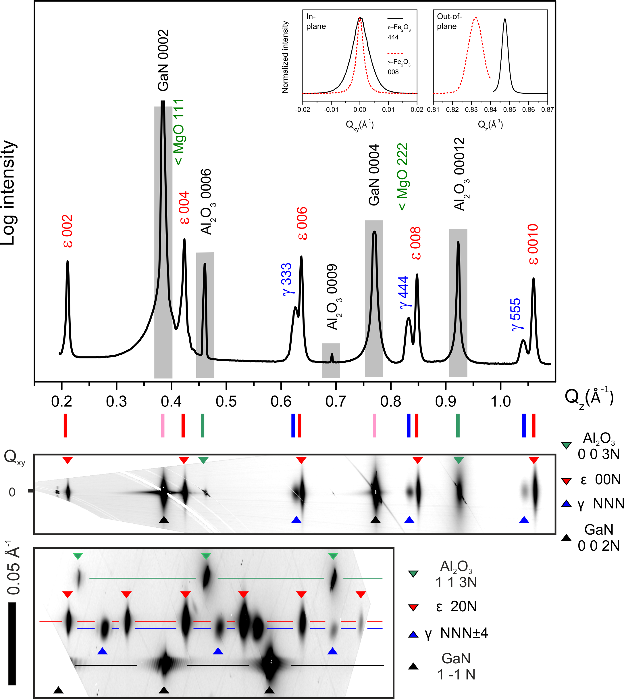
To accurately study the crystal structure of the film volume we have applied X-ray diffraction in addition to the surface sensitive RHEED. The XRD measurements were carried out at the BL-3A beamline, KEK Photon Factory (Tsukuba, Japan). The 3D reciprocal space maps were compiled from a series of diffraction patterns taken with a Pilatus 100K two-dimensional detector during a multi-angle rotation performed on a standard 4-circle Euler diffractometer. The linear and planar cuts through the 3D maps obtained across the reciprocal space specular region are shown in Fig. 3. The series of -Fe2O3 002N and -Fe2O3 111N reflections are easily identifiable in addition to the reflections of the underlying Al2O3 and GaN. We do not observe distinctly the reflections of MgO as they considerably overlap with those of -Fe2O3. Moreover the MgO layer is 15 times thinner than Fe2O3 and has about 1.5 times lower scattering length density for x-rays.
The derived out-of-plane lattice constant of epsilon ferrite Å is in agreement with our earlier studies of -Fe2O3 / GaN Suturin et al. (2018a). The (111) interplane distance in -Fe2O3 is in agreement with the bulk lattice constant of -Fe2O3 Å. The in-plane lattice arrangement becomes clear from the analysis of the reciprocal space region containing the off-specular -Fe2O3 20N reflections. The -Fe2O3 lattice shows a 1% in-plane expansion towards Å and Å. The -Fe2O3 lattice shows a 1.5 % lattice expansion towards the equivalent cubic lattice constant of Å. The in-plane expansion is not surprising taking into account the fact that the in-plane periodicity in GaN is about 8.5% larger than in Fe2O3 Suturin et al. (2018a). The observed in-plane and out-of-plane reflection widths may be used to judge on the strain relaxation and minimal crystallographic domain size in the grown films. The strain relaxation if present would involve a distribution of lattice parameters in the system and would cause reflection broadening that is proportional to the magnitude of the wave vector . Even if such a broadening is present in our system, it is below the experimental resolution as all the observed reflections are of the same shape and width. Such effect can be attributed to the finite size of the coherent crystallographic domains within the crystal lattice and is typical for the nanostructured samples. Measuring the in-plane and out-of-plane reflection widths (see the insets in Fig. 3) one can conclude that the minimal coherent domains of -Fe2O3 are shaped as (widthheight) 14 nm 35 nm columns (in agreement with Ref. Ukleev et al. (2018a)) while those of -Fe2O3 look like 33 nm 10 nm disks. The reduced coherent thickness of -Fe2O3 film suggests that a transition layer with a mixed lattice structure exist at the -Fe2O3/-Fe2O3 interface. The lateral coherence between the the adjacent nucleation sites is substantially reduced because the surface cell of the iron oxides is larger than that of MgO. Compared to -Fe2O3 the coherent domain of -Fe2O3 is smaller because of the larger surface cell and the lack of the C3 symmetry. Thus the antiphase boundaries are formed more frequently in -Fe2O3.
The magnetometry measurements were carried out using a Quantum Design PPMS vibrating-sample magnetometer (VSM). The magnetic field was applied in the sample plane along the [100] easy magnetization axis of one of the three -Fe2O3 domains. Fig. 4 shows the hysteresis loops measured in the temperature range of 5-400 K and corrected for the linear diamagnetic contribution of the substrate. The observed values of saturation magnetization were about 130 emu/cm3 at K and 100 emu/cm3 at K which is consistent with what was reported for -Fe2O3 nanoparticles Jin et al. (2004) and -Fe2O3 thin film grown on SrTiO3 (STO) Gich et al. (2014), YSZ Corbellini et al. (2017a); Knížek et al. (2018) and GaNUkleev et al. (2018a), and predicted from ab-initio calculations Xu et al. (2018).
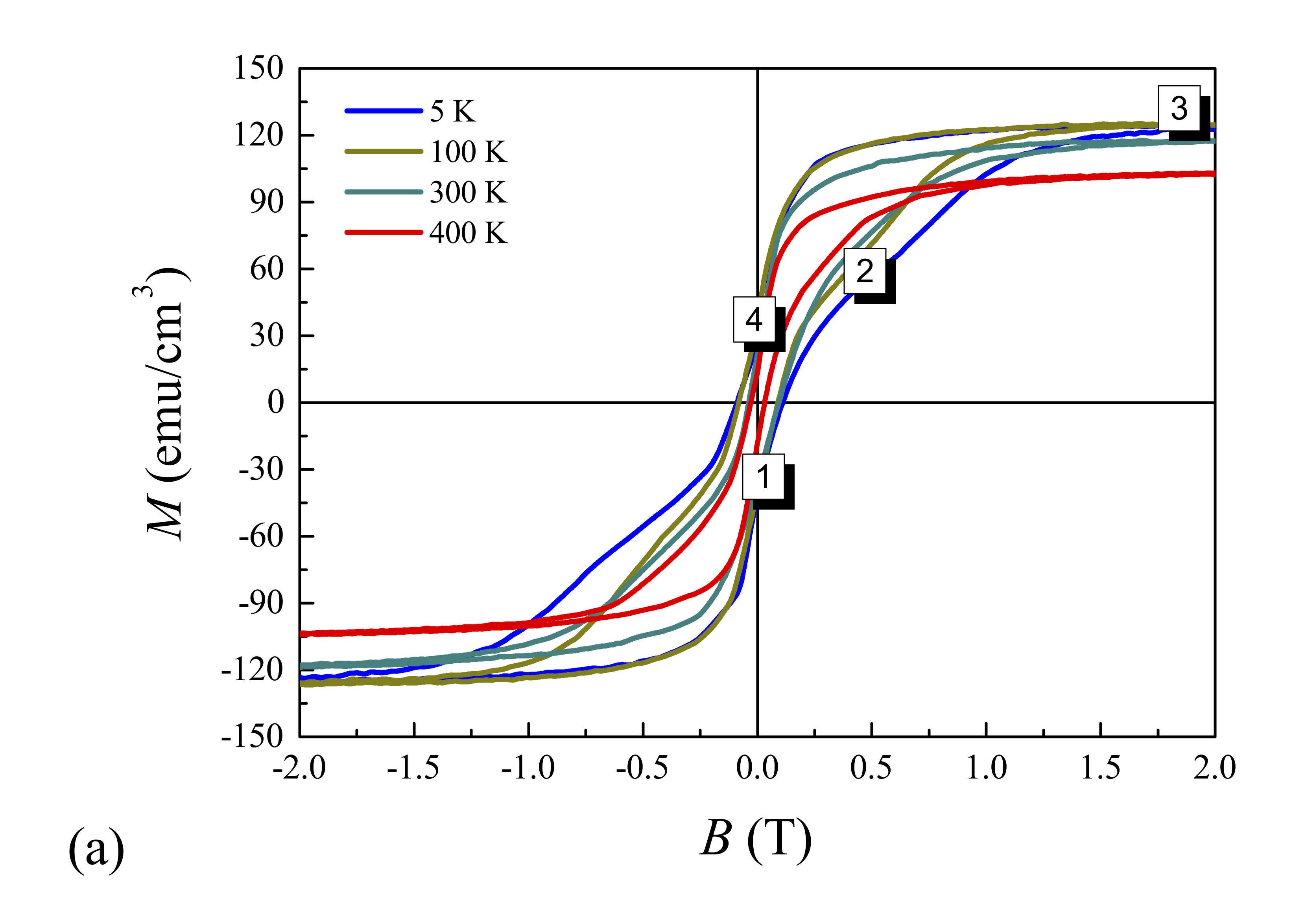
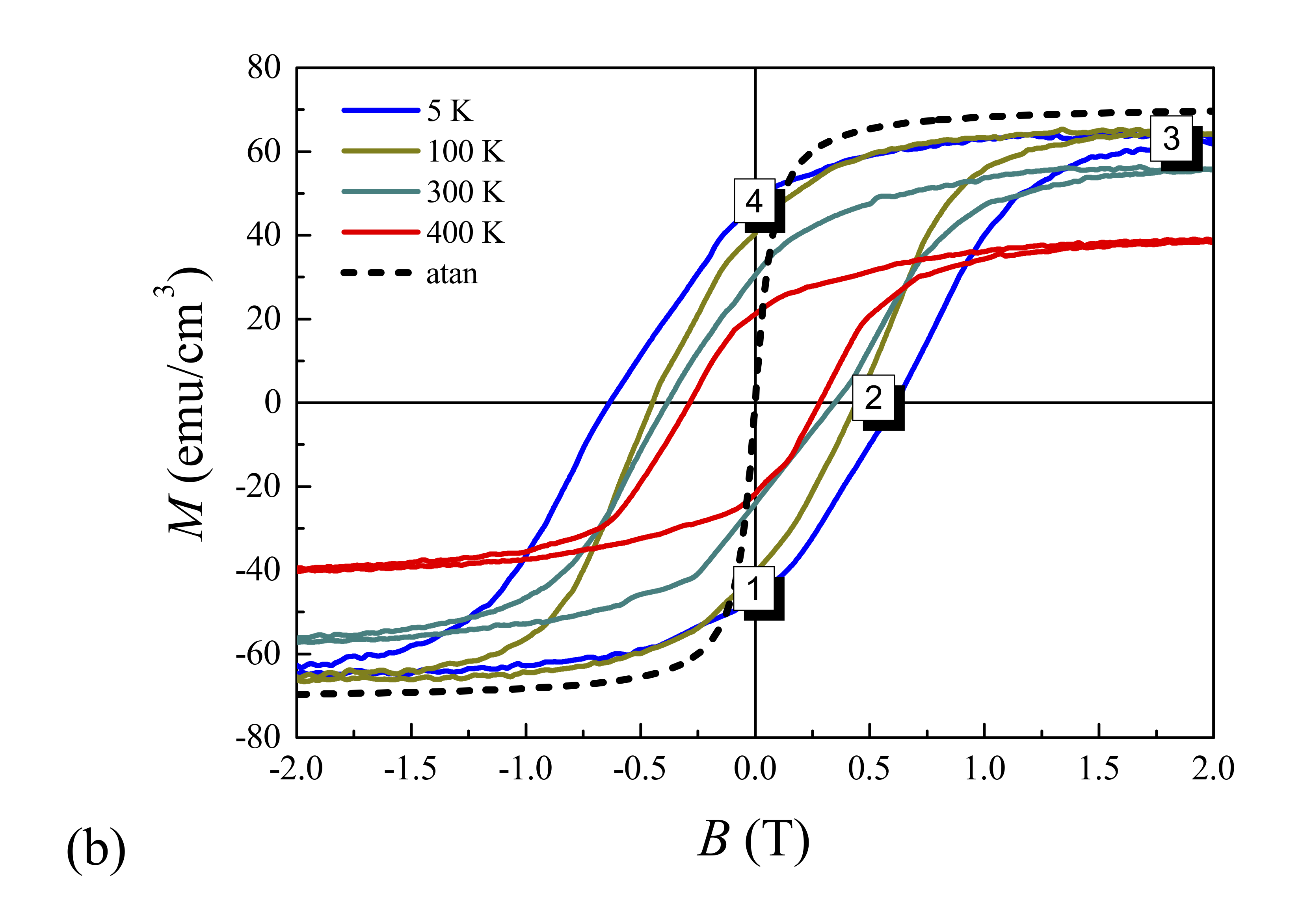
The wasp-waist magnetization loops shown in Fig. 4a are typical for -Fe2O3 films and nanoparticles and can be qualitatively decomposed to hard and soft component loops (Fig. 4b) by subtracting arctan(/) function with temperature-independent emu/cm3 and = 62 mT. These parameters were unambiguously derived from manual optimization aimed at making the remaining hard component smooth and monotonous in the vicinity of zero magnetic field.
The value of emu/cm3 observed for the soft magnetic component is in general agreement with the presence of -Fe2O3 sublayer buried below the main layer of -Fe2O3 as observed by XRD, RHEED and PNR. The magnetization plotted in Fig. 4b is normalized to the total film thickness of 70 nm. Taking into account the reported values of =300-400 emu/cm3 for -Fe2O3 / MgO, the soft loop can be attributed to a layer of -Fe2O3 having thickness of 12-14 nm. This is comparable though slightly higher than the thickness estimated from RHEED and PNR (see the details below).
The hard component hysteresis loops show a large saturation field of 1.2-1.8 T characteristic of -Fe2O3. The coercive field gradually increases as the sample is cooled down - from 0.27 T at 400 K to 0.66 T at 5 K. The loop shape is typical for the system with three uniaxial domains at 120 deg to each other. At saturation the magnetization is collinear to the field in all three domains . From saturation to zero field the magnetization gradually decreases to as the the magnetization in the two non collinear domains returns to the equilibrium state at 120 deg to the field. From this state the magnetization reversal is gradually completed towards the negative saturation. Notably, the magnetic phase transition to an incommensurate state that is often observed in -Fe2O3 nanoparticles, as dramatic shrinkage of the loop at K Gich et al. (2006); Tseng et al. (2009); García-Muñoz et al. (2017); Ohkoshi et al. (2017), has not been observed in -Fe2O3 films - neither on GaN nor on the other substrates. The absence of a sharp phase transition in films can be caused by the variation of the magnetic properties across the film depth. Thus, a temperature-dependent investigation of the depth resolved magnetic structure of -Fe2O3 films by neutron or resonant x-ray diffraction is highly desired to address this issue.
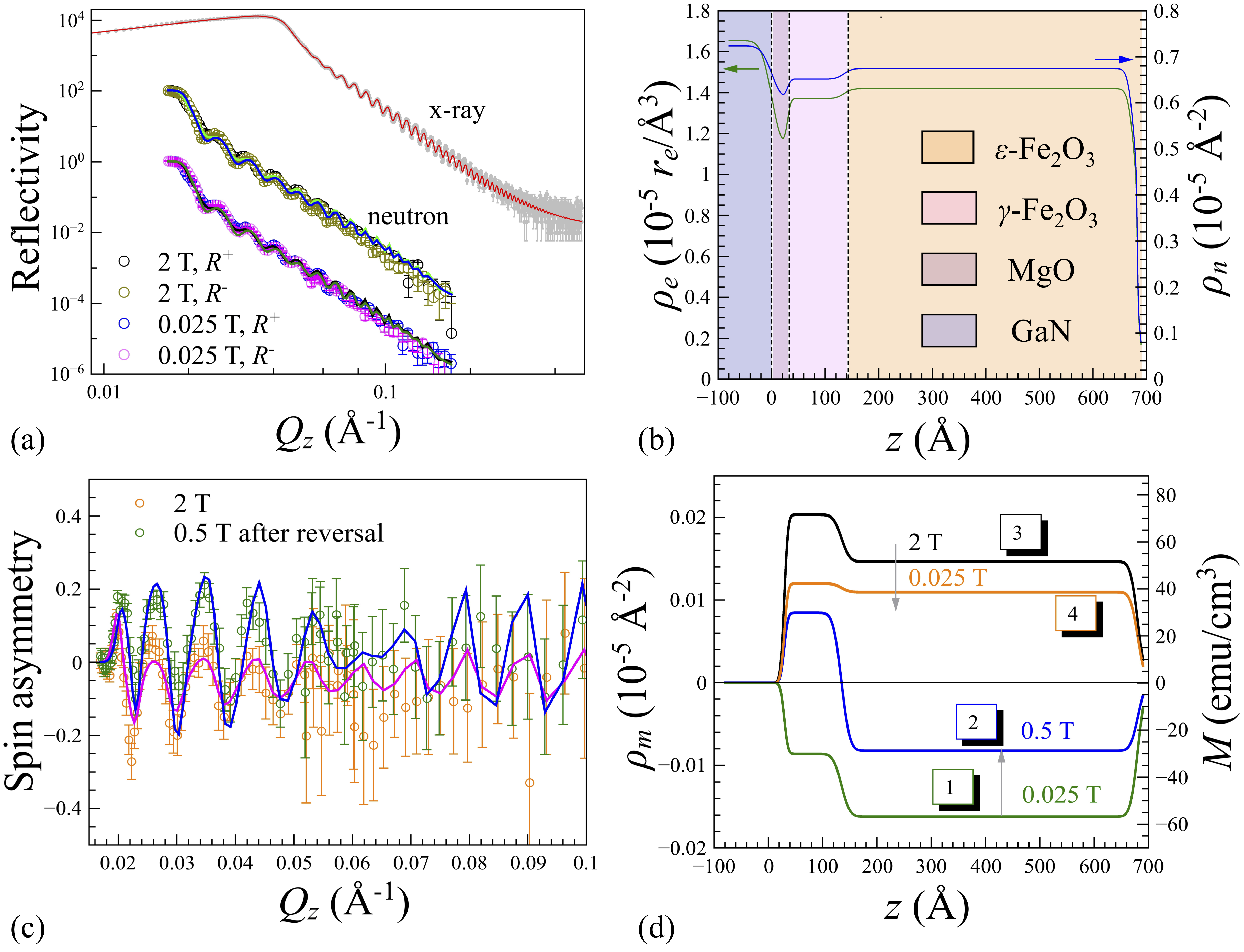
The XRR measurement was performed on the Panalytical X’Pert PRO x-ray diffractometer at room temperature using Cu (1.5406 Å) radiation to determine the electron scattering length density (SLD) profile of the film as a function of distance from the GaN surface . The specular reflectance was measured in the range of incident angles between 0.5 to 3.5 degrees covering the range from 0.075 to 0.5 Å-1.
The neutron reflectometry experiments were performed at the D17 setup Saerbeck et al. (2018); Ukleev et al. (2018b) (ILL, Grenoble, France) in polarized time-of-flight mode. Sample temperature and magnetic field were controlled by an Oxford Instruments 7 T vertical field cryomagnet equipped with single-crystalline sapphire windows. Neutrons with wavelengths of Å were used to ensure the constant polarization of . Three different incident angles (0.8, 1.5 and 3.7 degrees) were chosen to access the range from 0.017 to 0.17 Å-1. Intensity of the reflected beam was collected by two-dimensional 3He position-sensitive detector. The data was integrated using a method taking into account the sample curvature or beam divergence Saerbeck et al. (2018); Cubitt et al. (2015). Non-spin-flip reflectivities and , where +(-) denotes the incident neutron spin alignment parallel (antiparallel) to the direction of applied magnetic field, were acquired without polarization analysis. The detailed description of the reflectometry techniques can be found elsewhere Ankner and Felcher (1999); Zabel et al. (2008).
Figure 5a shows x-ray reflectivity (room temperature) and neutron reflectivity ( K) curves plotted as a function of momentum transfer . The neutron reflectivity curves were measured at the characteristic characteristic points of the loop marked as () in Fig.4. The PNR curves shown in Fig. 5a are measured in applied magnetic fields of T (state 1 in remanence) and T (state 3 in saturation). The XRR and PNR curves were simultaneously fitted using GenX software Björck and Andersson (2007). The simplest model, for which the fitting routine converges, corresponds to a stack consisting of the GaN substrate, the MgO buffer, the transition iron oxide layer with an unspecified density and the main -Fe2O3 layer. The depth-profiles of the x-ray () and nuclear neutron () scattering length densities (SLDs) extracted from the refined model are shown in Fig. 5b. The profiles reflect the chemical composition and density of the layers as well as the structural roughness of the interfaces. The root mean square (RMS) roughness of all the interfaces is below 15 Å. Notably, we observe the transition layer at the iron oxide/MgO interface with thickness of Å and reduced x-ray and neutron nuclear SLDs compared to the main -Fe2O3 volume of the film. This looks natural as -Fe2O3 having the same chemical formula as -Fe2O3 is by 3.4 % less dense due to the presence of iron vacancies in the inverted spinel structure. The comparably low SLD of the MgO layer gives a few nm wide reduction of and located on the SLD profile at .
The magnetization profile of the heterostructure is encoded in the dependence of the spin-asymmetry ratio (-)/(+) on . Fitting it against the model gives the depth profile of the magnetic contribution to the neutron SLD (Å-2) which can be converted to magnetization (emu/cm3) using the following formula: Zhu (2005). The measured and fitted spin-asymmetry ratios are shown in Fig. 5c for the two magnetic states 2 and 3 on the lower branch of the hysteresis loop (see Fig. 4): with partially switched magnetization ( T) and in full saturation ( T). The fitted model suggests that the iron oxide film is divided into two magnetically different sub-systems: the main -Fe2O3 layer with a saturation magnetization of emu/cm3 and an interfacial layer with emu/cm3 (Fig. 5d). Using the PNR data obtained at 5 K we are able to track the magnetization behavior of individual sublayers as the system is magnetized from the negative remanence (state 1) to full saturation (state 3) and back to the positive remanence (state 4). As shown in (Fig. 5d) the magnetization of the softer interface layer is switched between T (state 1) and T (state 2) and reaches saturation of 70 emu/cm3 at T. The magnetization of the much harder -Fe2O3 layer switches somewhere between T (state 2) and T (state 3). As the magnetically hard component of the hysteresis loop is not completely closed in the maximum applied positive of 2 T (Fig. 4b), the PNR curves measured at T (state 3) and T (state 4) belong to the minor branch of the hysteresis. Magnetization of 56 emu/cm3 is found at T, which is slightly smaller that the saturation moment. Going back to positive remanence of the minor loop (state 4), the magnetization of both interface and bulk layers start slowly decreasing (faster for the interface layer).
Sequential switching of interface - and main - layers in principle reflects a step-like shape of the hysteresis loops observed by VSM magnetometry (Fig. 4). It must be noted that the maximum magnetization for -Fe2O3 layer derived from PNR is about twice lower than the highest reported values for -Fe2O3 but in good agreement with the maximum magnetization observed in the decomposed VSM loop shown in Fig. 4b. The maximum magnetization of the -Fe2O3 layer derived from PNR is about 5 times lower than the expected 300-400 emu/cm3 reported for -Fe2O3/MgO layers Gao et al. (1997a); Huang et al. (2013); Sun et al. (2014), and cannot completely explain the soft-magnetic component observed by VSM. Magnetic degradation of the transition -Fe2O3 layer can be possibly explained by the size effect Orna et al. (2010), epitaxial strain Yang et al. (2010); Bertinshaw et al. (2014); Gibert et al. (2015) or large number of the antiphase boundaries Rigato et al. (2007); Ramos et al. (2009) between the nano-columns in the plane of the layer and at the interface with main -Fe2O3 film.
The much higher magnetization of the soft magnetic component observed in VSM suggests that another soft magnetic phase is likely present in the sample that cannot be distinguished in the PNR experiment. Similar effect was also observed in -Fe2O3 grown directly on GaN Ukleev et al. (2018a). The most plausible candidates are homogeneously distributed minor fractions of polycrystalline -Fe2O3 and Fe3O4 Jin et al. (2005); López-Sánchez et al. (2016); Corbellini et al. (2017b) not pronounced in XRD data. Again, one must also take into account the columnar structure of the -Fe2O3 films containing considerable concentration of the antiphase boundaries. As was pointed out in Ref. Sofin et al. (2011) the antiphase boundaries in iron oxides may account for the soft magnetic behavior. The magnetic moments located in minor phase fractions of small volume, or at the antiphase boundaries in the sample plane that cannot be resolved with PNR, which is a laterally averaging technique, because the disordered moments at boundaries and minor phase fractions are highly diluted, but integrated into the magnetization measured by VSM. We suggest that the deposition of small (m-scale) iron particulates ejected from the PLD target is the most plausible scenario, that have been also observed for other PLD films Haindl et al. (2016); Zhai et al. (2018); Grant-Jacob et al. (2018).
In conclusion, we have demonstrated the possibility to epitaxially grow single crystal -Fe2O3 thin film on MgO(111) surface by pulsed laser deposition. In contrast to the previously investigated non-buffered -Fe2O3/GaN(0001) system, where the interfacial GaFeO3 magnetically degraded layer was reported to form due to Ga diffusionUkleev et al. (2018a) from GaN, the -Fe2O3 / MgO / GaN system has advantage of exploiting the diffusion blocking MgO barrier. Though formation of the orthorhombic GaFeO3 was supposed earlier to be a potential trigger of the nucleation of the isostructural -Fe2O3, the present work demonstrates that the growth of single crystalline uniform films of epsilon ferrite by pulsed laser deposition is possible even without the aid of Ga. Still the aid of Ga seems important as on GaN the -Fe2O3 layer could be nucleated with a transition layer of few angstrom thickness while on MgO the growth of -Fe2O3 film is preceded by nucleation of a 10 nm thick layer of another iron oxide phase. A complimentary combination of electron and x-ray diffraction, x-ray reflectometry and polarized neutron reflectometry techniques allowed unambiguous identification of this phase as () cubic -Fe2O3. This phase is known to show magnetoelectric functionality Cheng et al. (2016) and spin Seebeck effect Jiménez-Cavero et al. (2017) and can enable further opportunities to design the novel all-oxide heterostructure magnetoelectric and spin caloritronic devices.
We are grateful to Institut Laue-Langevin for provided neutron and x-ray reflectometry beamtime (proposal No.: 5-54-244 Ukleev et al. (2018b)). Synchrotron x-ray diffraction experiment was performed at KEK Photon Factory as a part of the proposal No. 2018G688. We thank Dr. Tian Shang for the assistance with magnetization measurements. The part of the study related to PNR and XRR was partially supported by SNF Sinergia CRSII5-171003 NanoSkyrmionics. The part of the study related to growth technology and diffraction studies was supported by Russian Foundation for Basic Research grant №18-02-00789. The open access fee was covered by FILL2030, a European Union project within the European Commission’s Horizon 2020 Research and Innovation programme under grant agreement No. 731096.
References
- Prinz (1990) G. A. Prinz, Science 250, 1092 (1990).
- Ohno et al. (1999) Y. Ohno, D. Young, B. Beschoten, F. Matsukura, H. Ohno, and D. Awschalom, Nature 402, 790 (1999).
- Wolf et al. (2001) S. Wolf, D. Awschalom, R. Buhrman, J. Daughton, S. Von Molnar, M. Roukes, A. Y. Chtchelkanova, and D. Treger, Science 294, 1488 (2001).
- Yuasa et al. (2004) S. Yuasa, T. Nagahama, A. Fukushima, Y. Suzuki, and K. Ando, Nature Materials 3, 868 (2004).
- Kent and Worledge (2015) A. D. Kent and D. C. Worledge, Nature Nanotechnology 10, 187 (2015).
- Grollier et al. (2016) J. Grollier, D. Querlioz, and M. D. Stiles, Proceedings of the IEEE 104, 2024 (2016).
- Dieny and Chshiev (2017) B. Dieny and M. Chshiev, Reviews of Modern Physics 89, 025008 (2017).
- Scott (2007) J. Scott, Nature Materials 6, 256 (2007).
- Gajek et al. (2007) M. Gajek, M. Bibes, S. Fusil, K. Bouzehouane, J. Fontcuberta, A. Barthélémy, and A. Fert, Nature Materials 6, 296 (2007).
- Ortega et al. (2015) N. Ortega, A. Kumar, J. Scott, and R. S. Katiyar, Journal of Physics: Condensed Matter 27, 504002 (2015).
- Hu et al. (2017) J.-M. Hu, C.-G. Duan, C.-W. Nan, and L.-Q. Chen, NPJ Computational Materials 3, 18 (2017).
- Gich et al. (2014) M. Gich, I. Fina, A. Morelli, F. Sánchez, M. Alexe, J. Gàzquez, J. Fontcuberta, and A. Roig, Advanced Materials 26, 4645 (2014).
- Ohkoshi et al. (2015) S.-I. Ohkoshi, A. Namai, K. Imoto, M. Yoshikiyo, W. Tarora, K. Nakagawa, M. Komine, Y. Miyamoto, T. Nasu, S. Oka, and H. Tokoro, Scientific Reports 5, 14414 (2015).
- Katayama et al. (2017) T. Katayama, S. Yasui, Y. Hamasaki, T. Osakabe, and M. Itoh, Journal of Materials Chemistry C 5, 12597 (2017).
- Xu et al. (2018) K. Xu, J. Feng, Z. Liu, and H. Xiang, Physical Review Applied 9, 044011 (2018).
- Gich et al. (2010) M. Gich, J. Gazquez, A. Roig, A. Crespi, J. Fontcuberta, J. Idrobo, S. Pennycook, M. Varela, V. Skumryev, and M. Varela, Applied Physics Letters 96, 112508 (2010).
- Thai et al. (2016) T. M. N. Thai, D. T. Nguyen, N.-S. Lee, J.-S. Rhyee, J. Song, and H.-J. Kim, Journal of Applied Physics 120, 185304 (2016).
- Hamasaki et al. (2017) Y. Hamasaki, T. Shimizu, S. Yasui, T. Shiraishi, A. Akama, T. Kiguchi, T. Taniyama, and M. Itoh, Journal of Applied Physics 122, 015301 (2017).
- Corbellini et al. (2017a) L. Corbellini, C. Lacroix, C. Harnagea, A. Korinek, G. A. Botton, D. Ménard, and A. Pignolet, Scientific Reports 7 (2017a).
- Viet et al. (2018) V. Q. Viet, S. Y. Adeyemi, W. H. Son, J.-S. Rhyee, N.-S. Lee, and H.-J. Kim, Crystal Growth & Design 18, 3544 (2018).
- Suturin et al. (2018a) S. Suturin, A. Korovin, S. Gastev, M. Volkov, A. Sitnikova, D. Kirilenko, M. Tabuchi, and N. Sokolov, Physical Review Materials 2, 073403 (2018a).
- Ukleev et al. (2018a) V. Ukleev, S. Suturin, T. Nakajima, T.-h. Arima, T. Saerbeck, T. Hanashima, A. Sitnikova, D. Kirilenko, N. Yakovlev, and N. Sokolov, Scientific Reports 8, 8741 (2018a).
- Suturin et al. (2018b) S. Suturin, A. Korovin, V. Bursian, L. Lutsev, V. Bourobina, N. Yakovlev, M. Montecchi, L. Pasquali, V. Ukleev, A. Vorobiev, A. Devishvili, and N. Sokolov, Physical Review Materials 2, 104404 (2018b).
- Abrahams et al. (1965) S. Abrahams, J. Reddy, and J. Bernstein, The Journal of Chemical Physics 42, 3957 (1965).
- Goryunov et al. (1995) Y. V. Goryunov, N. Garif’yanov, G. Khaliullin, I. Garifullin, L. Tagirov, F. Schreiber, T. Mühge, and H. Zabel, Physical Review B 52, 13450 (1995).
- Klaua et al. (2001) M. Klaua, D. Ullmann, J. Barthel, W. Wulfhekel, J. Kirschner, R. Urban, T. L. Monchesky, A. Enders, J. F. Cochran, and B. Heinrich, Physical Review B 64, 134411 (2001).
- Raanaei et al. (2008) H. Raanaei, H. Lidbaum, A. Liebig, K. Leifer, and B. Hjörvarsson, Journal of Physics: Condensed Matter 20, 055212 (2008).
- Moubah et al. (2016) R. Moubah, F. Magnus, T. Warnatz, G. K. Pálsson, V. Kapaklis, V. Ukleev, A. Devishvili, J. Palisaitis, P. Persson, and B. Hjörvarsson, Physical Review Applied 5, 044011 (2016).
- Anderson et al. (1997) J. Anderson, M. Kuhn, U. Diebold, K. Shaw, P. Stoyanov, and D. Lind, Physical Review B 56, 9902 (1997).
- Margulies et al. (1997) D. Margulies, F. Parker, M. Rudee, F. Spada, J. Chapman, P. Aitchison, and A. Berkowitz, Physical Review Letters 79, 5162 (1997).
- Gao et al. (1997a) Y. Gao, Y. Kim, S. Thevuthasan, S. Chambers, and P. Lubitz, Journal of Applied Physics 81, 3253 (1997a).
- Kim et al. (1997) Y. Kim, Y. Gao, and S. Chambers, Surface Science 371, 358 (1997).
- Voogt et al. (1999) F. Voogt, T. Fujii, P. Smulders, L. Niesen, M. James, and T. Hibma, Physical Review B 60, 11193 (1999).
- Gao et al. (1997b) Y. Gao, Y. Kim, S. Chambers, and G. Bai, Journal of Vacuum Science & Technology A: Vacuum, Surfaces, and Films 15, 332 (1997b).
- Suturin et al. (2016) S. M. Suturin, A. M. Korovin, V. V. Fedorov, G. A. Valkovsky, M. Tabuchi, and N. S. Sokolov, Journal of Applied Crystallography 49, 1532 (2016).
- Huang et al. (2013) X. Huang, Y. Yang, and J. Ding, Acta Materialia 61, 548 (2013).
- Sun et al. (2014) B. Sun, W. Zhao, Y. Xiong, Y. Lin, and P. Chen, Metallurgical and Materials Transactions A 45, 5245 (2014).
- Jin et al. (2004) J. Jin, S.-i. Ohkoshi, and K. Hashimoto, Advanced Materials 16, 48 (2004).
- Knížek et al. (2018) K. Knížek, M. Pashchenko, P. Levinskỳ, O. Kaman, J. Houdková, P. Jiříček, J. Hejtmánek, M. Soroka, and J. Buršík, Journal of Applied Physics 124, 213904 (2018).
- Gich et al. (2006) M. Gich, C. Frontera, A. Roig, E. Taboada, E. Molins, H. Rechenberg, J. Ardisson, W. Macedo, C. Ritter, V. Hardy, et al., Chemistry of Materials 18, 3889 (2006).
- Tseng et al. (2009) Y.-C. Tseng, N. M. Souza-Neto, D. Haskel, M. Gich, C. Frontera, A. Roig, M. Van Veenendaal, and J. Nogués, Physical Review B 79, 094404 (2009).
- García-Muñoz et al. (2017) J. L. García-Muñoz, A. Romaguera, F. Fauth, J. Nogués, and M. Gich, Chemistry of Materials 29, 9705 (2017).
- Ohkoshi et al. (2017) S.-i. Ohkoshi, K. Imoto, A. Namai, S. Anan, M. Yoshikiyo, and H. Tokoro, Journal of the American Chemical Society 139, 13268 (2017).
- Saerbeck et al. (2018) T. Saerbeck, R. Cubitt, A. Wildes, G. Manzin, K. H. Andersen, and P. Gutfreund, Journal of Applied Crystallography 51, 249 (2018).
- Ukleev et al. (2018b) V. Ukleev, A. Chumakov, T. Saerbeck, and A. Vorobiev, “Magnetism and structure of -Fe2O3 films grown on gallium nitride buffer layer,” Institut Laue-Langevin (ILL) http://dx.doi.org/10.5291/ILL-DATA.5-54-244 (2018b).
- Cubitt et al. (2015) R. Cubitt, T. Saerbeck, R. A. Campbell, R. Barker, and P. Gutfreund, Journal of Applied Crystallography 48 (2015).
- Ankner and Felcher (1999) J. Ankner and G. Felcher, Journal of Magnetism and Magnetic Materials 200, 741 (1999).
- Zabel et al. (2008) H. Zabel, K. Theis-Brohl, M. Wolff, and B. Toperverg, IEEE Transactions on Magnetics 44, 1928 (2008).
- Björck and Andersson (2007) M. Björck and G. Andersson, Journal of Applied Crystallography 40, 1174 (2007).
- Zhu (2005) Y. Zhu, Modern Techniques for Characterizing Magnetic Materials (Springer Science & Business Media, 2005).
- Orna et al. (2010) J. Orna, P. A. Algarabel, L. Morellón, J. Pardo, J. de Teresa, R. L. Antón, F. Bartolomé, L. García, J. Bartolomé, J. Cezar, et al., Physical Review B 81, 144420 (2010).
- Yang et al. (2010) F. Yang, N. Kemik, M. D. Biegalski, H. M. Christen, E. Arenholz, and Y. Takamura, Applied Physics Letters 97, 092503 (2010).
- Bertinshaw et al. (2014) J. Bertinshaw, S. Brück, D. Lott, H. Fritzsche, Y. Khaydukov, O. Soltwedel, T. Keller, E. Goering, P. Audehm, D. L. Cortie, et al., Physical Review B 90, 041113 (2014).
- Gibert et al. (2015) M. Gibert, M. Viret, A. Torres-Pardo, C. Piamonteze, P. Zubko, N. Jaouen, J.-M. Tonnerre, A. Mougin, J. Fowlie, S. Catalano, et al., Nano Letters 15, 7355 (2015).
- Rigato et al. (2007) F. Rigato, S. Estradé, J. Arbiol, F. Peiró, U. Lüders, X. Martí, F. Sánchez, and J. Fontcuberta, Materials Science and Engineering: B 144, 43 (2007).
- Ramos et al. (2009) A. V. Ramos, S. Matzen, J.-B. Moussy, F. Ott, and M. Viret, Physical Review B 79, 014401 (2009).
- Jin et al. (2005) J. Jin, K. Hashimoto, and S.-i. Ohkoshi, Journal of Materials Chemistry 15, 1067 (2005).
- López-Sánchez et al. (2016) J. López-Sánchez, A. Muñoz-Noval, A. Serrano, M. Abuín, J. de la Figuera, J. Marco, L. Pérez, N. Carmona, and O. R. de la Fuente, RSC Advances 6, 46380 (2016).
- Corbellini et al. (2017b) L. Corbellini, C. Lacroix, D. Ménard, and A. Pignolet, Scripta Materialia 140, 63 (2017b).
- Sofin et al. (2011) R. Sofin, H.-C. Wu, and I. Shvets, Physical Review B 84, 212403 (2011).
- Haindl et al. (2016) S. Haindl, K. Hanzawa, H. Sato, H. Hiramatsu, and H. Hosono, Scientific Reports 6, 35797 (2016).
- Zhai et al. (2018) X. Zhai, A. J. Grutter, Y. Yun, Z. Cui, and Y. Lu, Physical Review Materials 2, 044405 (2018).
- Grant-Jacob et al. (2018) J. A. Grant-Jacob, J. J. Prentice, S. J. Beecher, D. P. Shepherd, R. W. Eason, and J. I. Mackenzie, Materials Research Express 5, 036402 (2018).
- Cheng et al. (2016) B. Cheng, H. Qin, J. Pei, L. Liu, S. Ren, and J. Hu, Applied Physics Letters 108, 212402 (2016).
- Jiménez-Cavero et al. (2017) P. Jiménez-Cavero, I. Lucas, A. Anadón, R. Ramos, T. Niizeki, M. Aguirre, P. Algarabel, K. Uchida, M. Ibarra, E. Saitoh, et al., APL Materials 5, 026103 (2017).