Uniaxial stress controlled anisotropic Rashba effects and carriers-based currents in BiTeI monolayer semiconductor
Abstract
Manipulation of Rashba effects in two-dimensional (2D) electron systems is highly desirable for controllable applications in spintronics and optoelectronics. Here, by combining first-principles investigation and model analysis, we use uniaxial stress to control BiTeI monolayer as a Rashba 2D semiconductor for useful spin and transport properties. We find that the stress-driven electron system can be described by an effective anisotropic Rashba model including all the three Pauli matrixes, and uniaxial stress allows an out-of-plane spin component. When appropriate electron carriers are introduced into the monolayer, an in-plane electric field can induce a charge current and three spin current components (including that based on the out-of-plane spin) because of the reduced symmetry. Therefore, uniaxial stress can be used to control such Rashba 2D electron systems as the BiTeI monolayer for seeking promising devices.
pacs:
I Introduction
Since the advent of graphene, it becomes clear that two-dimensional (2D) materials can be used to realize high-performance devices for next-generation electronic and optical applications. Various important electronic, magnetic, optical, and mechanical phenomena and effects have been observed. As an important effect, Rashba effect is a spin splitting phenomenon, originating from the spin-orbit coupling (SOC) in electronic systems without out-of-plane mirror symmetry Rashba and Sheka (1959); Rashba (1960); Dyakonov (ed.). In a 2D electron gas system, this phenomenon can be descried by the famous Rashba model Bychkov and Rashba (1984); Manchon et al. (2015). The energy bands of this two-band model have a crossing point at the point. The extremum of the two bands is located along a circle of radius around the point, and the energy difference between the extremum and the crossing point is defined as Rashba splitting energy Dyakonov (ed.). It has been proved through first-principles or experimental investigations that there exist strong Rashba effects in some monolayers, multilayer, and heterostructures, such as Janus transition-metal dichalcogenide monolayers Hu et al. (2018), BiSb monolayers Singh and Romero (2017); Yuan et al. (2018); Lu et al. (2017), PbX monolayers (X=S, Se, Te) Hanakata et al. (2017, 2018), Ag2Te monolayer Noor-A-Alam et al. (2018), gated multilayer InSe Premasiri et al. (2018), GaX/MoX2 (X=S, Se, Te) heterostructures Zhang and Schwingenschlögl (2018). The BiTeI bulk, as a polar crystal with layered crystal structure, has attracted more and more attention because of the strong Rashba splitting Ishizaka et al. (2011); Crepaldi et al. (2012); Landolt et al. (2012); Eremeev et al. (2012); Sakano et al. (2013); Monserrat and Vanderbilt (2017); Bordács et al. (2013); Sakano et al. (2012); Butler et al. (2014); Kohsaka et al. (2015) , optical response Lee et al. (2011); Demkó et al. (2012), and topological physics Bahramy et al. (2012); Eremeev et al. (2017); Facio et al. (2018); Qi et al. (2017). The BiTeI monolayer is also predicted as a polar material with giant Rashba effect Ma et al. (2014). Recently, the BiTeI monolayer was synthesised experimentally Fülöp et al. (2018). It is highly desirable to manipulate the BiTeI monolayer by applying uniaxial stress in order to take full potential of the BiTeI monolayer for controlling the Rashba effects and seeking promising charge/spin currents.
Here, we use uniaxial stress to manipulate the BiTeI monolayer semiconductor through combining first-principles investigations and theoretical model analyses. Our first-principles results reveal that uniaxial stress can cause strong anisotropy in the energy bands near the point, and makes out-of-plane spin component occur. We obtain an effective two-band Hamiltonian to describe the stress-dependent conduction bands and spin texture well. After introducing electron carriers of low concentration, an in-plane electric field can induce a charge current and three nonzero spin current components, including an out-of-plane spin current component, in the monolayer because of the broken inversion symmetry. Controllable anisotropic Rashba effects and carriers-based charge/spin currents can be realized in this way. More detailed results will be presented in the following.
II Methodology
The first-principles calculations are performed with the projector-augmented wave (PAW) method within the density functional theory Blöchl (1994), as implemented in the Vienna ab initio simulation package software (VASP) Kresse and Hafner (1993). The kinetic energy cutoff of the plane waves is set to 400 eV. All atomic positions are fully optimized until the energy difference between two successive steps is smaller than 10-6 eV and the Hellmann-Feynman forces on each atom are less than 0.01 eV/Å. The generalized gradient approximation (GGA) by Perdew, Burke, and Ernzerhof (PBE) Perdew et al. (1996) is used as the exchange-correlation functional. The Brillouin zone integration in the self-consistent calculation is carried out with a 42281 special -centered k-point mesh following the convention of Monkhorst-Pack Monkhorst and Pack (1976). The spin-orbit coupling (SOC) effect is taken into consideration in all calculations including structure optimizations, self-consistent calculations, and energy-bands calculations. In order to calculate Rashba coefficients, we take 1001 k-points along each high-symmetry line in the energy band calculations to avoid the errors coming from the discreteness of k-points and ensure the convergence of Rashba parameter along different directions.
III Result and discussion
III.1 Uniaxial stress and anisotropic Rashba effects
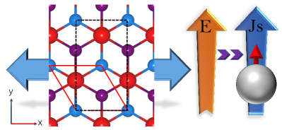
The structure of BiTeI monolayer, without external stress, is presented in Fig. 1. The red solid line represents the unit cell of BiTeI monolayer. It obeys the P3m1 space group and shows the symmetry. For convenience, we take the rectangular cell remarked by black dash line to calculate the effect of uniaxial stress. Through applying the uniaxial tensile stress upon the monolayer along x (or y) direction, the C3v symmetry will be removed and the monolayer keeps the mirror symmetry only, and there appears substantial structural anisotropy between the x and y directions. When a tensile uniaxial stress is along the x (y) axis, there will be a tensile strain along the x (y) axis and a compressive strain along the y (x) axis due to Poisson effect. Actually, we allow the tensile x (y) strain to change actively and determine the compressive y (x) strain by structural optimization, and then we estimate the tensile x (y) stress by where is the total energy of the monolayer under strain along the x (y) direction and is the area of the stretched unit cell. Our study show that the tensile 10% strain along the x or y axis can be achieved by applying 1.71 N/m or 1.82 N/m as the uniaxial stress along the same axis, which indicates that the uniaxial stress on the BiTeI monolayer is experimentally accessible.
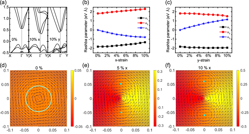
The effect of the uniaxial stress on energy bands of the BiTeI monolayer is shown in Fig. 2 (a), where the left part describes the bands without stress, the middle part those for 10% tensile strain (stress 1.71 N/m) along the x axis, and the right part those for 10% tensile strain (stress 1.82 N/m) along the y axis. When no stress is applied on the monolayer, the conduction bands near the point behave isotropic, and the calculated Rashba parameters (, , and ) are 38.4 meV, 0.042 Å-1, and 1.82 eV Å, in agreement with experimental values Fülöp et al. (2018). When the tensile x-strain reaches 10% (x-stress 1.71 N/m), the conduction band minima along the direction become much lower than those along the direction, which means that the conduction bands near the point become strongly anisotropic. As a result, the calculated Rashba splitting energy and k-vector off-set are equivalent to 27.5 meV and 0.035 Å-1 along the direction, but they become 69.6 meV and 0.060 Å-1 along the direction. When the tensile y-stress 1.82 N/m (10% tensile strain) is applied, the evaluated parameters and are 23.6 meV and 0.031 Å-1 along the direction, but 67.7 meV and 0.060 Å-1 along the direction. These results reveal that the uniaxial x (y) stress makes the lowest conduction bands around the point become two minimum points along the () direction, leading to strong anisotropy in the Rashba parameters.
When the uniaixial stress is applied, the rotational symmetry no longer exists in the stretched BiTeI monolayer, and there remains only mirror symmetry. Under the mirror transformation : , , and . Then we can construct the two-band Hamiltonian for the lowest conduction bands near the point,
| (1) |
where , and the crossing point of the two bands is located at . The three Rashba parameters , , and in the Hamiltonian (1) can be obtained through fitting the conduction bands of strained monolayer, and the strain dependences of the parameters for the x/y stress are shown in Fig. 2 (b,c). It is interesting that is negative for the uniaxial x-stress, but becomes positive for the uniaxial y stress. We can see that the uniaxial stress allows the emergence of new term in the Hamiltonian. It is a new physical phenomenon arising from structural symmetry . Considering the Rashba Hamiltonian with rotational group, there is no term up to the third order of when the symmetry obeys the , , and Vajna et al. (2012). When the point symmetry is or , there is no term in the first order of , but some terms in the third order of are allowed, for example, term Vajna et al. (2012); Fu (2009). Thus we can conclude that uniaxial stress removes the symmetry and thus leads to the emergence of the term, which can cause the inversion of out-of-plane spin polarization.
The eigenvalues of the two-band Hamiltonian (1) can be written as
| (2) |
where refers to the two bands. It should be noted that means . We can obtain the spin expectation values at the momentum near the point,
| (3) | |||
| (4) | |||
| (5) |
The expression (5) means that there emerges a spin z component, in addition to the in-plane components. It is also indicated that the spin y-component and z-component along the line are zero, which is in agreement with our effective Hamiltonian. This phenomenon can be regarded as the result of mirror symmetry. Our first-principles investigation about the spin texture of the lowest conduction band with 10% strain along both x and y axes shows that the out-of-plane spin component has important effect.
Furthermore, we present both the spin textures and energy contours of the lower Rashba band () near the point for 0, 5%, and 10% x-strain in Fig. 2 (d-f). When the Fermi level is shifted downward from the crossing point, the Fermi lines will finally become two separated closed curves, even reduce to two points at the conduction band edge. The change of the Fermi line topology makes a Lifshitz transition. For low electron concentration, there are two Fermi pockets near the conduction band edge, as shown in Fig. 2 (e,f).
III.2 Carrier charge and spin currents through electric field
Now we address electric-field-induced transport phenomena in the stretched BiTeI monolayer in the presence of electron carriers, which can be achieved by charge transferring between van der Waals layers, electric gating, or chemical doping. We suppose that the in-plane electric field is so weak and the electron concentration is so small that there are little changes in the crystal structure and lower conduction bands of the BiTeI monolayer. By keeping in the regime of low electron concentration, we fix the Fermi level near the conduction band edge, as shown in Fig. 3, and the occupied electrons are located in the lower Rashba band in the neighborhood of the points. When a small in-plane electric field is applied, the relaxation time approximation for the Boltzmann equation of the distribution function can be expressed as , where is electron relaxation time and here Hall effect is not taken into consideration Yu et al. (2014); Hamamoto et al. (2017). As the response to the external electric field, the distribution function can be expanded as , where is the distribution function of the system in the absence of , and comes from the iterative substitution of the Boltzmann equation Sodemann and Fu (2015); Morimoto et al. (2016); Yu et al. (2014); Hamamoto et al. (2017).
Consequently, the charge current can be written as Yu et al. (2014); Hamamoto et al. (2017)
| (6) |
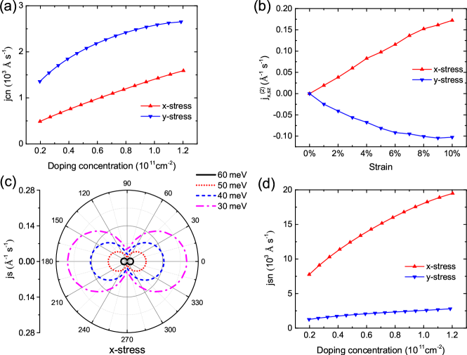
where . We can define a normalized charge current as the ratio of current magnitude to doping electron concentration to describe the current-production efficiency. When the electric field is applied along the x direction, the normalized charge current as the function of electron concentrations under 10% strain along x/y direction are shown in Fig. 3 (a). We can explain this phenomenon with the Drude model where being the concentration of doped electrons. When Fermi level is shifted upward from the band edge, will be increasing, which reduces the value in the system. Thus the normalized current in will be monotonically increasing at this circumstance.
As for the spin current, we take the conventional definition of spin-current operator as , which refers to the spin component flowing along the direction Hamamoto et al. (2017); Rashba (2003); Sinova et al. (2004). It should be especially noted that this definition of spin-current operator will be invalid when the third-power k terms are included in the Hamiltonian Drouhin et al. (2011). The k terms in our Hamiltonian are only to the first order in the presence of small electron concentration ().
Then we obtain the three non-zero components of the spin current near the point,
| (7) | ||||
| (8) | ||||
| (9) |
For the isotropic Rashba model, we have , , and , and then derive , which is the same as Rashba’s result Rashba (2003). The non-zero spin-current expectation will not lead to transport and accumulation of spin under the condition of thermodynamic equilibrium, and it can be connected to a non-Abelian SU(2) field generated by the spin-orbit coupling Tokatly (2008). It can have real spin transport when the Rashba medium is constructed with a spatially modulated spin-orbit parameter Sonin (2007); Sun et al. (2008). For this reason, the zero-order spin current will be addressed no more in the following.
It has been shown that odd (even) orders of the spin (charge) current become zero in the presence of the time-reversal symmetry, and the broken inversion symmetry ensures the existence of non-zero even spin current Hamamoto et al. (2017). So the second-order spin current in our system can occur responding to the electric field. The second-order spin current is defined by Hamamoto et al. (2017)
| (10) | ||||
| (11) |
When the electric field is applied along the x or y direction, there are only three non-zero components for the spin currents, , and . Returning to the isotropic Rashba system, our numerical calculations give that and , which is in agreement with spin current results of isotropic Rashba model Hamamoto et al. (2017). In Fig. 3 (b), we present the spin current under uniaxial stress (010%) along x/y direction when the Fermi level is 10 meV lower than crossing point. When the x-strain (y-strain) reached 10%, the magnitude of is equivalent to . It is clear that the uniaxial stress leads to remarkable spin current , in contrast to the isotropic case.
It is necessary to clarify the real-space texture of the electrically-generated spin current. The magnitude of the spin current along direction ( means the x direction) is given by
| (12) |
When the Fermi level is lower than the crossing point by 60 meV, 50 meV, 40 meV, or 30 meV, our numerical results of the spin currents as functions of are shown in Fig. 3 (c). The spin currents show giant anisotropy in the real space. They increase due to enlarged electron concentration when the Fermi level moves upwards from the conduction and edge. To show the concentration dependence of the maximal spin currents per electron, , we present in Fig. 3 (d) the normalized maximal spin currents as functions of electron concentration for the two cases of the 10% strain along the x and y directions. Here the definition of normalized maximal spin currents is similar to that of normalized charge current. Fig. 3 (d) indicates that the different orientations of uniaxial stress, even under the same electric field (along the x direction), will lead to very different normalized maximal spin currents.
The lifetime in the BiTeI bulk measured by experiment is 3.910-14 s Martin et al. (2013) and then the relation time in the monolayer is assumed as this value. Assuming that the Fermi level is 60 meV lower than the crossing point and the electric field is 1 V m-1 along the x direction, the ratio of the spin current to the charge current is equivalent to 0.09, and the spin current is 1.28109 Å-1s-1 for the x-strain 10%.
III.3 Further discussion for realization
It is useful to show the relationship between the Fermi lvel and the electron concentration. In Table 1 we present the corresponding electron concentrations for the two 10% strains when the Fermi level is lower than the crossing point by 30 meV, 40 meV, 50 meV, and 60 meV. Because doped carrier concentration 1013 cm-2 have been achieved by back-gate gating in transition metal dichalcogenide monolayers Mak et al. (2013); Zhang et al. (2014) and 1014 cm-2 by ion liquid gating in graphene Efetov and Kim (2010); Ye et al. (2011), the electron concentrations ranging from 0.20 to 1.20 cm-2 should be experimentally accessible.
| -30 meV | -40 meV | -50 meV | -60 meV | |
|---|---|---|---|---|
| 10% x-strain | 1.20 | 0.86 | 0.56 | 0.27 |
| 10% y-strain | 1.02 | 0.73 | 0.46 | 0.20 |
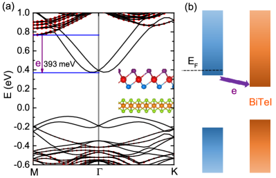
For such 2D materials as the BiTeI monolayer, the electron doping can be achieved by inter-layer charge transferring through van der Waals heterostructure formed with appropriate 2D semiconductors. PtSe2 monolayer is good because it has been synthesised by molten-salt-assisted chemical vapour deposition in the experiment Zhou et al. (2018). We can choose the 33 supercell of BiTeI monolayer and 22 supercell of PtSe2 monolayer to model the heterostructure. The lattice mismatch of the BiTeI/PtSe2 heterostructure is 3%. The side view of the heterostructure and the calculated energy bands are shown in Fig. 4. The conduction band edge of the PtSe2 monolayer is higher than that of the BiTeI monolayer, and the chemically-doped electrons in the PtSe2 monolayer can easily transfer to the BiTeI monolayer. In such ways, the BiTeI monolayer can be doped with electrons, without changing its structure and energy bands.
IV Conclusion
In summary, we use uniaxial stress to manipulate the BiTeI monolayer semiconductor through first-principles calculations and theoretical analyses. Because the uniaxial stress destroys the symmetry, the monolayer has only mirror symmetry, which allows emergence of term in the effective model. We obtain effective anisotropic Rashba Hamiltonian through fitting the Rashba bands with the lowest conduction bands near the point up to the stress of 1.71 N/m for the x axis or 1.82 N/m for the y axis. We find the out-of-plane spin component in the stretched BiTeI monolayer, in addition to usual in-plane spin components in isotropic Rashba model. When electron carriers of low concentration are introduced into the monolayer, an in-plane electric field can induce the first-order charge current and second-order spin currents including a spin current increasing with the uniaxial stress. Such electron carriers can be realized through electron transferring from n-type doped monolayer to the BiTeI monolayer in appropriate van der Waals heterostructures, electric gating, or chemical doping. These make us believe that uniaxial stress and electric field together can open the door for controllable spintronic applications on the basis of good experimentally-realizable 2D materials such as the BiTeI monolayer.
Acknowledgements.
This work is supported by the Nature Science Foundation of China (No.11574366), by the Strategic Priority Research Program of the Chinese Academy of Sciences (Grant No.XDB07000000), and by the Department of Science and Technology of China (Grant No.2016YFA0300701). The calculations were performed in the supercomputer system at Institute of Physics and the Milky Way #2 supercomputer system at the National Supercomputer Center of Guangzhou, Guangzhou, China.References
- Rashba and Sheka (1959) E. I. Rashba and V. I. Sheka, Fiz. Tverd. Tela.: Collected Papers 2, 162 (1959).
- Rashba (1960) E. I. Rashba, Fiz. Tverd. Tela. 2, 1224 (1960).
- Dyakonov (ed.) M. I. Dyakonov (ed.), Spin Physics in Semiconductors, Springer Series in Solid-State Sciences, Vol. 157 (Springer International Publishing AG, 2017).
- Bychkov and Rashba (1984) Y. A. Bychkov and É. I. Rashba, JETP Lett. 39, 78 (1984).
- Manchon et al. (2015) A. Manchon, H. C. Koo, J. Nitta, S. M. Frolov, and R. A. Duine, Nat. Mater. 14, 871 (2015).
- Hu et al. (2018) T. Hu, F. Jia, G. Zhao, J. Wu, A. Stroppa, and W. Ren, Phys. Rev. B 97, 235404 (2018).
- Singh and Romero (2017) S. Singh and A. H. Romero, Phys. Rev. B 95, 165444 (2017).
- Yuan et al. (2018) J. Yuan, Y. Cai, L. Shen, Y. Xiao, J.-C. Ren, A. Wang, Y. P. Feng, and X. Yan, Nano Energy 52, 163 (2018).
- Lu et al. (2017) A.-Y. Lu, H. Zhu, J. Xiao, C.-P. Chuu, Y. Han, M.-H. Chiu, C.-C. Cheng, C.-W. Yang, K.-H. Wei, Y. Yang, Y. Wang, D. Sokaras, D. Nordlund, P. Yang, D. A. Muller, M.-Y. Chou, X. Zhang, and L.-J. Li, Nature Nanotechnology 12, 744 (2017).
- Hanakata et al. (2017) P. Z. Hanakata, A. S. Rodin, A. Carvalho, H. S. Park, D. K. Campbell, and A. H. Castro Neto, Phys. Rev. B 96, 161401 (2017).
- Hanakata et al. (2018) P. Z. Hanakata, A. S. Rodin, H. S. Park, D. K. Campbell, and A. H. Castro Neto, Phys. Rev. B 97, 235312 (2018).
- Noor-A-Alam et al. (2018) M. Noor-A-Alam, M. Lee, H.-J. Lee, K. Choi, and J. H. Lee, J. Phys. Condens. Mat. 30, 385502 (2018).
- Premasiri et al. (2018) K. Premasiri, S. K. Radha, S. Sucharitakul, U. R. Kumar, R. Sankar, F.-C. Chou, Y.-T. Chen, and X. P. A. Gao, Nano Lett. 18, 4403 (2018).
- Zhang and Schwingenschlögl (2018) Q. Zhang and U. Schwingenschlögl, Phys. Rev. B 97, 155415 (2018).
- Ishizaka et al. (2011) K. Ishizaka, M. S. Bahramy, H. Murakawa, M. Sakano, T. Shimojima, T. Sonobe, K. Koizumi, S. Shin, H. Miyahara, A. Kimura, K. Miyamoto, T. Okuda, H. Namatame, M. Taniguchi, R. Arita, N. Nagaosa, K. Kobayashi, Y. Murakami, R. Kumai, Y. Kaneko, Y. Onose, and Y. Tokura, Nat. Mater. 10, 521 (2011).
- Crepaldi et al. (2012) A. Crepaldi, L. Moreschini, G. Autès, C. Tournier-Colletta, S. Moser, N. Virk, H. Berger, P. Bugnon, Y. J. Chang, K. Kern, A. Bostwick, E. Rotenberg, O. V. Yazyev, and M. Grioni, Phys. Rev. Lett. 109, 096803 (2012).
- Landolt et al. (2012) G. Landolt, S. V. Eremeev, Y. M. Koroteev, B. Slomski, S. Muff, T. Neupert, M. Kobayashi, V. N. Strocov, T. Schmitt, Z. S. Aliev, M. B. Babanly, I. R. Amiraslanov, E. V. Chulkov, J. Osterwalder, and J. H. Dil, Phys. Rev. Lett. 109, 116403 (2012).
- Eremeev et al. (2012) S. V. Eremeev, I. A. Nechaev, Y. M. Koroteev, P. M. Echenique, and E. V. Chulkov, Phys. Rev. Lett. 108, 246802 (2012).
- Sakano et al. (2013) M. Sakano, M. S. Bahramy, A. Katayama, T. Shimojima, H. Murakawa, Y. Kaneko, W. Malaeb, S. Shin, K. Ono, H. Kumigashira, R. Arita, N. Nagaosa, H. Y. Hwang, Y. Tokura, and K. Ishizaka, Phys. Rev. Lett. 110, 107204 (2013).
- Monserrat and Vanderbilt (2017) B. Monserrat and D. Vanderbilt, Phys. Rev. Mater. 1, 054201 (2017).
- Bordács et al. (2013) S. Bordács, J. G. Checkelsky, H. Murakawa, H. Y. Hwang, and Y. Tokura, Phys. Rev. Lett. 111, 166403 (2013).
- Sakano et al. (2012) M. Sakano, J. Miyawaki, A. Chainani, Y. Takata, T. Sonobe, T. Shimojima, M. Oura, S. Shin, M. S. Bahramy, R. Arita, N. Nagaosa, H. Murakawa, Y. Kaneko, Y. Tokura, and K. Ishizaka, Phys. Rev. B 86, 085204 (2012).
- Butler et al. (2014) C. J. Butler, H.-H. Yang, J.-Y. Hong, S.-H. Hsu, R. Sankar, C.-I. Lu, H.-Y. Lu, K.-H. O. Yang, H.-W. Shiu, C.-H. Chen, C.-C. Kaun, G.-J. Shu, F.-C. Chou, and M.-T. Lin, Nat. Commun. 5, 4066 (2014).
- Kohsaka et al. (2015) Y. Kohsaka, M. Kanou, H. Takagi, T. Hanaguri, and T. Sasagawa, Phys. Rev. B 91, 245312 (2015).
- Lee et al. (2011) J. S. Lee, G. A. H. Schober, M. S. Bahramy, H. Murakawa, Y. Onose, R. Arita, N. Nagaosa, and Y. Tokura, Phys. Rev. Lett. 107, 117401 (2011).
- Demkó et al. (2012) L. Demkó, G. A. H. Schober, V. Kocsis, M. S. Bahramy, H. Murakawa, J. S. Lee, I. Kézsmárki, R. Arita, N. Nagaosa, and Y. Tokura, Phys. Rev. Lett. 109, 167401 (2012).
- Bahramy et al. (2012) M. S. Bahramy, B.-J. Yang, R. Arita, and N. Nagaosa, Nat. Commun. 3, 679 (2012).
- Eremeev et al. (2017) S. V. Eremeev, I. A. Nechaev, and E. V. Chulkov, Phys. Rev. B 96, 155309 (2017).
- Facio et al. (2018) J. I. Facio, D. Efremov, K. Koepernik, J.-S. You, I. Sodemann, and J. van den Brink, Phys. Rev. Lett. 121, 246403 (2018).
- Qi et al. (2017) Y. Qi, W. Shi, P. G. Naumov, N. Kumar, R. Sankar, W. Schnelle, C. Shekhar, F.-C. Chou, C. Felser, B. Yan, and S. A. Medvedev, Adv. Mater. 29, 1605965 (2017).
- Ma et al. (2014) Y. Ma, Y. Dai, W. Wei, X. Li, and B. Huang, Phys. Chem. Chem. Phys. 16, 17603 (2014).
- Fülöp et al. (2018) B. Fülöp, Z. Tajkov, J. Pető, P. Kun, J. Koltai, L. Oroszlány, E. Tóvári, H. Murakawa, Y. Tokura, S. Bordács, et al., 2D Mater. 5, 031013 (2018).
- Blöchl (1994) P. E. Blöchl, Phys. Rev. B 50, 17953 (1994).
- Kresse and Hafner (1993) G. Kresse and J. Hafner, Phys. Rev. B 47, 558 (1993).
- Perdew et al. (1996) J. P. Perdew, K. Burke, and M. Ernzerhof, Phys. Rev. Lett. 77, 3865 (1996).
- Monkhorst and Pack (1976) H. J. Monkhorst and J. D. Pack, Phys. Rev. B 13, 5188 (1976).
- Vajna et al. (2012) S. Vajna, E. Simon, A. Szilva, K. Palotas, B. Ujfalussy, and L. Szunyogh, Phys. Rev. B 85, 075404 (2012).
- Fu (2009) L. Fu, Phys. Rev. Lett. 103, 266801 (2009).
- Yu et al. (2014) H. Yu, Y. Wu, G.-B. Liu, X. Xu, and W. Yao, Phys. Rev. Lett. 113, 156603 (2014).
- Hamamoto et al. (2017) K. Hamamoto, M. Ezawa, K. W. Kim, T. Morimoto, and N. Nagaosa, Phys. Rev. B 95, 224430 (2017).
- Sodemann and Fu (2015) I. Sodemann and L. Fu, Phys. Rev. Lett. 115, 216806 (2015).
- Morimoto et al. (2016) T. Morimoto, S. Zhong, J. Orenstein, and J. E. Moore, Phys. Rev. B 94, 245121 (2016).
- Rashba (2003) E. I. Rashba, Phys. Rev. B 68, 241315 (2003).
- Sinova et al. (2004) J. Sinova, D. Culcer, Q. Niu, N. A. Sinitsyn, T. Jungwirth, and A. H. MacDonald, Phys. Rev. Lett. 92, 126603 (2004).
- Drouhin et al. (2011) H.-J. Drouhin, G. Fishman, and J.-E. Wegrowe, Phys. Rev. B 83, 113307 (2011).
- Tokatly (2008) I. V. Tokatly, Phys. Rev. Lett. 101, 106601 (2008).
- Sonin (2007) E. B. Sonin, Phys. Rev. B 76, 033306 (2007).
- Sun et al. (2008) Q.-F. Sun, X. C. Xie, and J. Wang, Phys. Rev. B 77, 035327 (2008).
- Martin et al. (2013) C. Martin, E. D. Mun, H. Berger, V. S. Zapf, and D. B. Tanner, Phys. Rev. B 87, 041104 (2013).
- Mak et al. (2013) K. F. Mak, K. He, C. Lee, G. H. Lee, J. Hone, T. F. Heinz, and J. Shan, Nat. Mater. 12, 207 (2013).
- Zhang et al. (2014) Y. Zhang, T. Oka, R. Suzuki, J. Ye, and Y. Iwasa, Science 344, 725 (2014).
- Efetov and Kim (2010) D. K. Efetov and P. Kim, Phys. Rev. Lett. 105, 256805 (2010).
- Ye et al. (2011) J. Ye, M. F. Craciun, M. Koshino, S. Russo, S. Inoue, H. Yuan, H. Shimotani, A. F. Morpurgo, and Y. Iwasa, Proc. Natl. Acad. Sci. 108, 13002 (2011).
- Zhou et al. (2018) J. Zhou, J. Lin, X. Huang, Y. Zhou, Y. Chen, J. Xia, H. Wang, Y. Xie, H. Yu, J. Lei, D. Wu, F. Liu, Q. Fu, Q. Zeng, C.-H. Hsu, C. Yang, L. Lu, T. Yu, Z. Shen, H. Lin, B. I. Yakobson, Q. Liu, K. Suenaga, G. Liu, and Z. Liu, Nature 556, 355 (2018).