Enabling and Exploiting Partition-Level Parallelism (PALP) in Phase Change Memories
Abstract.
Phase-change memory (PCM) devices have multiple banks to serve memory requests in parallel. Unfortunately, if two requests go to the same bank, they have to be served one after another, leading to lower system performance. We observe that a modern PCM bank is implemented as a collection of partitions that operate mostly independently while sharing a few global peripheral structures, which include the sense amplifiers (to read) and the write drivers (to write). Based on this observation, we propose PALP, a new mechanism that enables partition-level parallelism within each PCM bank, and exploits such parallelism by using the memory controller’s access scheduling decisions. PALP consists of three new contributions. First, we introduce new PCM commands to enable parallelism in a bank’s partitions in order to resolve the read-write bank conflicts, with no changes needed to PCM logic or its interface. Second, we propose simple circuit modifications that introduce a new operating mode for the write drivers, in addition to their default mode of serving write requests. When configured in this new mode, the write drivers can resolve the read-read bank conflicts, working jointly with the sense amplifiers. Finally, we propose a new access scheduling mechanism in PCM that improves performance by prioritizing those requests that exploit partition-level parallelism over other requests, including the long outstanding ones. While doing so, the memory controller also guarantees starvation-freedom and the PCM’s running-average-power-limit (RAPL).
We evaluate PALP with workloads from the MiBench and SPEC CPU2017 Benchmark suites. Our results show that PALP reduces average PCM access latency by , and improves average system performance by compared to the state-of-the-art approaches.
1. Introduction
Modern phase change memory (PCM) devices (Fagot et al., 2018; Lung et al., 2016; Castellani et al., 2016; Navarro et al., 2018; Villa, 2018; Lee et al., 2009) can serve multiple requests in parallel using different PCM banks (Lung et al., 2016). Unfortunately, when two requests go to the same bank, they have to be served serially. This is known as bank conflict. Bank conflicts reduce system performance by lowering the PCM bandwidth utilization, causing CPU cores to stall. To estimate the impact of bank conflicts on performance, we plot the distribution of read-read, read-write, and write-write bank conflicts in 15 8-core workloads for a PCM memory of 8GB capacity and with eight 1GB banks (see our evaluation methodology in Section 5). We make the following two observations.
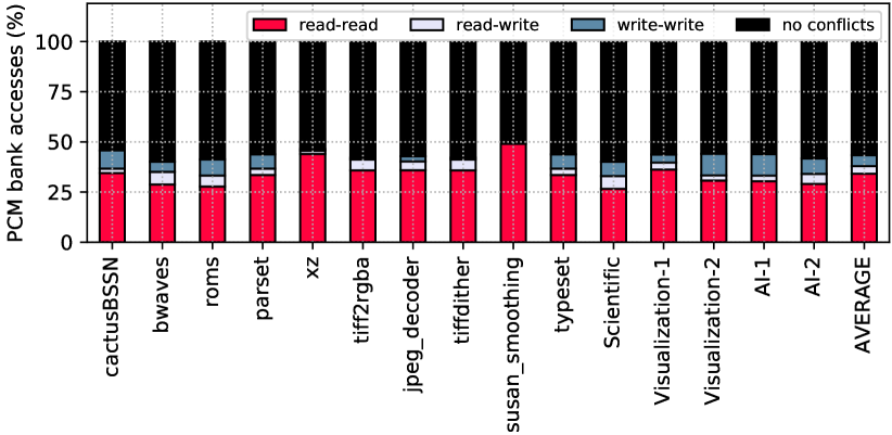
First, on average, 43% of PCM requests in these workloads generate bank conflicts. This is due to the high temporal and spatial access locality in these workloads that lead to repeated accesss to multiple rows that map to the same bank. Second, read-read bank conflicts outnumber read-write and write-write bank conflicts for all workloads, averaging to 34% of all PCM requests (79% of all bank conflicts). The read-write and write-write bank conflicts are fewer than read-read bank conflicts because write requests are fewer to begin with as they go through an extra level of cache implemented as eDRAM. The read requests, on the other hand, go directly to PCM, bypassing the eDRAM cache. We conclude that by resolving both read-read and read-write bank conflicts in PCM, system performance can be improved significantly. We demonstrate average performance improvement in Section 6.1 for our evaluated workloads. As core count increases, bank conflicts also increase and become a bigger performance bottleneck (Hassan et al., 2016; Kim et al., 2012; Hassan et al., 2019).
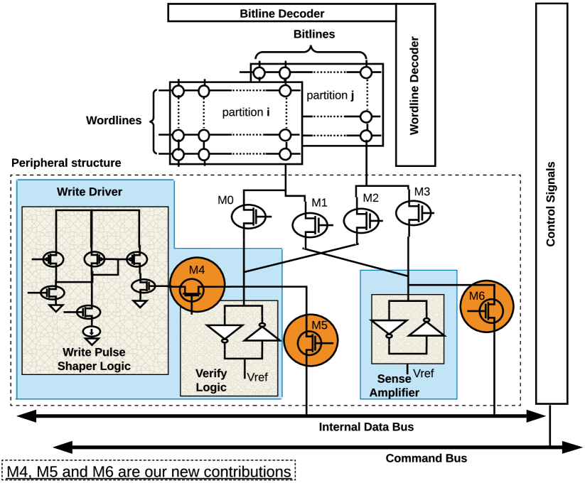
Our goal is to improve performance by resolving bank conflicts in PCM devices. To this end, we analyze the internal architecture of a PCM bank (see Figure 2 for details). We observe that a PCM bank is implemented as a collection of partitions (Lung et al., 2016) that operate mostly independently while sharing a few global peripheral structures, which include the sense amplifiers (to read) and the write drivers (to write). A peripheral structure has high area overhead primarily due to the write driver logic (Cho et al., 2005; Sandhu et al., 2018; Dray and Wei, 2018), which needs to generate high current profiles for the SET (100A) and RESET (300A) programming of the PCM cells. Due to this high area overhead, PCM manufacturers integrate only a small number of these structures per bank to improve PCM density (Villa, 2018). For instance, in the recent PCM prototypes (Lung et al., 2016; Villa, 2018), there are only 128 peripheral structures per bank, which are shared across all 16 partitions in the bank.
Based on our key observation, we propose PALP, a new mechanism that enables partition-level parallelism in a PCM bank, and exploits such parallelism by modifying only the memory controller’s access scheduling decisions. We make the following three novel contributions.
Contribution 1: We propose a new mechanism to enable read-write parallelism in a PCM bank’s partition using the bank’s peripheral structures to resolve the read-write bank conflicts. To this end, we introduce a new PCM command called READ-WITH-WRITE (RWW), and provide its detailed timing requirements.
Contribution 2: We propose simple circuit modifications to introduce a new operating mode for the write drivers, with which they can also serve read requests. When configured in this new mode, the write drivers can resolve the read-read bank conflicts, working jointly with the sense amplifiers. To this end, we introduce a new PCM command called READ-WITH-READ (RWR), and provide its detailed timing requirements.
Contribution 3: We propose a new memory access scheduling mechanism that prioritizes those PCM requests that exploit a PCM bank’s partition-level parallelism, over other requests, including the long outstanding ones. This straightforward and greedy performance-oriented policy is controlled in two ways. First, the memory controller ensures that no request is starved, i.e., backlogged excessively, forcefully serving the outstanding request otherwise, to guarantee starvation-freedom (Kim et al., 2010). Second, the memory controller ensures that the power consumption of the active partitions within the bank is not too high, forcefully serializing requests to the bank otherwise, to guarantee the running average power limit (RAPL) (David et al., 2010).
We implement PALP for DRAM-PCM hybrid main memory systems (Qureshi et al., 2009; Dhiman et al., 2009; Liu et al., 2018; Li et al., 2017; Zhao et al., 2014; Yoon et al., 2012; Meza et al., 2012; Ham et al., 2013; Bock et al., 2016; Lin et al., 2017; Yu et al., 2017; Meza et al., 2013), which use DRAM as a cache to PCM. Given the still speculative state of the PCM technology, we describe PALP based on the architecture and memory timings of IBM’s PCM prototype (Lung et al., 2016). We evaluate PALP with workloads from the MiBench (Guthaus et al., 2001) and SPEC CPU2017 (Bucek et al., 2018) benchmark suites. Our results show that PALP reduces average PCM access latency by , and improves average system performance by compared to the state-of-the-art approaches. As PALP exploits the PCM bank’s partition-level parallelism using the memory controller’s access scheduling decision, it can be easily combined with orthogonal mechanisms: (1) those aiming to reduce the number of write accesses to PCM (Dhiman et al., 2009; Li et al., 2017; Bock et al., 2016), and (2) those aiming to improve PCM’s cell endurance (Seong et al., 2010; Akram et al., 2018).
Although our work is inspired by the notion of subarray-level parallelism (SALP) in DRAM (Kim et al., 2012), exploiting parallelism within PCM banks is unique in the following two aspects. First, while many subarrays can be active simultaneously in a DRAM, PCM’s peripheral structures allow only two partitions to be active simultaneously in a PCM bank (Barkley et al., 2017). Second, while subarray-level parallelism in DRAM can resolve any bank conflict, partition-level parallelism in PCM can resolve only the read-read or read-write bank conflicts. These unique properties of PALP lead to different performance trade-offs, which we present in Section 6.
The closest state-of-the-art PCM mechanisms, such as (Zhou et al., 2016; Yue and Zhu, 2013b), have only addressed the read-write bank conflicts in PCM, assuming a simple first-come-first-serve (FCFS) scheduling policy (Rixner et al., 2000). We demonstrate in Section 4.3 that the FCFS policy cannot efficiently exploit each PCM bank’s partition-level parallelism. We not only resolve both the read-read and read-write bank conflicts in PCM, but also develop a new performance-oriented scheduling policy to better exploit such partition-level parallelism. Our PALP design is based on IBM’s PCM chip interfaced with ARMv8-A (aarch64) processor using the DDR4 protocol. In Table 1, we summarize the state-of-the-art mechanisms and highlight the contributions of this paper.
| Mechanism | Read-Write | Read-Read | Scheduling | Memory | Memory | Memory |
|---|---|---|---|---|---|---|
| Bank Conflicts | Bank Conflicts | Interface | Technology | Power | ||
| Baseline (Arjomand et al., 2016) | FCFS | DDR2 | PCM | not controlled | ||
| (Zhou et al., 2016; Yue and Zhu, 2013b) | FCFS | not considered | PCM | not controlled | ||
| SALP (Kim et al., 2012) | FR-FCFS | DDRx | DRAM | not controlled | ||
| PALP | new | DDRx | PCM | RAPL |
2. Background on PCM
This section provides a brief background on PCM organization and operation required to understand PALP. PCM, like DRAM, is organized hierarchically (Lung et al., 2016). An example PCM memory of capacity has channels, with 4 ranks per channel, and 8 banks per rank. A PCM bank has partitions, each of which is an arrays of wordlines and bitlines. A PCM bank has peripheral structures, which include the sense amplifiers (to read) and the write drivers (to write). The peripheral structures in PCM banks allow to read and program 128 PCM cells in parallel. Therefore, the read and write granularity is bits (the size of a memory line).
A PCM cell is built with the chalcogenide alloy (e.g., Ge2Sb2Te5 (Ovshinsky, 1968)), and is connected to a bitline and a wordline using an access device. The amorphous phase (RESET) in this alloy has higher resistance than the crystalline phase (SET). To RESET a PCM cell, a high current pulse of short duration is applied and quickly terminated. To SET a PCM cell, the chalcogenide alloy is heated above its crystallization temperature, but below its melting point for a long duration. Finally, to read the content of a PCM cell, a small electrical pulse is applied without inducing any phase change in the material. To serve a memory request that accesses data at a particular row and column address within a partition, a memory controller issues three commands to a PCM bank.
-
•
ACTIVATE(A): activate the wordline and enable the access device for the PCM cells to be accessed.
-
•
READ(R)/WRITE(W): drive read or write current through the PCM cell. After this command executes, the data stored in the PCM cell is available at the output terminal of the sense amplifier, or the write data is programmed to the PCM cell.
-
•
PRECHARGE(P): deactivate the wordline and bitline, and prepare the bank for the next access.
The A-A interval (tRC) for the same bank is cycles for a write request, and cycles for a read request; A-W/R (tRCD) is 1 cycle; the read latency (RL) is 10 cycles; the write latency (WL) is 3 cycles; and the write recovery time (tWR) is 35 cycles. These timing parameters are based on a 266MHz memory clock and a DDR2 interface (Lung et al., 2016) (see also Table 5 for our simulation parameters).
3. Enabling Partition-Level Parallelism in PCM
Figure 2 illustrates a PCM bank’s peripheral structures in detail (Fagot et al., 2018; Lung et al., 2016; Navarro et al., 2018; Villa, 2018; Villa et al., 2010; Goda et al., 2018). There are 128 peripheral structures, which are shared across all bitlines in the bank. Each peripheral structure is connected to all the partitions in the bank. To simplify our discussion, we illustrate only one peripheral structure, which is connected to the two partitions and . The peripheral structure contains the sense amplifier (to read) and the write driver (to write), which are connected to the two partitions using the NMOS transistors M0, M1, M2, and M3. These transistors are turned ON or OFF, based on the partition that needs to be accessed. The bitline and wordline decoders are used to connect the PCM cell at a particular row and column address to the peripheral structure.
3.1. Resolving read-write bank conflicts in PCM
Table 2 reports how the transistors M0, M1, M2, and M3 are configured to serve read and write requests. Observe that only one transistor is ON in the baseline PCM design (e.g., (Arjomand et al., 2016)) to serve a read or write request from the bank.
| Operation | M0 | M1 | M2 | M3 |
|---|---|---|---|---|
| write to partition i | ON | OFF | OFF | OFF |
| read from partition i | OFF | ON | OFF | OFF |
| write to partition j | OFF | OFF | ON | OFF |
| read from partition j | OFF | OFF | OFF | ON |
To investigate what is actually needed to resolve the read-write bank conflicts in PCM, we take a closer look at the connections of M0, M1, M2, and M3. Observe that if transistors M0 and M3 (or M1 and M2) are simultaneously enabled, the sense amplifier can read a PCM cell from partition , while the write driver is programming a PCM cell in partition (or vice versa). Table 3 summarizes our findings. Some transistor configurations can lead to data corruption. For example, if M0 = OFF, M1 = ON, M2 = OFF, M3 = ON, (the last entry in the table), then the data from two different partitions (i.e., two different PCM cells) will be connected to the sense amplifier. This compromises the integrity of the data to be read at the output of the sense amplifier. We mark all such table entries as invalid.
| Operation | M0 | M1 | M2 | M3 |
|---|---|---|---|---|
| write to partition i, read from partition j | ON | OFF | OFF | ON |
| read from partition i, write to partition j | OFF | ON | ON | OFF |
| invalid | ON | ON | OFF | OFF |
| invalid | OFF | OFF | ON | ON |
| invalid | ON | OFF | ON | OFF |
| invalid | OFF | ON | OFF | ON |
This is precisely the parallelism we seek in PCM banks, which can resolve read-write bank conflicts, only when the two conflicting requests are to two different partitions within the bank. To this end, we propose the following two architectural enhancements.
-
•
First, the memory controller must issue two back-to-back ACTIVATE commands to the PCM bank to decode the wordline and bitline addresses in the two partitions.
-
•
Second, the memory controller must configure the transistors to connect the two partitions, one to the write drivers, and the other to the sense amplifiers.
To accomplish these actions, we introduce a new PCM command:
-
•
READ-WITH-WRITE (RWW): connect the PCM bank’s sense amplifiers and write drivers to the two decoded partitions.
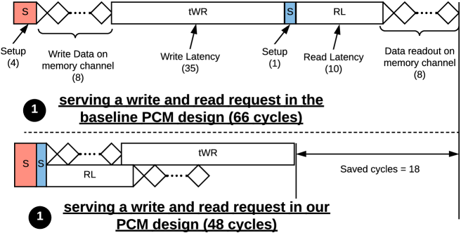
Figure 3 compares how a write and read request is scheduled in baseline PCM ( ❶ ) with our proposed PCM ( ❷ ) in which the memory controller exploits the PCM bank’s partition-level parallelism. Following are the respective command sequences.
Baseline PCM:
-
•
ACTIVATE address in
-
•
WRITE
-
•
PRECHARGE
-
•
ACTIVATE address in
-
•
READ
-
•
PRECHARGE
-
–
Service time = 47 + 19
-
= 66 cycles
Proposed PCM:
-
•
ACTIVATE address in
-
•
ACTIVATE address in
-
•
READ-WITH-WRITE
-
•
PRECHARGE
-
–
Service time = 1 + 47
-
= 48 cycles
❶
❷
In the baseline PCM design, A-W-P takes 47 cycles and A-R-P takes 19 cycles (see Figure 3), contributing to a total of 66 cycles to serve these two requests. In our PCM design, A-RWW-P takes 47 cycles, during which the write recovery time (tWR) partially overlaps with the read latency (RL). The extra 1 cycle is due to the second ACTIVATE command. The total service latency is 48 cycles for serving a read and write request mostly in parallel, a reduction of 18 cycles (27%) over the baseline.
3.2. Resolving read-read bank conflicts in PCM
From the write driver’s internal circuit diagram shown in Figure 2, we observe that the write driver can be viewed as a collection of two components – the write pulse shaper logic, which generates the current pulses necessary for the PCM cell’s SET and RESET operations, and the verify logic, which verifies the correctness of these operations. These two circuit components together serve write requests from the bank using a PCM write scheme known as program-and-verify (P&V) (Nirschl et al., 2007; Goda et al., 2018). The verify logic essentially consists of two cross-coupled inverters, which can be configured as a sense amplifier, similar to the one that is already part of the peripheral circuit. Based on this observation, we propose simple circuit modifications to introduce the decoupling transistor M4 (see Fig. 2), which can be configured when needed, to decouple the verify logic from the write pulse shaper logic. As a result of this modification, we introduce two operating modes for the write driver. In the decoupled mode, the verify logic can serve read requests concurrently with those served by the sense amplifiers. In the write mode, the verify logic, together with the write pulse shaper logic, can serve P&V-based write operations. Table 4 summarizes our findings.
| Operating | Write driver circuit | Sense Amplifier | Operations | |
|---|---|---|---|---|
| Modes | Pulse shaper logic | Verify logic | Enabled | |
| write | one write request | |||
| decoupled | two read requests | |||
This is precisely the read-read parallelism we seek in a PCM bank to resolve a read-read bank conflict, where the two conflicting requests are to two different partitions within the bank. To enable this parallelism, we introduce two new PCM commands:
-
•
DECOUPLE (D): set M4 = OFF.
-
•
READ-WITH-READ (RWR): connect the sense amplifiers and verify logic of the write drivers to the two decoded partitions.
To facilitate arbitration of the data bus for transferring two sets of read data back to the memory controller, we introduce two more transistors M5 and M6. In the write mode, M5 = OFF and M6 = ON. In the decoupled mode, the memory controller first retrieves the sense amplifiers’ data in 8 cycles. It then sets M5 = ON and M6 = OFF in the next cycle, which enables the verify logic’s data to be retrieved in the following 8 cycles. The data transfer latency from PCM to the memory controller is therefore cycles. For this purpose, we introduce our final new PCM command:
-
•
TRANSFER (T): sets M5 = ON and M6 = OFF.
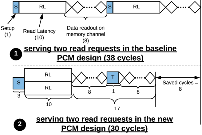
Figure 4 compares how two read requests are scheduled in the baseline PCM design ( ❶ ) with our PCM design ( ❷ ), where the memory controller exploits the PCM bank’s partition-level parallelism. Following are the respective command sequences.
Baseline PCM:
-
•
ACTIVATE address in
-
•
READ
-
•
PRECHARGE
-
•
ACTIVATE address in
-
•
READ
-
•
PRECHARGE
-
–
Service time = 19 + 19
-
= 38 cycles
Proposed PCM:
-
•
ACTIVATE address in
-
•
ACTIVATE address in
-
•
DECOUPLE
-
•
READ-WITH-READ
-
•
TRANSFER
-
•
PRECHARGE
-
–
Service time = 1 + 1 + 1 + 10 +
-
8 + 1 + 8 = 30 cycles
❶
❷
In the baseline PCM design, each takes 19 cycles. The total service latency is therefore, 38 cycles to serve two read requests serially from partitions and . In our PCM design, the memory controller issues the following commands: . In our new design, RWR takes 10 cycles, during which the read latency (RL) of the two read requests are overlapped. The total service latency is therefore cycles, considering 8+1+8 = 17 cycles for the data transfer from PCM to the memory controller as shown in Figure 4 ( ❷ ).
4. Exploiting Partition-Level Parallelism in PCM
This section describes our new memory access scheduling policy to exploit each PCM bank’s partition-level parallelism, which we describe how to enable in Section 3.
4.1. High-level overview
The key idea of our scheduling policy is to maximize partition-level parallelism as long as the running average power limit (RAPL) is not violated and a request does not become delayed too much.
At a high level, the memory controller maintains a read-write queue (rwQ) to store PCM requests. We implement rwQ as a FIFO. After scheduling a request from the rwQ, the memory controller checks to see if there is any outstanding request that can be scheduled exploiting the PCM bank’s partition-level parallelism. If so, the request is scheduled along with the ongoing request, and the memory timing parameters are set accordingly. Otherwise, the memory controller selects the oldest request in the rwQ to be scheduled after completing the ongoing one.
Figure 5 summarizes the flowchart of our new memory access scheduling policy.
4.2. Detailed design
To explain our new memory access scheduling policy, we introduce the following notation
| : starvation threshold | |||
| : number of memory clock cycles for which | |||
| : power consumption of all sense amplifiers in a bank | |||
| : power consumption of all write drivers in a bank | |||
| : total number of memory clock cycles elapsed | |||
| : running average power consumption | |||
| : running average power limit (David et al., 2010) for the PCM device |
We estimate the power consumed to resolve a read-read (R-R) and read-write (R-W) bank conflict as follows:
| (1) |
The timing parameters are as follows: 30 cycles for resolving the read-read (R-R) conflict, and 48 cycles for the read-write (R-W) conflict (see also Table 5).
The pseudo-code of our new memory access scheduling policy is shown in Algorithm 1.
4.3. Significance of PALP’s scheduling policy
We provide some intuition, via an example, as to why (1) enabling each PCM bank’s partition-level parallelism is not sufficient to significantly improve performance, unless there is a scheduling policy that explicitly exploits such parallelism, and (2) why PALP’s scheduling policy outperforms the standard FCFS policy (Rixner et al., 2000), which is commonly used by many PCM memory controllers.
Figure 6 illustrates an example showing how the memory controller schedules six PCM requests to the same bank. In ( ❶ ) we illustrate the FCFS policy of the Baseline (Arjomand et al., 2016), where no more than one partition is active at any time. Using the timing parameters listed at the bottom of this figure, the total PCM service latency is 170 cycles.
❶
❷
❸
In ( ❷ ) we illustrate the FCFS policy with partition-level parallelism in PCM banks. The PCM request is scheduled with by issuing the new PCM command RWW using partitions 1 and 3. This resolves the read-write bank conflict. The PCM request is scheduled with by issuing the new PCM command RWR using partitions 4 and 3. This resolves the read-read bank conflict. We note that requests and are both to partition 1, and therefore scheduled serially. In this example, more than one partition can be active, which enables the total PCM service latency to go down to 144 cycles, a reduction of 15.3% over the baseline.
Finally, in ( ❸ ) we illustrate one example schedule obtained using PALP’s new memory access scheduling policy. The memory controller re-orders PCM requests in the read-write queue to maximize partition-level parallelism. We observe 1) request is scheduled with , and request is scheduled with by issuing two RWW PCM commands and 2) request is scheduled with by issuing a RWR PCM command. This reduces the total PCM service latency to 126 cycles, a further savings of 12.5% compared to ❸ .
Overall, PALP improves performance by 25.8% over the baseline ❷ in this example. In Section 6, we report PALP’s application-level performance improvement for all our evaluated workloads.
5. Evaluation Methodology
To evaluate PALP, we develop a full-system simulator with the following components.
- •
-
•
We use a hybrid DRAM-PCM memory system. DRAMPower (Chandrasekar et al., 2012) is used to estimate its power consumption.
-
•
In-house cycle-level PCM simulator for 8GB, 16GB, and 32GB PCM with DDR4 interface. This is based on Ramulator (Kim et al., 2016), a cycle-accurate main memory simulator. Power and latency parameters are based on IBM’s 20nm PCM (Lung et al., 2016), with DDR4 interface parameters (Association et al., 2012). Our simulator is available for download at (Song et al., 2019).
Table 5 shows our simulation parameters.
| Processor | 8 cores, 3 GHz, out-of-order |
|---|---|
| L1-I/D cache | Private 64KB per core, 4-way |
| L2 cache | Private 512KB per core, 8-way |
| L3 cache | Shared 4MB, 16-way |
| eDRAM cache | Shared, writes-only, and on-chip |
| 4MB (default), 8MB, 16MB, 32MB, and 64MB eDRAMs are evaluated | |
| Main memory | 8GB (default), 16GB, and 32GB PCMs are evaluated |
| (4 channels, 4 ranks/channel, 8 banks/rank.) | |
| Memory interface = DDR4 | |
| Memory clock = 256MHz | |
| A-R-P / A-W-P = 19 cycles / 47 cycles | |
| tWR / RL = 35 cycles / 10 cycles | |
| A-RWW-P / A-RWR-P = 48 cycles / 30 cycles |
5.1. Evaluated techniques
We evaluate the following techniques:
-
•
Baseline: The Baseline technique (Arjomand et al., 2016) maximizes PCM performance by serving multiple requests in parallel across all banks. It uses the FCFS policy and does not exploit partition-level parallelism.
-
•
MultiPartition: The MultiPartition technique (Zhou et al., 2016) can resolve the read-write bank conflicts in PCM by exploiting the presence of partitions in a bank. The original design of (Zhou et al., 2016) uses the FCFS policy, which provides very small benefit over the Baseline (according to our evaluations). For a fair comparison with PALP, we implemented out-of-order scheduling for this technique. This scheduling policy explicitly prioritizes requests that exploit read-write parallelism in PCM. Although (Zhou et al., 2016) does not consider memory interface timings, we implement the MultiPartition technique with the DDR4 interface to fairly and accurately estimate its performance.
-
•
PALP: Our mechanism enables each PCM bank’s partition-level parallelism, and uses our new memory access scheduling policy to optimize performance by prioritizing requests that can exploit such partition-level parallelism. PALP can resolve both read-write and read-read bank conflicts.
The address mapping for all our evaluated systems is based on Micron’s DDR4 Datasheet (Micron, 2014). We show an example of how a memory address is mapped in PCM with 4 channels, 4 ranks/channel, 8 banks/rank, 8 partitions/bank: [36:35]=rank, [34:23]=row, [22:14]=column, [13: 11]=partition, [10:8]=bank, [7:6]=channel, [5:0]=byte within a cache line. We also evaluated various different forms of address interleaving, ranging from cache block interleaving to row interleaving (Kim et al., 2010). Even though exact numerical benefits differ, our mechanism works and improves performance for all evaluated address mappings.
5.2. Evaluated workloads
Table 6 reports the evaluated workloads. These workloads were chosen because they have at least 1 memory access per 1000 instructions out of the 64MB on-chip eDRAM cache. Although SPEC CPU2017 workloads are commonly used for evaluating high performance systems, recent works suggest that these workloads are also representative of many emerging applications that are regularly enabled by users on their mobile phones (Panda et al., 2018).
| MiBench workloads (Guthaus et al., 2001) | |
| tiff2rgba, jpeg_decode, tiffdither, susan_smoothing, typeset | |
| SPEC CPU2017 workloads (Bucek et al., 2018) | |
| cactusBSSN, bwaves, roms, parset, xz | |
| Mixed (parallel) applications | |
| AI-1 (4 copies each of deepsjeng, leela), AI-2 (4 copies each of mcf, exchange2), Visualization-1 (4 copies each of povray, blender), Visualization-2 (4 copies each of povray, imagick), Scientific (4 copies each of cactusBSSN, bwaves) | |
5.3. Figures of Merit
We report the following figures of merit in this work to evaluate different mechanisms:
-
1.
Execution Time: The time it takes to finish a workload.
-
2.
Queuing Delay: The total number of memory cycles spent by a request in the rwQ, averaged over all PCM requests. The delay of each request is measured as the time difference between when a request is inserted in the queue and the time when it is scheduled to PCM.
-
3.
Access Latency: The sum of queuing delay and the PCM service latency, averaged over all PCM requests.
-
4.
PCM Power Consumption: The total power consumed for activating partitions and peripheral structures within PCM banks.
6. Results and Discussion
6.1. Overall system performance
Figure 7 reports the execution time of each of our workloads for each of our evaluated systems normalized to the Baseline system. The simulator is configured for the default settings of 4MB eDRAM cache and a 8GB PCM. We make the following two observations.
First, MultiPartition has higher performance than the Baseline (32% lower average execution time). This improvement is because MultiPartition resolves read-write bank conflicts in PCM. Second, PALP has the highest performance among all the three evaluated systems (PALP has 51% lower average execution time than the Baseline, and lower average execution time than MultiPartition). This performance improvement is because 1) PALP resolves both read-read and read-write bank conflicts, and 2) PALP’s memory access scheduling policy is optimized to maximize both read-read and read-write partition-level parallelism to achieve higher performance.
6.2. Queuing delay
Figure 8 reports the queuing delay of each of our workloads for each of our evaluated systems normalized to the Baseline system. The simulator is configured for the default settings of 4MB eDRAM cache and a 8GB PCM. We make the following two observations.
First, the average queuing delay of MultiPartition is 34% lower than Baseline. This is because MultiPartition reduces the average delay of the outstanding write requests by scheduling them concurrently with read requests that are to different partitions within PCM banks (exploiting read-write parallelism). Second, the average queuing delay of PALP is the lowest (52% lower than the Baseline and 26% lower than MultiPartition). This reduction is because PALP also reduces the queuing delay of read requests by scheduling them concurrently with those that are to different partitions within PCM banks (exploiting read-read parallelism).
6.3. Access latency
Figure 9 reports the access latency of each of our workloads for each of our evaluated techniques normalized to the Baseline, using the default settings of our simulator. We make the following two observations.
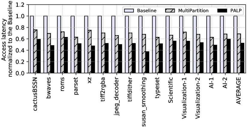
First, the average access latency of MultiPartition is 31% lower than the Baseline. This reduction is a result of performance improvement due to exploiting read-write partition-level parallelism in PCM, as we have discussed in Section 3.1. Second, the average access latency of PALP is the lowest among all the three systems (47% lower than the Baseline, and lower than MultiPartition). This reduction is due to the significant reduction of the PCM service latency achieved by exploiting both read-read and read-write partition-level parallelism in PCM banks.
6.4. PCM power consumption
Figure 10 reports the average and peak power consumption of PALP for each of our workloads. The simulator is configured for the default settings of 4MB eDRAM cache and a 8GB PCM. We also report the RAPL limit, which is 0.4pJ per access. This limit is what is specified in the PCM datasheet (Lung et al., 2016). We make the following two observations.
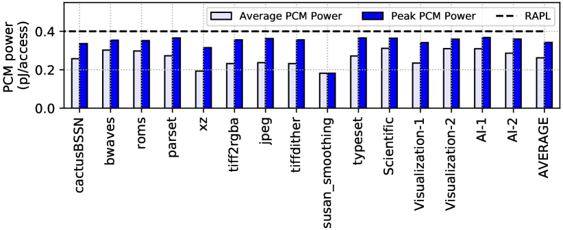
First, both average and peak PCM power consumption of PALP is within the RAPL limit. The average PCM power is at least 0.08pJ/access lower than the RAPL limit, while the peak PCM power is at least 0.03pJ/access lower. Our memory access scheduler explicitly estimates the increase in power consumption when more than one partition is active to exploit partition-level parallelism, and serializes requests to PCM anytime the RAPL limit is estimated to be exceeded. None of the prior works take power consumption into account while exploiting PCM bank’s partition-level parallelism. As a result, the RAPL limit cannot be guaranteed in these works. Second, our technique allows the exploration of performance and power trade-offs. We observe that reducing the RAPL limit to 0.35pJ/access will not hurt performance when our technique is employed. In fact, system designers can potentially use our technique to estimate the RAPL needed to achieve a desired performance target and distribute the surplus power budget to other system components.
6.5. Latency, power, and area overheads
We evaluate the latency and power overhead of PALP against the Baseline PCM design using SPICE simulations (Emam et al., 1997) with 20nm technology files from (Sinha et al., 2012). For the Baseline design, we use IBM’s PCM architecture (Lung et al., 2016). In evaluating our design overheads, we use the industry standard low standby power (LSTP) multi-gate transistors. We also use copper interconnect parasitics (Schuddinck et al., 2012) in our SPICE simulation to model wire delays. Finally, we modeled process variation using the guidelines presented in (Xiong and Bokor, 2003). In Table 7, we report the latency and power overheads of PALP.
| Design | Technology | Vdd | Critical Path Delay | Power |
|---|---|---|---|---|
| Type | (V) | (ps) | (pJ/access) | |
| Baseline (Lung et al., 2016) | Double-gate | 0.9 | 1159.2 | 0.311 |
| Proposed PALP | Double-gate | 0.9 | 1453.2 | 0.364 |
We observe that due to the new circuits that we introduce, the critical path delay has increased by 25.3%. However, the clock cycle time is 3.9ns for 256MHz rated memory clock, which is much higher than the critical path delay of 1453.2ps. We believe that the introduced logic is unlikely to create setup or hold violations at this rated clock frequency.
Our design also increases the power consumption by 17% over the Baseline design of a single peripheral structure consisting of a sense amplifier and our new write driver.
Finally, we observe that PALP has an area overhead of 1.15% compared to the area of each peripheral structure. This overhead is negligible compared to the area of a 1GB PCM bank, which is mm2 at nm technology node.
6.6. Effect of PALP with different PCM capacities
Figure 11 reports the execution time of each of our workloads with PALP using PCM capacities of 16GB and 32GB, normalized to the default configuration using PALP with 8GB PCM. The eDRAM capacity is configured to 4MB for all these configurations. We make the following two observations from our study.
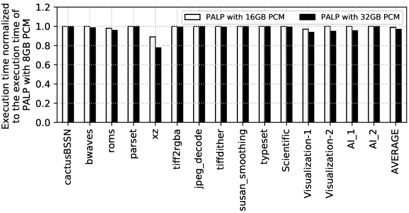
First, for most workloads, we observe a very little performance improvement when the PCM capacity is increased from 8GB to 32GB. This is because these workloads have small working sets, for which a 8GB PCM is sufficient. Second, for xz we observe a significant performance improvement when we increase the PCM capacity to 16GB and 32GB due to xz’s large working set. For this workload, the higher the number of PCM banks, the better the performance of PALP. This is because PALP can exploit more parallelism in more partitions in PCM that exist in more banks.
6.7. Effect of different eDRAM capacities
Figure 12 reports the execution time of each of our workloads with PALP, normalized to the default configuration using PALP with 4MB eDRAM cache. We report results for PALP with eDRAM capacity of 8MB, 16MB, and 32MB. The PCM capacity is configured to 8GB. We make the following two observations.
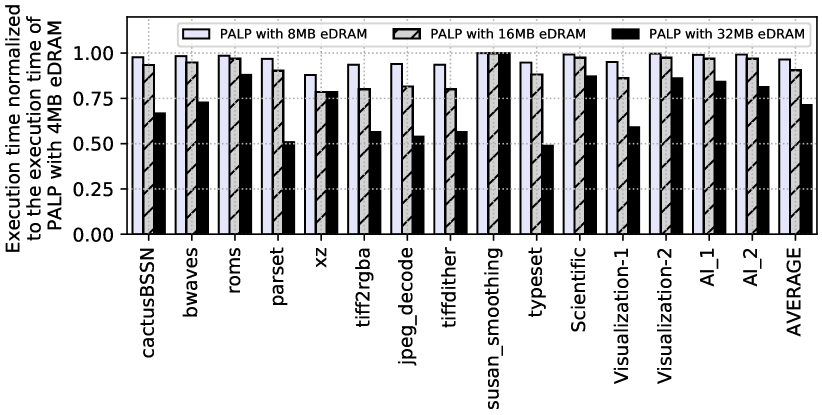
First, for most workloads, as we increase the capacity of the eDRAM cache we observe a significant improvement in performance (lower execution time). This is because with a larger eDRAM cache capacity, more write requests are absorbed in the eDRAM, leaving only the read requests to be queued in the rwQ. This impacts the execution time in the following two ways: 1) the latency to service long write requests is reduced, and 2) the memory controller now has more flexibility to exploit read-read parallelism from the outstanding read requests. Second, for susan_smoothing, we observe a marginal change in performance when we increase the eDRAM capacity to 32MB. This is because there are only a small number of write requests in this workload to begin with, and therefore the workload’s performance is insensitive to the size of the eDRAM cache, which buffers only write requests.
6.8. Effect of different interface timings
Figure 13 reports the execution time of each of our workloads for PALP with DDR2 and DDR4 interfaces, normalized to the Baseline using the default settings of our simulator. We make the following two observations.
First, the performance of PALP with DDR2 and DDR4 interfaces are both better than the Baseline. The average execution time of PALP with the DDR2 interface is 33% lower than the Baseline, while that with the DDR4 interface is 51% lower than the Baseline. Second, we observe that the execution time of PALP decreases when the memory interface is changed from DDR2 to DDR4. The average performance improves by 27% when DDR4 interface is used. This increase is because the data transfer rate is doubled in DDR4 compared to DDR2. A complete exploration of all DRAM standards is a vast undertaking, and is beyond the scope of this work (see, for instance, (Ghose et al., 2019)). We conclude that PALP improves performance for multiple DDRx interface standards.
6.9. Effect of different design thresholds
6.9.1. RAPL limit:
Figure 14 summarizes the variation in PALP’s execution time (normalized to the Baseline) and PCM power consumption for all workloads, when RAPL limit changes between 0.2-0.4 pJ/access. The bar heights represent the execution time and power consumption using the default RAPL limit of 0.3pJ/access. The error bars represent variation when the RAPL limit is varied between 0.2pJ/access and 0.4pJ/access. We make the following three observations.
First, different RAPL limits lead to different performance and power consumption trade-offs in all workloads. In other words, the RAPL limit can be set to achieve the desired performance and power targets. Second, setting a stricter RAPL limit results in lower performance (i.e., higher normalized execution time), while reducing the average power. We observe that for bwaves, setting the RAPL limit to 0.2 pJ/access results in a performance improvement of only 11% over the Baseline, compared to the 33% when RAPL limit is set to 0.4pJ/access. Third, beyond the RAPL limit of 0.4pJ/access, we see no significant variation in either execution time or power consumption, which means that the RAPL limit for PCM can be safely reduced from its rated value of 0.4pJ/access (Lung et al., 2016).
6.9.2. Backlogging threshold :
Figure 15 summarizes the variation in PALP’s execution time normalized to Baseline for all workloads. Each bar height represents the execution time using the default backlogging threshold of 8 accesses. The error bars represent variation when the backlogging threshold is varied from 2 to 16. We make the following two observations.
First, normalized execution time changes as we vary the backlogging threshold. This is because setting a lower threshold forces PALP to schedule outstanding requests sooner, prioritizing starvation freedom over performance (i.e., parallelism exploitation). This leads to a reduction in PALP’s performance improvement. On the other hand, setting the backlogging threshold to a higher value offers more flexibility to PALP, allowing it to exploit partition-level parallelism more aggressively, thereby improving performance. Second, for workloads such as xz, there is no impact of varying the backlogging threshold, meaning that PALP can prioritize starvation freedom for these workloads.
6.10. Impact of PALP design decisions
6.10.1. Bank conflicts and scheduling:
To estimate the impact of resolving both the read-read and read-write bank conflicts, and the access scheduling policy, in Figure 16 we report the execution time of PALP normalized to Baseline, with three configurations: (1) PALP resolving read-write conflicts only (PALP-RW-FCFS), (2) PALP resolving both conflicts (PALP-RR-RW-FCFS), and (3) PALP resolving both conflicts with the new access scheduling policy (PALP-ALL). We make the following two observations. First, by resolving the read-write bank conflicts, PALP improves performance by only 7% over the Baseline.111PALP-RW-FCFS is comparable to the original design proposed in the MultiPartition technique (Zhou et al., 2016). However, the results we present in Section 6.1 for the MultiPartition technique are better than those we present here for PALP-RW-FCFS. This is because, in Section 6.1, we implemented out-of-order scheduling for the MultiPartition technique, to enable a more fair comparison with our PALP mechanism. When PALP resolves both read-write and read-read bank conflicts, performance improves by 32.2% over the Baseline. Second, by introducing our new scheduling policy, PALP’s performance improves significantly (51.1% lower average execution time than the Baseline with PALP-ALL). We conclude that our choice of resolving both the read-read and read-write conflicts, and the new access scheduling policy are all essential to provide the highest performance benefits with PALP.
7. Related Works
To our knowledge, this is the first work that 1) enables and exploits partition-level parallelism in phase-change memory to resolve read-read bank conflicts, and 2) designs a new memory access scheduling mechanism to aggressively exploit PCM’s partition-level parallelism.
7.1. Read-While-Write in PCM
A patent application (Barkley et al., 2017) describes read-while-write for PCM, where a read and write request can be scheduled simultaneously from a PCM bank using different partitions. However, no architectural technique is described on how to leverage this feature for system performance. Some earlier works such as (Zhou et al., 2016) address architectural aspects assuming unrealistic system settings (such as infinite memory channel bandwidth). Our work not only addresses limitations of these prior works to resolve read-write bank conflicts, but also resolves read-read bank conflicts for the first time. We also evaluate PALP against a realistic version of (Zhou et al., 2016) and find that PALP improves average system performance by .
7.2. Performance/energy/endurance improvement of PCM
Many prior works optimize performance and energy of PCM (Lee et al., 2010c; Yoon et al., 2015; Lee et al., 2010a; Qureshi et al., 2009; Qureshi et al., 2012; Arjomand et al., 2016; Cho and Lee, 2009). Cho et al. propose Flip-N-Write (Cho and Lee, 2009) to improve PCM performance by first reading the memory content and then programming only the bits that need to be altered. Qureshi et al. propose PreSET (Qureshi et al., 2012), an architectural technique that SETs the PCM cells of a memory location in the background before programming them during write. This improves performance by converting a write operation to a RESET operation of the PCM cells, which is faster. There are also techniques to consolidate multiple write operations (Xia et al., 2014) to reduce the number of cells that need to be programmed, saving energy and improving performance. To mitigate PCM’s cell-level endurance problem, several wear-leveling techniques are proposed (Seong et al., 2010; Akram et al., 2018). PALP can be combined with these and similar techniques.
7.3. Writeback optimization
Several prior works propose line-level writeback (Qureshi et al., 2009; Lee et al., 2010c; Lee et al., 2010a, 2009; Pourshirazi et al., 2018, 2019), where for each evicted DRAM cache block, processor cache blocks that become dirty are tracked and selectively written back to PCM. Various works propose dynamic write consolidation (Xia et al., 2014; Stuecheli et al., 2010; Wang et al., 2013; Lee et al., 2010b; Seshadri et al., 2014), where PCM writes to the same row are consolidated into one write operation. Other works propose write activity reduction (Hu et al., 2013; Huang et al., 2011), where registers are allocated on CPUs to reduce costly write operations in PCM. Yet some other works propose multi-stage write operations (Yue and Zhu, 2013a; Zhang et al., 2016), where a write request is served in several steps rather than in one-shot to improve performance. Qureshi et al. propose a morphable PCM system (Qureshi et al., 2010b), which dynamically adapts between high-density and high-latency MLC PCM and low-density and low-latency single-level cell PCM. Qureshi et al. propose write cancellation and pausing (Qureshi et al., 2010a), which allows PCM reads to be serviced faster by interrupting long PCM writes. Jiang et al. propose write truncation (Jiang et al., 2012), where a write operation is truncated to allow read operations, compensating for the loss in data integrity with stronger ECC. PALP is complementary to all these approaches.
7.4. Multilevel Cell PCM Optimizations
PCM cells can be used to store multiple bits per cell (referred to as multilevel cell or MLC). MLC PCM offers greater capacity per bit at the cost of asymmetric energy and latency in accessing the bits in a cell. Yoon et al. propose an architectural technique for data placement in MLC PCM (Yoon et al., 2015), exploiting energy-latency asymmetries. These techniques are also complementary to and can be combined with PALP.
8. Conclusion
We introduce PALP, a new mechanism that enables each PCM bank’s partition-level parallelism, and exploits such parallelism using a new memory access scheduling mechanism. Previous architectural solutions to address parallelism in PCM banks can resolve only the read-write bank conflicts and assume an unrealistic memory interface with no timing constraints. We observe that (1) read-read bank conflicts far outnumber read-write bank conflicts, and (2) without designing a memory interface with realistic timing, the estimated performance improvements can be misleading. Based on our observations, we introduce PALP, which is built on three contributions. First, we introduce new PCM commands to enable parallelism in a bank’s partitions in order to resolve read-write bank conflicts, with modest changes needed to PCM logic or its interface. Second, we propose simple circuit modifications to resolve read-read bank conflicts. Third, we propose a new PCM access scheduling mechanism that improves performance by prioritizing those requests that exploit PCM bank’s partition-level parallelism over other requests. While doing so, our new scheduling mechanism also guarantees starvation-freedom and the running-average-power-limit (RAPL) of PCM.
We evaluate PALP with workloads from the MiBench and SPEC CPU2017 Benchmark suites. Our results show that PALP reduces average PCM access latency by , and improves average system performance by compared to the state-of-the-art approaches.
We conclude that PALP is a simple yet powerful mechanism to improve PCM performance. We have open-sourced our infrastructure (Song et al., 2019) to enable future work based on PALP .
References
- (1)
- Akram et al. (2018) Shoaib Akram, Jennifer B Sartor, Kathryn S McKinley, and Lieven Eeckhout. 2018. Write-rationing garbage collection for hybrid memories. In Programming Language Design and Implementation (PLDI).
- Arjomand et al. (2016) Mohammad Arjomand, Mahmut T. Kandemir, Anand Sivasubramaniam, and Chita R. Das. 2016. Boosting Access Parallelism to PCM-based Main Memory. In International Symposium on Computer Architecture (ISCA).
- Armstrong et al. (2019) Alasdair Armstrong, Thomas Bauereiss, Brian Campbell, Alastair Reid, Kathryn E. Gray, Robert M. Norton, Prashanth Mundkur, Mark Wassell, Jon French, Christopher Pulte, Shaked Flur, Ian Stark, Neel Krishnaswami, and Peter Sewell. 2019. ISA Semantics for ARMv8-a, RISC-v, and CHERI-MIPS. Proceedings of the ACM on Programming Languages (POPL) 3, Article 71 (2019).
- Association et al. (2012) JEDEC Solid State Technology Association et al. 2012. JEDEC Standard: DDR4 SDRAM. JESD79-4, Sep (2012).
- Barkley et al. (2017) Gerald John Barkley, Daniele Vimercati, and Pierguido Garofalo. 2017. Apparatus and methods to perform read-while write (RWW) operations. US Patent App. 15/688,667.
- Binkert et al. (2011) Nathan Binkert, Bradford Beckmann, Gabriel Black, Steven K Reinhardt, Ali Saidi, Arkaprava Basu, Joel Hestness, Derek R Hower, Tushar Krishna, Somayeh Sardashti, et al. 2011. The gem5 simulator. ACM SIGARCH Computer Architecture News 39, 2 (2011).
- Bock et al. (2016) Santiago Bock, Bruce R Childers, Rami Melhem, and Daniel Mossé. 2016. Concurrent migration of multiple optoptpages in software-managed hybrid main memory. In International Conference on Computer Design (ICCD).
- Bucek et al. (2018) James Bucek, Klaus-Dieter Lange, et al. 2018. SPEC CPU2017: Next-Generation Compute Benchmark. In International Conference on Performance Engineering (ICPE).
- Castellani et al. (2016) N. Castellani, G. Navarro, V. Sousa, P. Zuliani, R. Annunziata, M. Borghi, L. Perniola, and G. Reimbold. 2016. Comparative Analysis of Program/Read Disturb Robustness for GeSbTe-Based Phase-Change Memory Devices. In International Memory Workshop (IMW).
- Chandrasekar et al. (2012) Karthik Chandrasekar, Christian Weis, Yonghui Li, Benny Akesson, Norbert Wehn, and Kees Goossens. 2012. DRAMPower: Open-source DRAM power & energy estimation tool. URL: http://www. drampower. info (2012).
- Cho et al. (2005) Baek-Hyung Cho, Woo-Yeong Cho, Hyung-Rok Oh, and Byung-Gil Choi. 2005. Programming method of controlling the amount of write current applied to phase change memory device and write driver circuit therefor. US Patent 6,885,602.
- Cho and Lee (2009) Sangyeun Cho and Hyunjin Lee. 2009. Flip-N-Write: a simple deterministic technique to improve PRAM write performance, energy and endurance. In Symposium on Microarchitecture (MICRO).
- David et al. (2010) Howard David, Eugene Gorbatov, Ulf R Hanebutte, Rahul Khanna, and Christian Le. 2010. RAPL: memory power estimation and capping. In International Symposium on Low Power Electronics and Design (ISLPED).
- Dhiman et al. (2009) Gaurav Dhiman, Raid Ayoub, and Tajana Rosing. 2009. PDRAM: A hybrid PRAM and DRAM main memory system. In Design Automation Conference (DAC).
- Dray and Wei (2018) Cyrille Dray and Liqiong Wei. 2018. High voltage tolerant word-line driver. US Patent 9,875,783.
- Emam et al. (1997) Khaled El Emam, Walcelio Melo, and Jean-Normand Drouin. 1997. SPICE: The theory and practice of software process improvement and capability determination.
- Fagot et al. (2018) Jean-Jacques Fagot, Philippe Boivin, Vincenzo Della-Marca, Jeremie Postel-Pellerin, Damien Deleruyelle, Olivier Weber, Emmanuel Richard, and Franck Arnaud. 2018. Low Cost Diode as Selector Device for Embedded Phase Change Memory in Advanced FD-SOI Technology. In International Memory Workshop (IMW).
- Ghose et al. (2019) Saugata Ghose, Tianshi Li, Nastaran Hajinazar, Damla Senol Cali, and Onur Mutlu. 2019. Demystifying Complex Workload-DRAM Interactions: An Experimental Study. In SIGMETRICS/Performance Joint International Conference on Measurement and Modeling of Computer Systems.
- Goda et al. (2018) Akira Goda, Tommaso Vali, Carmine Miccoli, and Pranav Kalavade. 2018. Programming memory devices. US Patent App. 15/477,048.
- Guthaus et al. (2001) Matthew R Guthaus, Jeffrey S Ringenberg, Dan Ernst, Todd M Austin, Trevor Mudge, and Richard B Brown. 2001. MiBench: A free, commercially representative embedded benchmark suite. In Workshop on workload characterization (WWC).
- Ham et al. (2013) Tae Jun Ham, Bharath K Chelepalli, Neng Xue, and Benjamin C Lee. 2013. Disintegrated control for energy-efficient and heterogeneous memory systems. In High Performance Computer Architecture (HPCA).
- Hassan et al. (2019) Hasan Hassan, Minesh Patel, Jeremie S Kim, A Giray Yaglikci, Nandita Vijaykumar, Nika Mansouri Ghiasi, Saugata Ghose, and Onur Mutlu. 2019. CROW: A Low-Cost Substrate for Improving DRAM Performance, Energy Efficiency, and Reliability. In International Symposium on Computer Architecture (ISCA).
- Hassan et al. (2016) Hasan Hassan, Gennady Pekhimenko, Nandita Vijaykumar, Vivek Seshadri, Donghyuk Lee, Oguz Ergin, and Onur Mutlu. 2016. ChargeCache: Reducing DRAM latency by exploiting row access locality. In High Performance Computer Architecture (HPCA).
- Hu et al. (2013) Jingtong Hu, Chun Jason Xue, Qingfeng Zhuge, Wei-Che Tseng, and Edwin H-M Sha. 2013. Write activity reduction on non-volatile main memories for embedded chip multiprocessors. ACM Transactions on Embedded Computing 12, 3 (2013).
- Huang et al. (2011) Yazhi Huang, Tiantian Liu, and Chun Jason Xue. 2011. Register aloptlocation for write activity minimization on non-volatile main memory. In Asia South Pacific Design Automation Conference (ASP-DAC).
- Jiang et al. (2012) Lei Jiang, Youtao Zhang, Bruce R Childers, and Jun Yang. 2012. FPB: Fine-grained power budgeting to improve write throughput of multi-level cell phase change memory. In Symposium on Microarchitecture (MICRO).
- Kim et al. (2010) Yoongu Kim, Dongsu Han, Onur Mutlu, and Mor Harchol-Balter. 2010. ATLAS: A scalable and high-performance scheduling algorithm for multiple memory controllers. In High Performance Computer Architecture (HPCA).
- Kim et al. (2012) Yoongu Kim, Vivek Seshadri, Donghyuk Lee, Jamie Liu, and Onur Mutlu. 2012. A Case for Exploiting Subarray-level Parallelism (SALP) in DRAM. In International Symposium on Computer Architecture (ISCA).
- Kim et al. (2016) Yoongu Kim, Weikun Yang, and Onur Mutlu. 2016. Ramulator: A Fast and Extensible DRAM Simulator. Computer Architecture Letters 15, 1 (2016).
- Lee et al. (2009) Benjamin C. Lee, Engin Ipek, Onur Mutlu, and Doug Burger. 2009. Architecting Phase Change Memory As a Scalable Dram Alternative. In International Symposium on Computer Architecture (ISCA).
- Lee et al. (2010a) Benjamin C Lee, Engin Ipek, Onur Mutlu, and Doug Burger. 2010a. Phase change memory architecture and the quest for scalability. Commun. ACM 53, 7 (2010).
- Lee et al. (2010c) B. C. Lee, P. Zhou, J. Yang, Y. Zhang, B. Zhao, E. Ipek, O. Mutlu, and D. Burger. 2010c. Phase-Change Technology and the Future of Main Memory. IEEE Micro 30, 1 (2010).
- Lee et al. (2010b) Chang Joo Lee, Veynu Narasiman, Eiman Ebrahimi, Onur Mutlu, and Yale N Patt. 2010b. DRAM-aware last-level cache writeback: Reducing write-caused interference in memory systems. (2010).
- Li et al. (2017) Yang Li, Saugata Ghose, Jongmoo Choi, Jin Sun, Hui Wang, and Onur Mutlu. 2017. Utility-based hybrid memory management. In Conference on Cluster Computing (CLUSTER).
- Lin et al. (2017) Ye-Jyun Lin, Chia-Lin Yang, Hsiang-Pang Li, and Cheng-Yuan Michael Wang. 2017. A hybrid dram/pcm buffer cache architecture for smartphones with qos consideration. ACM Transactions on Design Automation of Electronic Systems 22, 2 (2017).
- Liu et al. (2018) Sihang Liu, Aasheesh Kolli, Jinglei Ren, and Samira Khan. 2018. Crash Consistency in Encrypted Non-volatile Main Memory Systems. In High Performance Computer Architecture (HPCA).
- Lung et al. (2016) Hsiang-Lan Lung, Christopher P Miller, Chia-Jung Chen, Scott C Lewis, Jack Morrish, Tony Perri, Richard C Jordan, Hsin-Yi Ho, Tu-Shun Chen, Wei-Chih Chien, et al. 2016. A double-data-rate 2 (DDR2) interface phase-change memory with 533MB/s read-write data rate and 37.5 ns access latency for memory-type storage class memory applications. In International Memory Workshop (IMW).
- Meza et al. (2012) Justin Meza, Jichuan Chang, HanBin Yoon, Onur Mutlu, and Parthasarathy Ranganathan. 2012. Enabling efficient and scalable hybrid memories using fine-granularity DRAM cache management. Computer Architecture Letters 11, 2 (2012).
- Meza et al. (2013) Justin Meza, Yixin Luo, Samira Khan, Jishen Zhao, Yuan Xie, and Onur Mutlu. 2013. A case for efficient hardware/software cooperative management of storage and memory. In Proceedings of the Workshop on Energy-Efficient Design (WEED).
- Micron (2014) DDR Micron. 2014. SDRAM, 4Gb: x4, x8, x16 DDR4 SDRAM Features, white paper. Micron Technology, Inc (2014).
- Navarro et al. (2018) Gabriele Navarro, Guillaume Bourgeois, Julia Kluge, Anna Lisa Serra, Anthonin Verdy, Julien Garrione, Marie-Claire Cyrille, Nicolas Bernier, Audrey Jannaud, Chiara Sabbione, et al. 2018. Phase-Change Memory: Performance, Roles and Challenges. In International Memory Workshop (IMW).
- Nirschl et al. (2007) T Nirschl, JB Philipp, TD Happ, Geoffrey W Burr, B Rajendran, M-H Lee, A Schrott, M Yang, M Breitwisch, C-F Chen, et al. 2007. Write strategies for 2 and 4-bit multi-level phase-change memory. In International Electron Devices Meeting (IEDM).
- Ovshinsky (1968) S. Ovshinsky. 1968. Reversible electrical switching phenomena in disordered structures. Physical Review Letters (1968).
- Panda et al. (2018) Reena Panda, Shuang Song, Joseph Dean, and Lizy K John. 2018. Wait of a decade: Did SPEC CPU 2017 broaden the performance horizon?. In High Performance Computer Architecture (HPCA).
- Pourshirazi et al. (2018) Bahareh Pourshirazi, Majed Valad Beigi, Zhichun Zhu, and Gokhan Memik. 2018. WALL: A writeback-aware LLC management for PCM-based main memory systems. In Design, Automation & Test in Europe Conference & Exhibition (DATE).
- Pourshirazi et al. (2019) Bahareh Pourshirazi, Majed Valad Beigi, Zhichun Zhu, and Gokhan Memik. 2019. Writeback-Aware LLC Management for PCM-Based Main Memory Systems. ACM Transactions on Design Automation of Electronic Systems 24, 2 (2019).
- Qureshi et al. (2012) Moinuddin K. Qureshi, Michele M. Franceschini, Ashish Jagmohan, and Luis A. Lastras. 2012. PreSET: Improving Performance of Phase Change Memories by Exploiting Asymmetry in Write Times. In International Symposium on Computer Architecture (ISCA).
- Qureshi et al. (2010b) Moinuddin K. Qureshi, Michele M. Franceschini, Luis A. Lastras-Montaño, and John P. Karidis. 2010b. Morphable Memory System: A Robust Architecture for Exploiting Multi-level Phase Change Memories. In International Symposium on Computer Architecture (ISCA).
- Qureshi et al. (2010a) Moinuddin K Qureshi, Michele M Franceschini, and Luis A Lastras-Montano. 2010a. Improving read performance of phase change memories via write cancellation and write pausing. In High Performance Computer Architecture (HPCA).
- Qureshi et al. (2009) Moinuddin K. Qureshi, Vijayalakshmi Srinivasan, and Jude A. Rivers. 2009. Scalable High Performance Main Memory System Using Phase-change Memory Technology. In International Symposium on Computer Architecture (ISCA).
- Rixner et al. (2000) Scott Rixner, William J. Dally, Ujval J. Kapasi, Peter Mattson, and John D. Owens. 2000. Memory Access Scheduling. In International Symposium on Computer Architecture (ISCA).
- Sandhu et al. (2018) Bal S Sandhu, Cezary Pietrzyk, and George McNeil Lattimore. 2018. Memory write driver, method and system. US Patent App. 15/904,848.
- Schuddinck et al. (2012) P Schuddinck, M Badaroglu, M Stucchi, S Demuynck, A Hikavyy, M Garcia-Bardon, A Mercha, A Mallik, T Chiarella, S Kubicek, et al. 2012. Standard cell level parasitics assessment in 20nm BPL and 14nm BFF. In International Electron Devices Meeting (IEDM).
- Seong et al. (2010) Nak Hee Seong, Dong Hyuk Woo, and Hsien-Hsin S. Lee. 2010. Security Refresh: Prevent Malicious Wear-out and Increase Durability for Phase-change Memory with Dynamically Randomized optaddress Mapping. In International Symposium on Computer Architecture (ISCA).
- Seshadri et al. (2014) Vivek Seshadri, Abhishek Bhowmick, Onur Mutlu, Phillip B. Gibbons, Michael A. Kozuch, and Todd C. Mowry. 2014. The Dirty-block Index. In International Symposium on Computer Architecture (ISCA).
- Sinha et al. (2012) Saurabh Sinha, Greg Yeric, Vikas Chandra, Brian Cline, and Yu Cao. 2012. Exploring sub-20nm FinFET design with predictive technology models. In Design Automation Conference (DAC).
- Song et al. (2019) Shihao Song, Anup Das, Onur Mutlu, and Nagrajan Kandasamy. 2019. Enabling and Exploiting Partition-Level Parallelism (PALP) in Phase Change Memories. https://github.com/drexel-DISCO/PALP
- Stuecheli et al. (2010) Jeffrey Stuecheli, Dimitris Kaseridis, David Daly, Hillery C. Hunter, and Lizy K. John. 2010. The Virtual Write Queue: Coordinating DRAM and Last-level Cache Policies. In International Symposium on Computer Architecture (ISCA).
- Villa (2018) C. Villa. 2018. PCM Array Architecture and Management. In Phase Change Memory.
- Villa et al. (2010) Corrado Villa, Duane Mills, Gerald Barkley, Hari Giduturi, Stefan Schippers, and Daniele Vimercati. 2010. A 45nm 1Gb 1.8 V phase-change memory. In International Solid-State Circuits Conference Digest of Technical Papers (ISSCC).
- Wang et al. (2013) Zhe Wang, Shuchang Shan, Ting Cao, Junli Gu, Yi Xu, Shuai Mu, Yuan Xie, and Daniel A Jiménez. 2013. WADE: Writeback-aware dynamic cache management for NVM-based main memory system. ACM Transactions on Architecture and Code Optimization (TACO) 10, 4 (2013).
- Xia et al. (2014) Fei Xia, Dejun Jiang, Jin Xiong, Mingyu Chen, Lixin Zhang, and Ninghui Sun. 2014. DWC: Dynamic write consolidation for phase change memory systems. In International Conference on Supercomputing (ICS).
- Xiong and Bokor (2003) Shiying Xiong and Jeffrey Bokor. 2003. Sensitivity of double-gate and FinFETDevices to process variations. IEEE Transactions on Electron Devices 50, 11 (2003).
- Yoon et al. (2012) HanBin Yoon, Justin Meza, Rachata Ausavarungnirun, Rachael A Harding, and Onur Mutlu. 2012. Row buffer locality aware caching policies for hybrid memories. In International Conference on Computer Design (ICCD).
- Yoon et al. (2015) Hanbin Yoon, Justin Meza, Naveen Muralimanohar, Norman P Jouppi, and Onur Mutlu. 2015. Efficient data mapping and buffering techniques for multilevel cell phase-change memories. ACM Transactions on Architecture and Code Optimization (TACO) 11, 4 (2015).
- Yu et al. (2017) Xiangyao Yu, Christopher J Hughes, Nadathur Satish, Onur Mutlu, and Srinivas Devadas. 2017. Banshee: Bandwidth-efficient DRAM caching via software/hardware cooperation. In Symposium on Microarchitecture (MICRO).
- Yue and Zhu (2013a) Jianhui Yue and Yifeng Zhu. 2013a. Accelerating write by exploiting PCM asymmetries. In High Performance Computer Architecture (HPCA).
- Yue and Zhu (2013b) Jianhui Yue and Yifeng Zhu. 2013b. Exploiting subarrays inside a bank to improve phase change memory performance. In Design, Automation & Test in Europe Conference & Exhibition (DATE).
- Zhang et al. (2016) Lunkai Zhang, Brian Neely, Diana Franklin, Dmitri Strukov, Yuan Xie, and Frederic T Chong. 2016. Mellow writes: Extending lifetime in resistive memories through selective slow write backs. In International Symposium on Computer Architecture (ISCA).
- Zhao et al. (2014) Jishen Zhao, Onur Mutlu, and Yuan Xie. 2014. FIRM: Fair and high-performance memory control for persistent memory systems. In Symposium on Microarchitecture (MICRO).
- Zhou et al. (2016) Wen Zhou, Dan Feng, Yu Hua, Jingning Liu, Fangting Huang, and Yu Chen. 2016. An efficient parallel scheduling scheme on multi-partition PCM architecture. In International Symposium on Low Power Electronics and Design (ISLPED).