SMSupM
Breathing modes in few-layer MoTe2 activated by h-BN encapsulation
Abstract
The encapsulation of few-layer transition metal dichalcogenides (TMDs) in hexagonal boron nitride (h-BN) is known to improve significantly their optical and electronic properties. However, it may be expected that the h-BN encapsulation may affect also vibration properties of TMDs due to an atomically flat surface of h-BN layers. In order to study its effect on interlayer interactions in few-layer TMDs, we investigate low-energy Raman scattering spectra of bi- and trilayer MoTe2. Surprisingly, three breathing modes are observed in the Raman spectra of the structures deposited on or encapsulated in h-BN as compared to a single breathing mode for the flakes deposited on a SiO2/Si substrate. The shear mode is not affected by changing the MoTe2 environment. The emerged structure of breathing modes is ascribed to the apparent interaction between the MoTe2 layer and the bottom h-BN flake. The structure becomes visible due to a high-quality surface of the former flake. Consequently, the observed triple structure of breathing modes originates from the combination modes due to interlayer and layer–substrate interactions. Our results confirm that the h-BN encapsulation affects substantially vibration properties of layered materials.
Two–dimensional van der Waals layered materials, including transition metal dichalcogenides (TMDs), have recently emerged as promising candidates for many applications Radisavljevic et al. (2011); Choi et al. (2013); Wang et al. (2012). However, due to the large surface to volume ratio, their optical and electronic properties may to a large extent be dictated by the quality of the surface on which they are deposited. First reports on pristine TMD flakes showed that linewidths of free exciton emission exhibited significant inhomogeneous broadening, which was typically attributed to the local spatial inhomogeneity of the substrate, strain, and atoms/molecules adsorbed on the surface Zhou and Zhao (2016); Ajayi et al. (2017); Tongay et al. (2013); Su et al. (2015). Moreover, the airtight sealing of TMD layers between h-BN films reduces disorder due to an atomically flat h-BN surface and protects the TMD material from contamination and external conditions. Lee et al. (2015); Cao et al. (2015); Ahn et al. (2016) This results in substantial improvements of the emission spectra of h-BN–encapsulated TMD monolayers (1 L) as compared to non-encapsulated ones, allowing for detailed studies of numerous excitonic features Cadiz et al. (2017); Molas et al. (2019). Improvements of TMDs electronic properties were also observed. The h-BN-encapsulated MoS2 reveals ultrahigh low-temperature mobility Cui et al. (2014) and the micrometer-scale ballistic transport is maintained at room temperature in high-quality h-BN-encapsulated graphene devices Mayorov et al. (2011). The examples show the key importance of the substrate surface for layered materials. However, a vast majority of studies on van der Waals structures do not take into account interlayer interactions, which so far have been generally neglected Lee, Kim, and Cheong (2015); Froehlicher et al. (2015). Exploiting interlayer interactions, especially between electrons and phonons, allows a new degree of freedom, which could be applied in devices and result in novel functionalities that have not been previously possible.
We demonstrate the effect of the substrate surface on the rigid layer modes in thin layers of molybdenum ditelluride (MoTe2). The interaction between the MoTe2 layer and the surrounding medium is studied by means of the low-frequency Raman scattering spectroscopy in bi- (2 L) and trilayer (3 L) MoTe2. We observe additional peaks due to the breathing modes (BMs) in the Raman spectra of MoTe2 layers placed on the h-BN substrate, while no effect on the shear modes (SMs) is apparent. We propose that their emergence results from a well-defined interaction between the lowest MoTe2 layer and the h-BN substrate.
The investigated samples comprised thin MoTe2 and h-BN layers were fabricated by two-stage PDMS-based mechanical exfoliation, described in detail in Supplementary Material (SM). The 2 L (3 L) MoTe2 flake was placed on SiO2 (90 nm)/Si substrate, which was partially covered with a 7 nm (10 nm) thick h-BN layer. The heterostructure was partially capped with a 5 nm (8 nm) thick top h-BN flake. As a result, four regions of the samples could be identified: MoTe2/SiO2/Si, h-BN/MoTe2/SiO2/Si, h-BN/MoTe2/h-BN/SiO2/Si, and MoTe2/h-BN/SiO2/Si, which in the following are referred to as A, B, C, and D respectively. The schematic representation of the sample structure is shown in Fig. 1(a).
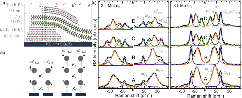
Unpolarized low-frequency Stokes and anti-Stokes Raman scattering spectra measured on the heterostructures under E=1.96 eV excitation are shown in Fig. 1(c). The spectra from regions A comprise two peaks, which are characteristic of atomically thin MoTe2 Froehlicher et al. (2015); Grzeszczyk et al. (2016) or other thin TMD structures Boukhicha et al. (2013); Zhao et al. (2013); Zhang et al. (2013); Kim et al. (2017). The peaks correspond to rigid displacements of whole Te–Mo–Te layers, which are parallel (shear mode - SM) and perpendicular (breathing mode - BM) to the structure plane. Their energies are summarized in Table 1. The BM softens (redshifts) while the SM hardens (blueshifts) with an increasing number of layers. Froehlicher et al. (2015); Grzeszczyk et al. (2016) As a result the BM in 2 L-MoTe2 can be appreciated at higher energy than the SM, while in 3 L-MoTe2 the opposite case takes place. Experimental studies of the low-frequency modes in TMDs confirmed that the energies of the rigid oscillation modes can be well described within a linear chain model. The model considers every layer as a single point mass connected to the nearest neighboring layers with springs, see Fig. 1(b). The interlayer interaction can be described by effective interlayer force constants (j = z for BM or j = x for SM). It is also assumed that the force constant does not depend on the number of layers. Finally, no interaction with the substrate is taken into account in the model. The evolution of the interlayer mode energies (expressed in cm-1) as a function of the number of layers, , is given within the model by Lin and Tan (2019):
| (1) |
where is the respective force constant, is the mass per unit area, ( corresponds to the acoustic mode). The Raman-active SMs (BMs), observed in our experiment belong to the highest-energy (lowest-energy) branches of the corresponding set () and will be hereafter referred to as and for bi- and tri-layer structure, respectively. Assuming that the energy of the BM (SM) in 2 L- and 3 L-MoTe2 in the region A equals correspondingly cm-1 and ( cm-1 and cm-1), the derived force constant value is (). These force constants correspond to our previous results Grzeszczyk et al. (2016) and other published data for MoTe2 ( and , respectively) Froehlicher et al. (2015).
| A | B | C | D | ||||||
| Mode | Energy | Mode | Energy | Mode | Energy | Mode | Energy | ||
| (cm-1) | (cm-1) | (cm-1) | (cm-1) | ||||||
| 2 L | BM | 23.6 | 23.6 | ||||||
| 27.2 | 26.65 | 28.0 | 28.3 | ||||||
| 33.1 | 32.4 | ||||||||
| SM | 19.25 | 19.1 | 19.1 | 19.0 | |||||
| 3 L | BM | 15.35 | 15.2 | ||||||
| 19.0 | 18.4 | 19.25 | 19.6 | ||||||
| SM | 23.3 | 23.4 | 23.4 | 23.4 | |||||
The spectra substantially change, when the layers are placed on the h-BN/SiO2/Si substrate (region D). The SMs in 2 L- and 3 L-MoTe2 are not affected by the presence of the h-BN substrate (see Fig. 1(c)). On the contrary three (two) peaks can be observed in the spectrum measured on the D region as compared to one BM in 2 L- (3 L-) MoTe2/SiO2/Si. Dominant in the 2 L-MoTe2/h-BN/SiO2/Si heterostructure is the feature at cm-1, at the energy slightly higher than the energy of the corresponding BM in the MoTe2/SiO2/Si ( cm-1). The main peak is accompanied by two other peaks cm-1 and cm-1, which emerge at its higher and lower energy sides. Two peaks in the spectrum of 3 L-MoTe2/h-BN/SiO2/Si heterostructure can be observed at the energies cm-1 and cm-1.
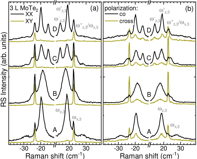
In order to attribute those peaks, polarization-sensitive measurements were performed (see Fig. 2). It is well known, that the BMs have the A–symmetry and the SMs exhibit the E–symmetry Loudon (1964). Therefore, in the backscattering geometry, the BM should not be observed in the (XY) configuration, in which the linear polarization of the scattered light is perpendicular to the linear polarization of the illuminating light, while both the BM and SM can be observed in the co-polarized (XX) configuration. As it can be appreciated in Fig. 2(a), only SM modes are seen in the (XY) configuration from every region of 3 L MoTe2 structure, while all the peaks can be observed in the (XX) configuration. This approach is most commonly used for characterizing symmetry of observed phonon modes. However, the presence of E–symmetry modes for both the co- and cross-polarization configurations may leave some uncertainties in resolving Raman spectra. Thus, in order to fully identify the described peaks, the same measurements have been carried out with circular polarization of light. The helicity-resolved Raman scattering can be a useful tool to distinguish contributions from degenerated modes of different symmetries. In this case, the selection rules ensure that A–symmetry phonons are only visible when helicities of incident and scattered light are the same (co-circular), while opposite situation (cross-circular) takes place for E–symmetry modes. Chen et al. (2015) This prediction is consistent with our results, presented in Fig. 2(b). For region A, the co-circular configuration results in the spectrum dominated by one strong peak, which is assigned as BM (). In the corresponding cross-circular configuration, an additional peak becomes visible, which we assign as SM (). The SM peak can be clearly distinguished in regions C and D for both polarizations, which leads us to assume that we are dealing with two degenerate peaks of different symmetries. The fact that some modes are fairly visible in both polarizations is, in our opinion, the result of the used resonant excitation. It should be noted, however, that the intensity of peaks of a certain symmetry in individual measurements is significantly different. The polarization-resolved results for 3 L MoTe2 structure confirm the attribution of the and modes to the out-of-plane (BM) vibrations, as well as the degeneracy of the third peak, which includes contributions from both and .
No qualitative difference between the spectra measured on the C and D regions of both 2 L and 3 L heterostructures can be noticed in Fig. 1(c). This suggests that the effect of covering the 2 L and 3 L with an h-BN layer is noticeably weaker as compared to the significant influence of the bottom h-BN flakes. In our opinion, this is related to the fabrication process (see SM for details). Consequently, it may be expected that the results obtained on the B regions of the studied heterostructures may resemble those measured on the A-region due to the negligible interaction with the top h-BN layer. Surprisingly, in higher energies, an additional peak can be observed for the B region of the 2L sample. This may be attributed to the non-homogenous interaction between the MoTe2 layer and the top h-BN flake as well as the strain effects due to the roughness of the SiO2/Si substrate (see SM for details). The SM-related features in the B-region spectrum are rather similar to those observed in other (A, C, and D) regions as far as both the energy and the broadening are concerned. Importantly, for both structures, the energy of the main BM-related peaks in the B-region spectra for both 2 L and 3 L structures are slightly lower than those observed in the A region (as well as C and D regions).
It is generally accepted that the interaction of TMDs with the substrate can be neglected Lee, Kim, and Cheong (2015) and slight differences between the low-energy Raman spectra of supported and suspended structures are typically ascribed to strain rather than to the interaction with the substrate O’Brien et al. (2017). However, there are also reports on a substrate-induced mode in the low-frequency spectrum of Bi2Te3 nanoplates Zhao et al. (2014) and a Raman mode splitting in few-layer black phosphorus encapsulated in h-BN Urban et al. (2017).
Let us consider an interaction between the bottommost MoTe2 layer and the substrate, described by the a well-defined force constant . For a bilayer, there are two frequency branches and corresponding to the BMs, with energies given by:
| (2a) | |||
| (2b) |
If equals zero (no interaction with the substrate), the modes correspond to the BM and the acoustic mode, of which only the former one is Raman-active and can be observed in the spectrum. On the other hand, if both modes become Raman active. Theoretical evolution of and with / ratio for several values of force constants is shown in Fig. 3.
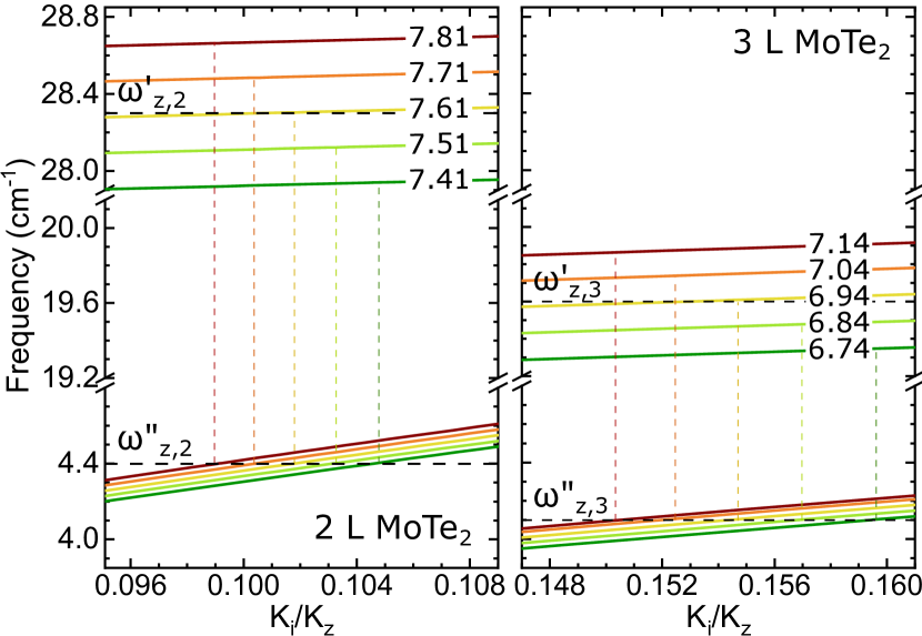
It can be seen that the energy only weakly depends on . The evolution of the lower, energy with the / is much faster, however the energy is rather low for reasonable values of the / ratio. The corresponding peak could be therefore hardly observed in the low-frequency Raman spectrum, as opposite to the reported results for Bi2Te3 and Bi2Se3 crystals Zhao et al. (2014). In our opinion, the vibrational mode contributes to the combination: and modes, which are present in the spectra of the C and D regions of the structure. Assuming cm-1 (an average energy difference between the main BM peak and its satellites) one can get the corresponding /. As it can be appreciated in Fig. 3, the energy of the main peak cm-1, which corresponds to the / value stated above, can be reproduced with . This value corresponds well to the force constant found for the A region of the 2 L MoTe2. The interaction with the substrate can be therefore described with .
Before the same model will be applied to the 3 L-MoTe2 heterostructure, it should be noticed that just two BMs can be observed in the corresponding Raman scattering spectrum, while excited with E=1.96 eV light, as opposite to three peaks in the spectrum of similar 2 L-MoTe2 structure. In fact, if the peak is related to the difference: , the peak related to the sum should be present in the spectrum. The latter mode cannot be distinguished in the E=1.96 eV excited Raman spectrum, as it coincides with the SM in the structure. As was previously stated, the helicity-resolved measurments confirmed the degeneracy of this two phonons (see Fig. 2(b)). This conclusion supports our model with the combined sum and differential modes, and justifies its application to the 3 L-MoTe2 structure. The corresponding equation of motion cannot be solved analytically in that case, so the results of numerical analysis are presented in Fig. 3. Assuming cm-1 one can get the corresponding / cm-1. Finally and can be found in order to reproduce the energy of the main peak cm-1.
We propose the following scenario to explain our results. The bottom MoTe2 interacts with the h-BN substrate in 2 L- and 3 L-MoTe2. Because of the high uniformity of the substrate (see SM for the AFM topography), the resulting vibrational mode has a well-defined vibration frequency and contributes to the combination of Raman modes, as can be seen in the spectra. Therefore, crucial for the effect of encapsulation is the h-BN substrate, which provides a flat support for the TMD layer Jadczak et al. (2019); Kang et al. (2019). This minimizes the effect of strain and disorder resulting from the roughness of the SiO2/Si substrate. The resemblance of the spectra from regions C and D suggests that the top h-BN layer does not strongly interact with the MoTe2 layers but rather provides protection from ambient conditions Son et al. (2017); Lee et al. (2015). The results from region B can also be addressed within our model. Characteristic of both the 2 L- and 3 L-MoTe2 case is the lowering of the main BM peak energy as compared to the uncovered structures. The energy redshifts suggest the presence of substantial strain in the structure. As schematically shown in Fig. 1(a), the region B is not uniform and the deformation can change from point to point.
Our model does not address all features of the presented results. The force constants, which could be used to reproduce the observed Raman spectra seem to depend on the number of layers, however, the experimental uncertainty can be partially responsible for the effect. It is important to mention that similar results devoted to the interaction effects between a substrate and a TMD layer were reported for WS2/h-BN structures. Lin et al. (2019) The authors shown that the reduced symmetry of heterostructures leads to the activation of new interlayer phonons in the Raman spectra. Those modes could be observed due to their intensity enhancement resulting from the resonance of the excitation with the specific excitonic transition in WS2.
In conclusion, the effect of h-BN encapsulation on the low-frequency Raman scattering in 2 L- and 3 L-MoTe2 has been investigated. Three BMs have been observed in the spectra of few-layer MoTe2 deposited on/encapsulated in h-BN as compared to one mode for the flake deposited on SiO2/Si. The additional satellite peaks have been assigned to the two-phonon scattering effect. The SM does not seem to be affected by changing the substrate. The results have been analyzed in terms of a linear chain model. The observation has been explained by introducing to the model a well-defined interaction between the lowest MoTe2 layer and the h-BN substrate. The interaction slightly affects the energy of the main BM and activates an otherwise inactive, zero-frequency acoustic mode. The latter mode cannot be directly observed in the spectrum but it contributes to the combination modes in a MoTe2 structure.
Supplementary Material
See supplementary material for experimental details, AFM analysis, Raman spectra in non-resonant regime and data from other samples.
Acknowledgements.
The work has been supported by the National Science Center, Poland (grant no. 2017/27/B/ST3/00205, 2017/27/N/ST3/01612, 2017/24/C/ST3/00119), the ATOMOPTO project (TEAM programme of the Foundation for Polish Science co-financed by the EU within the ERDFund), EU Graphene Flagship project (ID: 785219) and Ministry of Education, Youth and Sports of the Czech Republic under the project CEITEC 2020 (LQ1601).AIP Publishing Data sharing policy
The data that support the findings of this study are available from the corresponding author upon reasonable request.
The following article has been accepted by Applied Physics Letters. After it is published, it will be found at https://dx.doi.org/10.1063/1.5128048
References
- Radisavljevic et al. (2011) B. Radisavljevic, A. Radenovic, J. Brivio, V. Giacometti, and A. Kis, “Single-layer MoS2 transistors,” Nature Nanotechnology 6, 147 (2011).
- Choi et al. (2013) M. S. Choi, G.-H. Lee, Y.-J. Yu, D.-Y. Lee, S. H. Lee, P. Kim, J. Hone, and W. J. Yoo, “Controlled charge trapping by molybdenum disulphide and graphene in ultrathin heterostructured memory devices,” Nature Communications 4, 1624 (2013).
- Wang et al. (2012) H. Wang, L. Yu, Y.-H. Lee, Y. Shi, A. Hsu, M. L. Chin, L.-J. Li, M. Dubey, J. Kong, and T. Palacios, “Integrated circuits based on bilayer MoS2 transistors,” Nano Letters 12, 4674–4680 (2012).
- Zhou and Zhao (2016) S. Zhou and J. Zhao, “Electronic structures of germanene on MoS2: effect of substrate and molecular adsorption,” The Journal of Physical Chemistry C 120, 21691–21698 (2016).
- Ajayi et al. (2017) O. A. Ajayi, J. V. Ardelean, G. D. Shepard, J. Wang, A. Antony, et al., “Approaching the intrinsic photoluminescence linewidth in transition metal dichalcogenide monolayers,” 2D Materials 4, 031011 (2017).
- Tongay et al. (2013) S. Tongay, J. Zhou, C. Ataca, J. Liu, J. S. Kang, T. S. Matthews, L. You, J. Li, J. C. Grossman, and J. Wu, “Broad-range modulation of light emission in two-dimensional semiconductors by molecular physisorption gating,” Nano Letters 13, 2831–2836 (2013).
- Su et al. (2015) L. Su, Y. Yu, L. Cao, and Y. Zhang, “Effects of substrate type and material-substrate bonding on high-temperature behavior of monolayer WS2,” Nano Research 8, 2686–2697 (2015).
- Lee et al. (2015) G.-H. Lee, X. Cui, Y. D. Kim, G. Arefe, X. Zhang, C.-H. Lee, F. Ye, K. Watanabe, T. Taniguchi, P. Kim, et al., “Highly stable, dual-gated MoS2 transistors encapsulated by hexagonal boron nitride with gate-controllable contact, resistance, and threshold voltage,” ACS Nano 9, 7019–7026 (2015).
- Cao et al. (2015) Y. Cao, A. Mishchenko, G. Yu, E. Khestanova, A. Rooney, et al., “Quality heterostructures from two-dimensional crystals unstable in air by their assembly in inert atmosphere,” Nano Letters 15, 4914–4921 (2015).
- Ahn et al. (2016) S. Ahn, G. Kim, P. K. Nayak, S. I. Yoon, H. Lim, H.-J. Shin, and H. S. Shin, “Prevention of transition metal dichalcogenide photodegradation by encapsulation with h-BN layers,” ACS Nano 10, 8973–8979 (2016).
- Cadiz et al. (2017) F. Cadiz, E. Courtade, C. Robert, G. Wang, Y. Shen, H. Cai, T. Taniguchi, K. Watanabe, H. Carrere, D. Lagarde, et al., “Excitonic linewidth approaching the homogeneous limit in MoS2-based van der Waals heterostructures,” Physical Review X 7, 021026 (2017).
- Molas et al. (2019) M. R. Molas, A. O. Slobodeniuk, K. Nogajewski, M. Bartos, L. Bala, A. Babiński, K. Watanabe, T. Taniguchi, C. Faugeras, and M. Potemski, “Energy spectrum of two-dimensional excitons in a nonuniform dielectric medium,” Phys. Rev. Lett. 123, 136801 (2019).
- Cui et al. (2014) X. Cui, G.-H. Lee, Y. D. Kim, G. Arefe, P. Y. Huang, C.-H. Lee, D. A. Chenet, X. Zhang, L. Wang, F. Ye, et al., “Multi-terminal electrical transport measurements of molybdenum disulphide using van der Waals heterostructure device platform,” arXiv preprint arXiv:1412.5977 (2014).
- Mayorov et al. (2011) A. S. Mayorov, R. V. Gorbachev, S. V. Morozov, L. Britnell, R. Jalil, L. A. Ponomarenko, P. Blake, et al., “Micrometer-scale ballistic transport in encapsulated graphene at room temperature,” Nano letters 11, 2396–2399 (2011).
- Lee, Kim, and Cheong (2015) J.-U. Lee, K. Kim, and H. Cheong, “Resonant Raman and photoluminescence spectra of suspended molybdenum disulfide,” 2D Materials 2, 044003 (2015).
- Froehlicher et al. (2015) G. Froehlicher, E. Lorchat, F. Fernique, C. Joshi, A. Molina-Sánchez, L. Wirtz, and S. Berciaud, “Unified description of the optical phonon modes in N-layer MoTe2,” Nano Letters 15, 6481–6489 (2015).
- Grzeszczyk et al. (2016) M. Grzeszczyk, K. Gołasa, M. Zinkiewicz, K. Nogajewski, M. Molas, M. Potemski, A. Wysmołek, and A. Babiński, “Raman scattering of few-layers MoTe2,” 2D Materials 3, 025010 (2016).
- Boukhicha et al. (2013) M. Boukhicha, M. Calandra, M.-A. Measson, O. Lancry, and A. Shukla, “Anharmonic phonons in few-layer MoS2: Raman spectroscopy of ultralow energy compression and shear modes,” Physical Review B 87, 195316 (2013).
- Zhao et al. (2013) Y. Zhao, X. Luo, H. Li, J. Zhang, P. T. Araujo, C. K. Gan, J. Wu, H. Zhang, S. Y. Quek, M. S. Dresselhaus, et al., “Interlayer breathing and shear modes in few-trilayer MoS2 and WSe2,” Nano letters 13, 1007–1015 (2013).
- Zhang et al. (2013) X. Zhang, W. Han, J. Wu, S. Milana, Y. Lu, Q. Li, A. C. Ferrari, and P. Tan, “Raman spectroscopy of shear and layer breathing modes in multilayer MoS2,” Physical Review B 87, 115413 (2013).
- Kim et al. (2017) S. Kim, K. Kim, J.-U. Lee, and H. Cheong, “Excitonic resonance effects and davydov splitting in circularly polarized Raman spectra of few-layer WSe2,” 2D Materials 4, 045002 (2017).
- Lin and Tan (2019) M.-L. Lin and P.-H. Tan, “Ultralow-frequency Raman spectroscopy of two-dimensional materials,” in Raman Spectroscopy of Two-Dimensional Materials (Springer, 2019) pp. 203–230.
- Loudon (1964) R. Loudon, “The Raman effect in crystals,” Advances in Physics 13, 423–482 (1964).
- Chen et al. (2015) S.-Y. Chen, C. Zheng, M. S. Fuhrer, and J. Yan, “Helicity-resolved Raman scattering of MoS2, MoSe2, WS2, and WSe2 atomic layers,” Nano letters 15, 2526–2532 (2015).
- O’Brien et al. (2017) M. O’Brien, N. Scheuschner, J. Maultzsch, G. S. Duesberg, and N. McEvoy, “Raman spectroscopy of suspended MoS2,” Physica Status Solidi (B) 254, 1700218 (2017).
- Zhao et al. (2014) Y. Zhao, X. Luo, J. Zhang, J. Wu, X. Bai, M. Wang, J. Jia, H. Peng, Z. Liu, S. Y. Quek, et al., “Interlayer vibrational modes in few-quintuple-layer Bi2Te3 and Bi2Se3 two-dimensional crystals: Raman spectroscopy and first-principles studies,” Physical Review B 90, 245428 (2014).
- Urban et al. (2017) J. Urban, M. Baranowski, A. Surrente, D. Wlodarczyk, A. Suchocki, et al., “Observation of A1g Raman mode splitting in few layer black phosphorus encapsulated with hexagonal boron nitride,” Nanoscale 9, 19298–19303 (2017).
- Jadczak et al. (2019) J. Jadczak, L. Bryja, J. Kutrowska-Girzycka, P. Kapuściński, M. Bieniek, Y.-S. Huang, and P. Hawrylak, “Room temperature multi-phonon upconversion photoluminescence in monolayer semiconductor WS2,” Nature Communications 10, 107 (2019).
- Kang et al. (2019) J.-W. Kang, J.-W. Jung, T. Lee, J. G. Kim, and C.-H. Cho, “Enhancing exciton diffusion in monolayer WS2 with h-BN bottom layer,” Physical Review B 100, 205304 (2019).
- Son et al. (2017) S.-K. Son, M. Šiškins, C. Mullan, J. Yin, V. G. Kravets, A. Kozikov, S. Ozdemir, M. Alhazmi, M. Holwill, K. Watanabe, et al., “Graphene hot-electron light bulb: incandescence from hBN-encapsulated graphene in air,” 2D Materials 5, 011006 (2017).
- Lin et al. (2019) M.-L. Lin, Y. Zhou, J.-B. Wu, X. Cong, X.-L. Liu, J. Zhang, H. Li, W. Yao, and P.-H. Tan, “Cross-dimensional electron-phonon coupling in van der Waals heterostructures,” Nature Communications 10, 2419 (2019).
Supplementary Material:
Breathing modes in few-layer MoTe2 activated by h-BN encapsulation
M. Grzeszczyk,1 M. R. Molas,1 M. Bartoš,2,3 K. Nogajewski,1 M. Potemski,1,2 A. Babiński1
1)Institute of Experimental Physics, Faculty of Physics, University of Warsaw, ul.
Pasteura 5, 02-093 Warsaw,
Poland
2)Laboratoire National des Champs Magnétiques Intenses, CNRS-UGA-UPS-INSA-EMFL, 25, avenue des Martyrs,
38042 Grenoble, France
3)Central European Institute of Technology, Brno University of Technology, Purkyňova 656/123, 612 00 Brno, Czech
Republic
S1 Sample fabrication
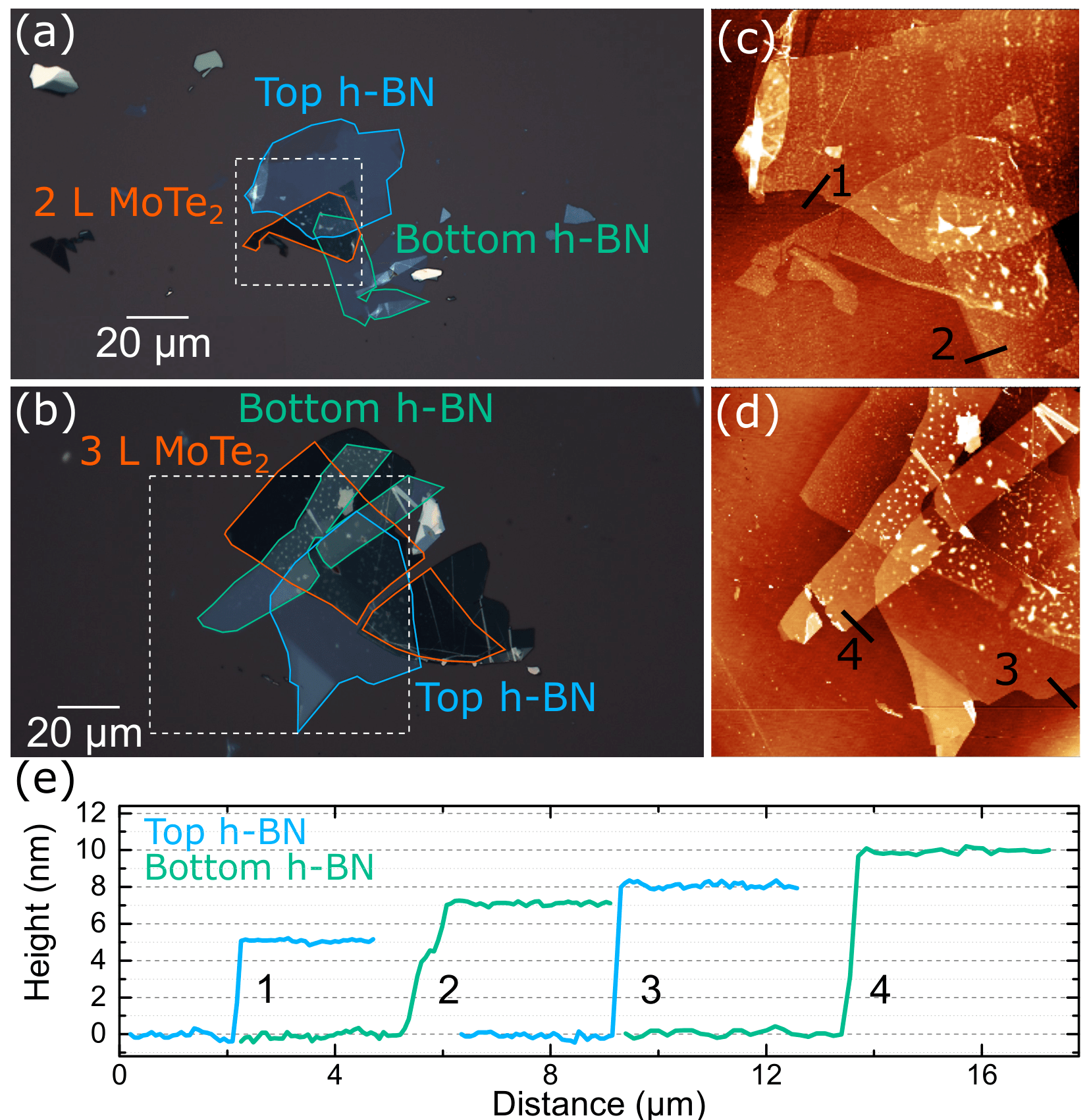
Investigated samples comprised of thin MoTe2 and h-BN layers fabricated by two-stage PDMS-based mechanical exfoliation of bulk crystals purchased from HQGraphene. As a substrate, a SiO2 (90 nm)/Si wafer was used. In order to ensure the best quality of the substrate surface, they were first cleaned (placed in acetone in the ultrasonic washer then rinsed in isopropanol and deionized water) and annealed at 200∘C. They were kept on hot-plate until the first non-deterministic transfer of h-BN flakes. This procedure minimizes the occurrence of air pockets and ensures good adhesion between the flake and the substrate. It should be underlined that subsequent layers were transferred deterministically, which adds the possibility of additional contaminants on the interfaces between the constituent layers. In an attempt to reduce inhomogeneities between each transfer, the sample was annealed. The 2 L- and 3 L-MoTe2 flakes were placed on the surface partially on top of the SiO2 (90 nm)/Si substrate and partially on the h-BN layer. Such heterostructures were partially capped with top h-BN flakes. The complete structures were annealed at 120∘C for 1.5 hour in order to ensure the best layer-to-layer and layer-to-substrate adhesion and to eliminate a substantial portion of air pockets at interfaces between the constituent layers.
Fig. S1(a)-(b). presents an optical microscope image of the investigated heterostructures. The sample topography, as measured by atomic force microscopy, is shown in Fig. S1(c)-(d). Height profile measurements (performed along straight lines marked in (c)-(d)), which were performed in order to unambiguously determine the thickness of layers, are presented in Fig. S1(e). The top h-BN layer was 5 nm (8 nm) thick and the bottom h-BN layer was 7 nm (10 nm) thick in the 2 L- (3 L) case.
S2 Surface roughnesses of substrates
In the left-hand side panel of Fig. S2 the AFM image of an h-BN flake non-deterministically transferred on Si/SiO2 substrate is shown. The Figure illustrates the effect of substrate on the studied material. To quantify the roughness of both surfaces, we show the corresponding height profiles measured on the hBN flakes and the SiO2 substrate. As it can be seen in the Figure, the surface roughness of the Si/SiO2 substrate is significantly larger as compared to the h-BN flake, which can be seen as much larger variation of heights of the Si/SiO2 (almost 2 nm) as compared to the h-BN (about 0.5 nm). This confirms that h-BN thick layers can work as atomically flat substrates, which is consistent with previous reports. xue2011scanning ; quereda2014single In the right-hand side panel of Fig. S2 the corresponding phase image is shown. That powerful extension of AFM tapping mode is very sensitive to local variations in the material properties boussu2005roughness ; magonov1997phase and it is often used for its superior contrast of nanoscale features. The presented results demonstrate the difference in topography of Si/SiO2 and h-BN surfaces. The strong contrast variation clearly reveals the non-uniform nature of the SiO2 surface.
S3 Experimental setup
Raman scattering measurements were carried out in the backscattering geometry using 1.96 eV excitation from a He-Ne laser and 2.41 eV excitation from an Ar+ ion laser. The excitation light was focused by means of a 100x magnification long working distance objective. The spot diameter of the focused beam was equal to about 1 m. The excitation power focused on the sample was kept at 80 W during all measurements to avoid local heating. The scattered light was collected via the same microscope objective, sent through a 1 m monochromator and detected with a liquid-nitrogen cooled CCD camera. To detect low-energy Raman scattering up to about 10 cm-1 from the laser line, a set of Bragg filters were implemented in both excitation and detection paths. The linear polarization of the measured signal was analyzed using a set of polarizers and a half-waveplate, while for helicity resolved measurements additionally a quarter-wave plate was implemented.
S4 Supplementary Raman spectra of MoTe2 flakes.
S4.1 Non-resonant Raman scattering
The overall lineshape of the low-frequency Raman spectrum strongly depends on the excitation energy, which is related to resonance effects yang2017 . In particular, we previously observed, that the SM in few-layer MoTe2 is very weak in the non-resonant Raman scattering spectrum. grzeszczyk2016 The spectra measured with E=2.41 eV excitation in this experiment are shown in Fig. S3. The SMs can be hardly seen in the spectrum from the A region, while the expected peak can be distinguished in the spectra from the C and D regions of the 3 L-MoTe2 heterostructure.
S4.2 MoTe2 flakes covered with h-BN
In an attempt to better understand the results observed in the B region, another sample with 2 L MoTe2 covered with thin top h-BN flake was fabricated. As it is presented in Fig. S4, one can easily find areas in which the additional peak is not visible due to the bigger size of the sample.
S4.3 Fully encapsulated samples
The low-energy Raman spectra of MoTe2 thin layers from a monolayer (1 L) to trilayer (3 L) are shown in Fig. S5. The spectra were measured on two different samples: as deposited on Si/SiO2 substrate and encapsulated in h-BN flakes. Note that this sample was fabricated and investigated prior to the structures studied in the main text. To describe the presented Raman spectra, we can start the analysis with the results obtained for 1 L. As can be seen in the Figure, there are no observed low-energy mode is present in both structures. It is well known, that no rigid interlayer vibrations in the case of a monolayer are expected if the interaction between the monolayer and the substrate is neglected lee2015 ; froehlicher2015 ; grzeszczyk2016 . As we discuss in the main text, the structure-substrate interaction leads to the activation of the acoustic mode, which consequently should be observed in the Raman spectrum. Our predictions suggest that its energy is of about 5 cm-1 (see Fig. 3 in the main). However, we were not able to detect it as the used Bragg filter allows to measure a signal of around cm-1 from a laser line. The results obtained for 2 L and 3 L show that there is a significant effect of the h-BN flakes on their Raman spectra. The observed structures of breathing modes in h-BN encapsulated layers are very similar to the ones presented in Fig. 2 in the main text. Particularly, a triple structure of breathing modes can be observed straightforward for a bilayer encapsulated in h-BN. The thicknesses of the bottom h-BN flake for the studied encapsulated MoTe2 layers shown in Fig. S5 differs from the that of the samples described in the main text (100 nm versus 10 nm). This suggests that the thickness of h-BN flakes does not affect the apparent structure of breathing modes (three peaks). However, as it can be noted, their thickness may influence the measured intensity of phonon modes due to the occurred interference-effect.
S5 Linewidth of the main breathing modes in Raman spectra

Fig. S6 illustrates the change of the linewidth of main Raman modes / and / measured on the heterostructures. For both samples a significant decrease of the FWHM can be observed from spot A to spot D. For pristine MoTe2 flake linewidth of the peak equals 7 cm-1(5 cm-1) for 2 L (3 L) thickness. After covering the flake with the h-BN layer this value is decreasing. This behavior can be understood in terms of surface quality. High roughness of the Si/SiO2 substrate leads to the inhomogeneous broadening of the Raman peaks. As was previously shown in Section S2, h-BN flakes have much flatter surfaces. Capping MoTe2 with the h-BN layer improves the quality of its surface, and as a result, the narrowing of the phonon peak can be observed. This effect is most evident in the C and D areas, where MoTe2 flake is placed on the h-BN layer. In this case, atomically flat substrates lead to the peak’s linewidth reduction by half. Our reasoning can explain the decrease of the linewidth between A, B, and C areas. However, we see a further drop in the peak’s FWHM between C and D areas in both structures. This result is not surprising. As it was mentioned before h-BN can be considered as atomically flat substrates. The good adhesion between h-BN and MoTe2 is also induced by our fabrication process. The interface between the top h-BN layer and MoTe2 is of considerably lower quality. Our result reveals the presence of strain and many air-pockets in part of the samples with h-BN capping layer. These impurities and defects add to the broadening of the phonon linewidth.
References
- (1) J. Xue, J. Sanchez-Yamagishi, D. Bulmash, P. Jacquod, A. Deshpande, K. Watanabe, T. Taniguchi, P. Jarillo-Herrero, and B. J. LeRoy, “Scanning tunnelling microscopy and spectroscopy of ultra-flat graphene on hexagonal boron nitride,” Nature Materials 10, 282 (2011).
- (2) J. Quereda, A. Castellanos-Gomez, N. Agraït, and G. Rubio-Bollinger, “Single-layer MoS2 roughness and sliding friction quenching by interaction withatomically flat substrates,” Applied Physics Letters 105, 053111 (2014).
- (3) K. Boussu, B. Van der Bruggen, A. Volodin, J. Snauwaert, C. Van Haesendonck, and C. Vandecasteele, “Roughness and hydrophobicity studies of nanofiltration membranes using different modes of AFM,” Journal of colloid and interface science 286, 632–638 (2005).
- (4) S. Magonov, V. Elings, and M.-H. Whangbo, “Phase imaging and stiffness in tapping-mode atomic force microscopy,” Surface Science 375, L385–L391 (1997).
- (5) J. Yang, J.-U. Lee, and H. Cheong, “Excitation energy dependence of Raman spectra of few-layer WS2,” FlatChem 3, 64–70 (2017).
- (6) M. Grzeszczyk, K. Gołasa, M. Zinkiewicz, K. Nogajewski, M. Molas, M. Potemski, A. Wysmołek, and A. Babiński, “Raman scattering of few-layers MoTe2,” 2D Materials 3, 025010 (2016).
- (7) J.-U. Lee, K. Kim, and H. Cheong, “Resonant Raman and Photoluminescence spectra of suspended molybdenum disulfide,” 2D Materials 2, 044003 (2015).
- (8) G. Froehlicher, E. Lorchat, F. Fernique, C. Joshi, A. Molina-Sánchez, L. Wirtz, and S. Berciaud, “Unified description of the optical phonon modes in N-layer MoTe2,” Nano Letters 15, 6481–6489 (2015).