High-energy optical transitions and optical constants of \ceCH3NH3PbI3 measured by spectroscopic ellipsometry and spectrophotometry
Abstract
Optoelectronics based on metal halide perovskites (MHPs) have shown substantial promise, following more than a decade of research. For prime routes of commercialization such as tandem solar cells, optical modeling is essential for engineering device architectures, which requires accurate optical data for the materials utilized. Additionally, a comprehensive understanding of the fundamental material properties is vital for simulating the operation of devices for design purposes. In this article, we use variable angle spectroscopic ellipsometry (SE) to determine the optical constants of \ceCH3NH3PbI3 (MAPbI3) thin films over a photon energy range of 0.73 to 6.45 eV. We successfully model the ellipsometric data using six Tauc-Lorentz oscillators for three different incident angles. Following this, we use critical-point analysis of the complex dielectric constant to identify the well-known transitions at 1.58, 2.49, 3.36 eV, but also additional transitions at 4.63 and 5.88 eV, which are observed in both SE and spectrophotometry measurements. This work provides important information relating to optical transitions and band structure of MAPbI3, which can assist in the development of potential applications of the material.
keywords:
American Chemical Society, LaTeXUniversity of Southampton] Physics and Astronomy department, University of Southampton, University Road, Southampton, SO17 1BJ University of Southampton] Physics and Astronomy department, University of Southampton, University Road, Southampton, SO17 1BJ University of Southampton] Physics and Astronomy department, University of Southampton, University Road, Southampton, SO17 1BJ \alsoaffiliation[Skoltech] Skolkovo Institute of Science and Technology (Skoltech), Skolkovo, Moscow, Russia, 121205 \abbreviationsIR,NMR,UV
1 Introduction
Metal halide perovskites (MHPs) are a propitious group of materials for thin-film optoelectronics, with the research field still thriving and record solar cell efficiencies now reaching greater than 25%.1 As photovoltaic devices begin to approach the theoretical efficiency limit for a single junction 2, 3, 4, 5, fine-tuning of the device structure is required for further optimization. This can only be feasible with the assistance of optical simulations, which require accurate knowledge of the optical properties of device layers. Moreover, one of the most promising applications for commercialization of MHPs are tandem solar cells, where the design also requires extensive optical modeling. 6, 7, 8, 9 The archetypal material for studying the properties of MHPs is \ceCH3NH3PbI3 (MAPbI3), which has been characterised scrupulously, revealing remarkable fundamental features for optoelectronics including high absorption coefficients (– cm-1 at 2 eV)10, 11, 12, 13, low exciton binding energies 14, 15, 16, 17, and small charge-carrier effective masses. 14, 18, 19 As a result, many other optoelectronic applications of MHPs have been developed, including lasers 20, 21, 22, 23, 24, 25, light emitting diodes (LEDs) 26, 27, 28, 29 and photodetectors 30, 31, 32.
Many studies have also been made to characterize the optical constants of MAPbI3 thin films 33, 34, 35, 36, 37, 38, 39, 40, 41, 10, 42, 43, 44, 45, 46, and also other MHPs 47, 48, 49, 50, 51, 52, 53 with varying results and analysis protocols. Optical constants are typically determined by fitting data from spectroscopic ellipsometry (SE) measurements to a dispersion model, which can then be compared with results from spectrophotometry (reflectance and transmission spectroscopy). With spectrophotometry measurements on MHPs, data for wavelengths of nm (photon energies of eV) is usually omitted. This may be due to a) limitations of the measurement range of the equipment used, b) strong absorption of glass substrates and/or c) strong absorption of the material (for thicker films and single crystals), with the latter two resulting in a weak (noisy) signal for optical transmission. Hence, optical transitions at these photon energies are seldom discussed. Nevertheless, studies of this part of the spectrum are important for validating theoretical work regarding the band structure and ultimately understanding the fundamental properties of MHPs. Often the focus of band-structure calculations is to reproduce the bandgap energy of MHPs, however an accurate model should predict spectral features at all photon energies observable by experiment.
Here we use variable angle SE to determine the optical constants of a MAPbI3 thin film over a wide spectral range. The ellipsometric data is modeled using Tauc-Lorentz oscillators for measurements from three different incident angles. We report on several optical transitions which are observed at ultraviolet photon energies in both SE data and spectrophotometry measurements. We present a simple step-by-step approach that can be used for utilizing SE as a method for accurately determining the optical constants, thickness and surface roughness of MHP thin films.
2 Results and discussion
We prepare MAPbI3 via a one-step, gas-assisted spin coating method to achieve smooth uniform thin films.54 This technique utilizes the high pressure flow of inert gas on the surface of the film during the coating process, bypassing the need for anti-solvent quenching.55, 56, 57 We use a precursor of PbI2 and methylammonium iodide (MAI) (1:1) in a mixed solvent solution of DMF and DMSO at a concentration of 1M. Figure 1 shows the sample morphology from atomic force microscopy (AFM) and scanning electron microscopy (SEM). The film has a relatively uniform surface with grain size of 100 to 200 nm.
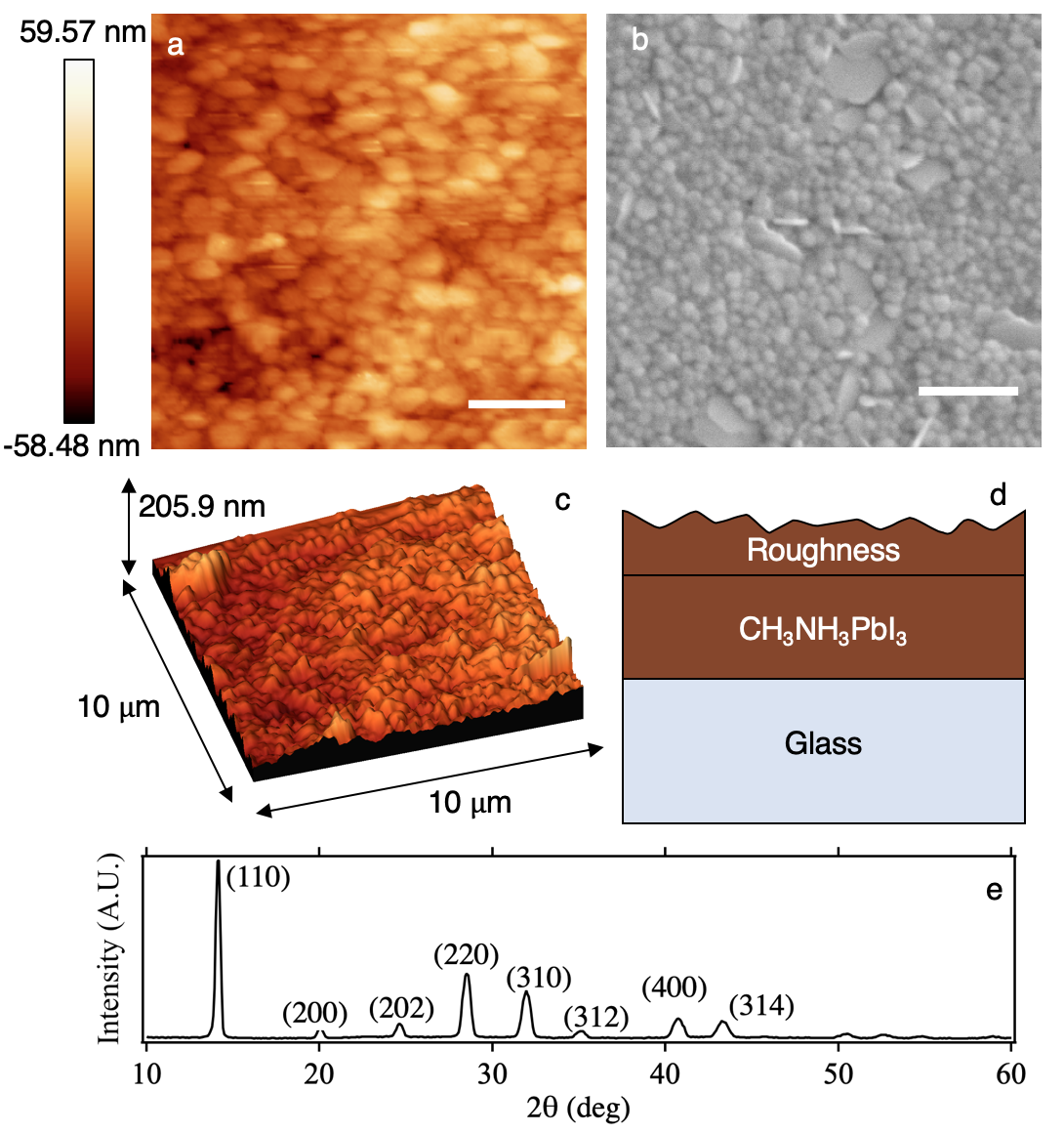
We performed SE measurements on thin films of MAPbI3 to obtain the and values over the spectral range of 192 to 1696 nm, for three angles of incidence (65°, 70°, and 75°). The parameter is the induced phase difference between the - and - polarized light and is the angle whose tangent is given by the ratio of the magnitudes of the reflection coefficients, and for the and polarization planes, respectively, i.e. . We ensure that the sample is measured immediately following exposure to ambient conditions, after being packaged in an inert environment so that minimal degradation occurs prior to measurement. Figure 1e shows the X-ray diffraction pattern of the film in this condition, displaying a high degree of crystallinity and absence of peaks that indicate degradation. To model the ellipsometry results, we firstly use a Cauchy film model to fit the data in the transparent region ( 800 nm), where oscillations due to interference are observed. The refractive index from the Cauchy dispersion model is given by:
| (1) |
where , and are the Cauchy coefficients to be fitted, and is the wavelength. This gives a good estimate for the thickness of the film, which is not fitted during the next phase. Subsequently, the Cauchy film model is parameterized to convert it to a basis-spline (b-spline) model which is used to fit the transparent region of the spectrum. The fit is then expanded to wavelengths below the bandgap, where the film is absorbing. The b-Spline model is then forced to be consistent with Kramers-Kronigs relations and fit to the data once again with updated parameters. Finally, the b-Spline model is parameterized to build an oscillator model with six Tauc-Lorentz oscillators. In the Tauc-Lorentz model, the imaginary part of the dielectric constant is given by
| (2) |
Here, is the bandgap, used as a coupled fitting parameter across all oscillators. The parameter is the amplitude and is the broadening of each oscillator peak centered at the energy . Once the parameters for are obtained, is found using the analytic solution of the Kramers-Kronig integration. 58 The resulting model for pseudo-optical constants can be fitted to the data for and using
| (3) |
where is the angle of incidence and is the induced polarization change (). The parameters are fitted globally for three angles of incidence (65°, 70°, and 75°) over the wavelength range of 192 to 1696 nm. We incorporated the film thickness and surface roughness in the model (Figure 1d) and all parameters are updated to obtain the lowest possible MSE (mean squared error).
The and data is shown in Figure 2, along with the fit from the Tauc-Lorentz oscillator model.
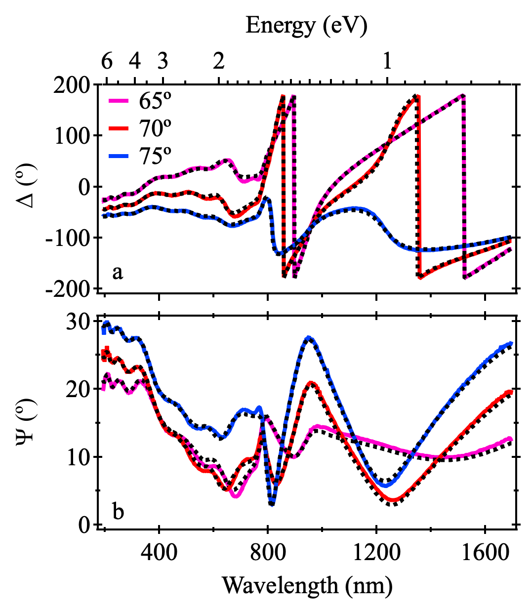
A MSE value of 12.50 is achieved, indicating excellent agreement between the model and data. We obtain a thickness value of 446.84 0.24 nm, which is in agreement of the thickness obtained using profilometry (452 20 nm). The roughness of the film is found to be 10 nm, which is also close to the RMS (root mean square) roughness value of 13 nm obtained by AFM (Figure 1a and c). It is important to factor the surface roughness, since it has a substantial impact on the determination of optical characteristics of the film, with larger values causing erroneous interpretation 59. The fitting parameters obtained from the Tauc-Lorentz model are outlined in Table 1.
| Oscillator | Center (eV) | (eV) | |
|---|---|---|---|
| () | 1.565 0.0046 | 0.127 0.0043 | 99.391 5.8436 |
| 2.535 0.0173 | 0.918 0.0637 | 13.381 3.4237 | |
| 3.390 0.0057 | 0.948 0.0334 | 4.931 0.8600 | |
| 4.665 0.0183 | 1.300 0.0889 | 5.974 0.6147 | |
| 5.790 0.0332 | 1.083 0.1359 | 3.899 0.8210 | |
| 6.521 0.0773 | 0.615 0.2366 | 1.552 0.8695 | |
| 7.674 0.2404 | 46.300 7.4674 |
We find that six oscillators are required to minimize the MSE of the fit and reproduce the data accurately. If fewer than six oscillators are used (four or five, for example), the fit does not capture all of the features of the and curves (Figure 2a and b, respectively) and instead converges to oscillator parameters that provide an average value to account for several transitions. Only very slight reductions in the MSE can be obtained if more oscillators are used, and the amplitude of the additional oscillators have to be very low to achieve this. Therefore, we can conclude that any more or fewer than six main oscillators appears to create a non-physical model. A value of is fitted to provide a dielectric constant at high energies, in order to prevent from becoming zero following the application of the Kramers-Kronig transformation. The element is also included as an unbroadened oscillator to account for high-energy absorption, which effectively provides a ’tilt’ to the dielectric constant. The bandgap value of eV is determined as a coupled fitting parameter for all oscillators.
The optical constants determined from the analysis are presented in Figure 3.
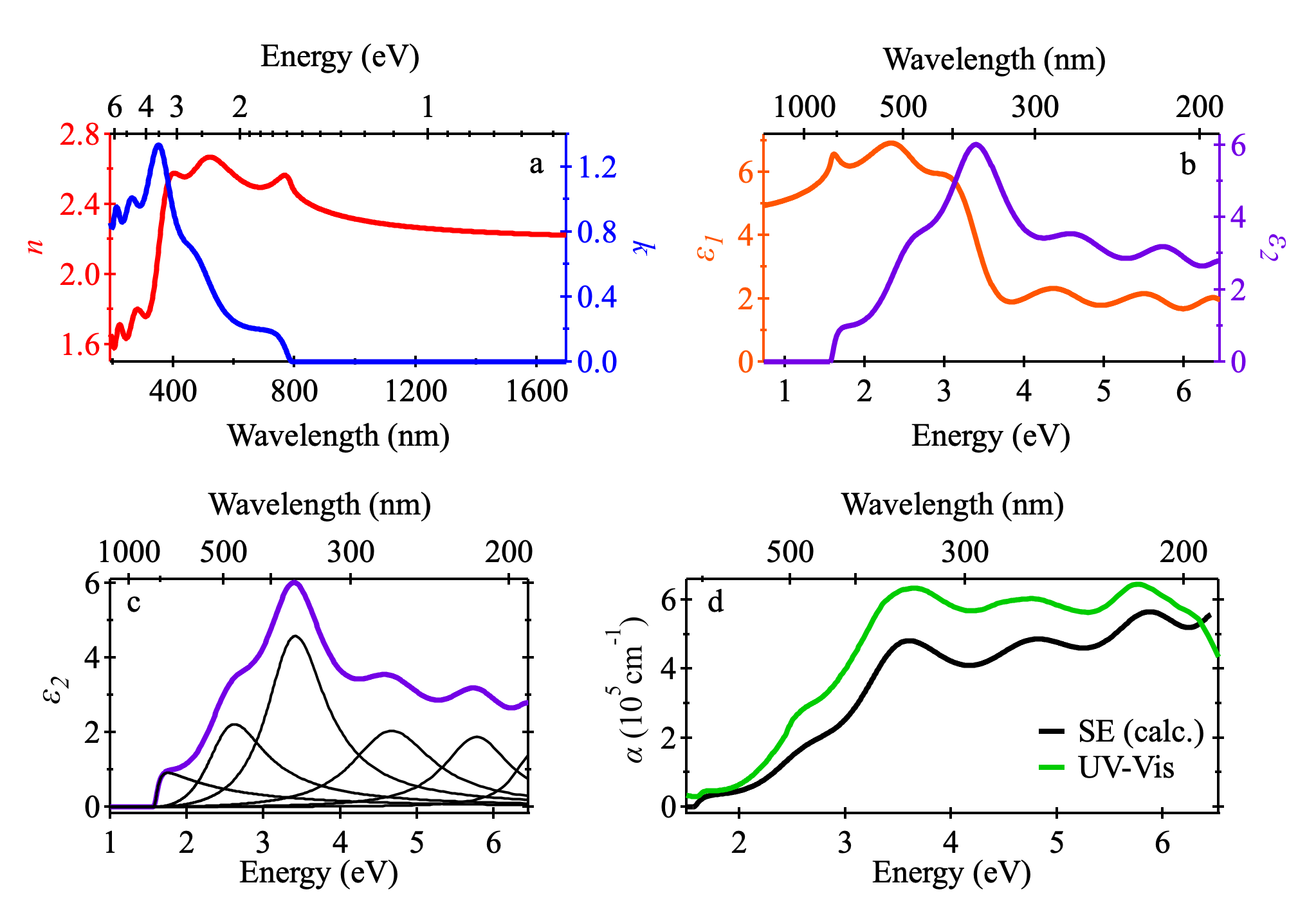
The black curves in Figure 3c show the individual contribution from the Tauc-Lorentz oscillators to . Figure 3d shows the absorption coefficient, derived from the extinction coefficient, , calculated using the relation . We performed spectrophotometry measurements on a different MAPbI3 thin film deposited on quartz to obtain an estimate for the absorption coefficient, which is overlaid with the calculated absorption coefficient in Figure 3d. For these measurements, a thinner film was deposited using a 0.5M solution to obtain a thickness of 110 nm, to ensure the transmission signal was strong enough to be detected at highly absorbing wavelengths.
The observed transitions in the absorbing region of the experimental spectrum appear to corroborate with the modeled data from the ellipsometry measurements. For the SE-calculated absorption coefficient, the value at 2 eV is 4.6 x cm-1, which is in good agreement with previous work.41, 35, 12 The absolute amplitude of the absorption coefficient obtained from spectrophotometry should not be considered as an accurate value for comparison, since scattered light from the sample is not accounted for. Instead, we use the data to compare the shape and position of the optical transitions. One major difference between the two absorption coefficients is position and relative amplitude of the highest energy peak. In the spectrophotometry data, it appears that the two highest energy peaks coincide, creating a high energy shoulder at 6.3 eV in the peak observed with a maximum at 5.8 eV. In the SE data however, it appears that the highest energy peak is blueshifted in comparison, with the maximum lying outside of the measurement range, with the Tauc Lorentz oscillator associated with this peak centered at 6.52 eV (Table 1).
To investigate the optical transitions in MAPbI3, we used critical-point (CP) analysis to accurately determine the transition energies. The CP model gives the following expression for the second derivative of the complex dielectric constant for any given excitonic transition, :
| (4) |
The energy of the transition is given by , the broadening is , the amplitude is , the phase is , and is the imaginary unit. This equation is used to fit the real and imaginary parts of the dielectric function, as shown in Figure 4.
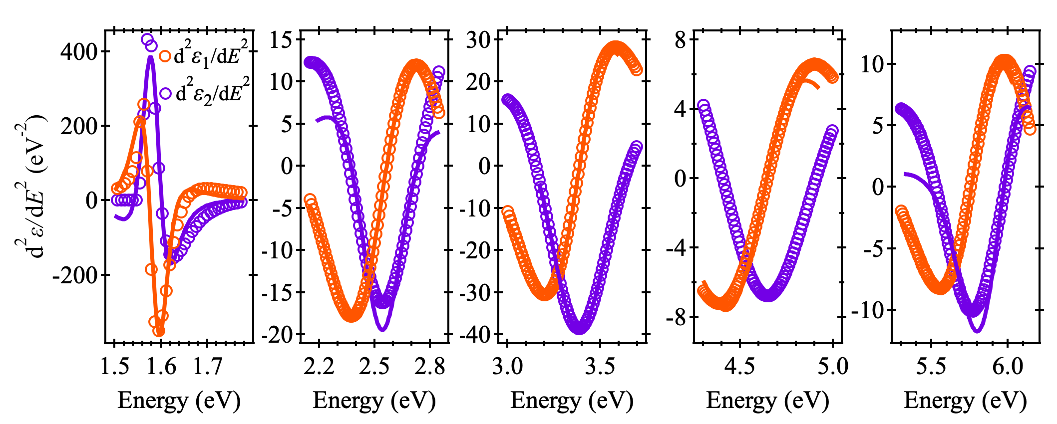
The transition energies obtained from this analysis are eV, eV, eV, eV eV. We could not extract an energy associated with the transition at the high energy limit of the dispersion, since it is not fully captured by the measurement range.
The three transitions , and are commonly identified 41, 8, 37, however, and are not often observed or remarked on. Our obtained value for the bandgap is similar to those previously determined 46, 41, 11, 10, which has been attributed to a direct transition at the R symmetry point of the Brillouin zone 40, 10. Shirayama et al. reported the analysis of SE measurements over a wide spectral range, where several weak transitions are observed at high energies 10. In their work, critical points are identified at 2.53 and 3.24 eV in the dielectric function for MAPbI3 and are assigned to the direct optical transitions at the M and X points in the pseudocubic Brillouin zone, respectively. Leguy et al. also performed SE measurements up to photon energies up to 5.5 eV and fitted the data to determine critical-point energies of 1.62, 2.55, 3.31, 4.55, and 10 eV for single crystals of MAPbI3 but slightly different values of 1.61, 2.5, 2.85, 3.38, and 6.97 eV for thin films.40 In the study, the authors use quasi-particle self-consistent GW (QS-GW) calculations to derive optical constants up to photon energies of 10 eV, which are in good agreement with experimental data within in the spectral range of the measurements. In the calculated extinction coefficient spectrum, peaks are also predicted at 5.5 and 6.7 eV, which are not captured in their ellipsometry experiments, but are relatively close to the transitions observed in our experiments here.40 Hirasawa and co-workers also observed the transition at 4.8 eV in the absorption spectrum at a temperature of 4.2 K 60. Ndione and colleagues observed the transitions at 4.6 and 5.8 eV in the dielectric constant from SE measurements, but only included the transition at 4.6 eV in the critical-point analysis.45 Demchenko et al. performed SE measurements on MAPbI3 and extracted a dielectric constant that closely matches our obtained function, including the high energy features, likely originating from point transitions 44. Analysis of their band structure calculations showed that time-dependent hybrid functional calculations based on exchange-tuned HSE (TD-HSE), with spin-orbit coupling included in the calculation best reproduced the experimental data. Guerra and colleagues also observed the transitions at 4.6 and 5.8 eV via SE but did not measure spectrophotometry data beyond 5 eV. 46 In all the above studies, the highest energy optical transition is not investigated via spectrophotometry measurements in addition to SE.
2.1 Conclusions
In conclusion, we have used spectroscopic ellipsometry (SE) and spectrophotometry to identify optical transitions in MAPbI3 thin films and have determined the optical constants over a wide spectral range. We have shown how the SE data can be fitted with a Tauc-Lorentz dispersion model with six oscillators, using parameters that can be physically justified. These analyses are critical for constructing optical models for use in designing structures such as tandem solar cells. We have used critical-point analysis to show transitions at 1.58, 2.49, 3.36, 4.63 and 5.88 eV from the SE data, which is in excellent agreement with results from spectrophotometry. The transitions at 4.63 and 5.88 eV are not usually investigated due to experimental limitations and provide important information relating to the band structure of MAPbI3 and the potential applications of the material. Their origin remains unclear and further theoretical work should be carried out to understand the nature of these transitions and assist in accurately determining the fundamental physical characteristics of metal halide perovskites.
3 Experimental
3.1 Sample Preparation
Glass substrates were cleaned by sonicating in Helmanex III solution with dionized water, and subsequently sonicating in isopropyl alcohol. They are then treated with oxygen plasma for 10 minutes before being transferred to an inert environment for deposition. For the MAPbI3 precursor solution, a mixed solvent system was used with DMF and dimethylsulfoxide (DMSO). PbI2 and MAI were combined with a molar ratio of 1:1 in a DMF:DMSO ( 9:1) solvent at a concentration of 1M to form a PbI2-DMSO complex. The MAPbI3 solution was dispensed on the glass substrate and spin coated at 3000 RPM and after the the procedure is initiated, a flow of nitrogen gas is applied to the film to dry the parent solvent and produce smooth films. The MAPbI3 films are then annealed for 10 mins at 100 °C in a nitrogen atmosphere. For spectrophotometry measurements, a quartz substrate is used instead of glass and the precursor concentration of 0.5M is used instead to achieve a film thickness of 110 nm.
3.2 Sample Characterization
The samples were characterized using a Rigaku SmartLab X-ray diffractometer with a Cu K-alpha 9 kW anode. The scanning electron microscopy (SEM) was carried out using a Zeiss (LEO) 1450VP Scanning Electron Microscope with an accelerating voltage of 20 kV. The atomic-force microscopy (AFM) was performed with a Nanonics Imaging Hydra BioAFM system.
3.3 Spectroscopic Ellipsometry
A J.A. Woolam M-2000 spectroscopic ellipsometer was used to measure the induced polarization change in the MAPbI3 thin films for incident angles of 65 °, 70 °and 75 °. The samples were packaged in an inert environment and measured immediately after opening to ambient conditions. CompleteEase (J.A. Woolam) software is then used for the data analysis and dispersion model fitting, as described in the main text. The root mean squared error is calculated using the equation:
| (5) |
where is the number of wavelengths, is the number of fitting parameters and . The subscripts and denote the experimental data and the modeled data, respectively.
3.4 Spectrophotometry
A JASCO V-570 UV/Vis/NIR spectrophotometer was used to measure the optical transmission and specular reflectance of MAPbI3 thin films deposited on quartz. The data was used to provide an estimate for the absorption coefficient using the relation
| (6) |
where is the film thickness, is the transmission and is the reflectance.
The authors thank the Engineering and Physical Sciences Research Council (EPSRC) for funding the research.
References
- NREL 2019 NREL, NREL Efficiency Chart. 2019; \urlhttps://www.nrel.gov/pv/cell-efficiency.html
- Correa-Baena et al. 2017 Correa-Baena, J. P.; Saliba, M.; Buonassisi, T.; Grätzel, M.; Abate, A.; Tress, W.; Hagfeldt, A. Science 2017, 358, 739–744
- Sha et al. 2015 Sha, W. E.; Ren, X.; Chen, L.; Choy, W. C. Applied Physics Letters 2015, 106, 221104
- Polman et al. 2016 Polman, A.; Knight, M.; Garnett, E. C.; Ehrler, B.; Sinke, W. C. Science 2016, 352, aad4424–aad4424
- Braly et al. 2018 Braly, I. L.; Dequilettes, D. W.; Pazos-Outón, L. M.; Burke, S.; Ziffer, M. E.; Ginger, D. S.; Hillhouse, H. W. Nature Photonics 2018, 12, 355–361
- Paetzold et al. 2017 Paetzold, U. W. W.; Jaysankar, M.; Gehlhaar, R.; Ahlswede, E.; Paetel, S.; Qiu, W.; Bastos, J. P.; Rakocevic, L.; Richards, B. S.; Aernouts, T.; Powalla, M.; Poortmans, J. J. Mater. Chem. A 2017, 5, 9897–9906
- Albrecht et al. 2016 Albrecht, S.; Saliba, M.; Correa Baena, J. P.; Lang, F.; Kegelmann, L.; Mews, M.; Steier, L.; Abate, A.; Rappich, J.; Korte, L.; Schlatmann, R.; Nazeeruddin, M. K.; Hagfeldt, A.; Grätzel, M.; Rech, B. Energy Environ. Sci. 2016, 9, 81–88
- Jiang et al. 2016 Jiang, Y.; Almansouri, I.; Huang, S.; Young, T.; Li, Y.; Peng, Y.; Hou, Q.; Spiccia, L.; Bach, U.; Cheng, Y.-B.; Green, M.; Ho-Baillie, A. J. Mater. Chem. C 2016, 4, 5679–5689
- Mantilla-Perez et al. 2017 Mantilla-Perez, P.; Feurer, T.; Correa-Baena, J. P.; Liu, Q.; Colodrero, S.; Toudert, J.; Saliba, M.; Buecheler, S.; Hagfeldt, A.; Tiwari, A. N.; Martorell, J. ACS Photonics 2017, 4, 861–867
- Shirayama et al. 2016 Shirayama, M.; Kadowaki, H.; Miyadera, T.; Sugita, T.; Tamakoshi, M.; Kato, M.; Fujiseki, T.; Murata, D.; Hara, S.; Murakami, T. N.; Fujimoto, S.; Chikamatsu, M.; Fujiwara, H. Physical Review Applied 2016, 5, 014012
- De Wolf et al. 2014 De Wolf, S.; Holovsky, J.; Moon, S. J.; Löper, P.; Niesen, B.; Ledinsky, M.; Haug, F. J.; Yum, J. H.; Ballif, C. Journal of Physical Chemistry Letters 2014, 5, 1035–1039
- Xing et al. 2013 Xing, G.; Mathews, N.; Sun, S.; Lim, S. S.; Lam, Y. M.; Grätzel, M.; Mhaisalkar, S.; Sum, T. C. Science 2013, 342, 344 LP – 347
- Sun et al. 2014 Sun, S.; Salim, T.; Mathews, N.; Duchamp, M.; Boothroyd, C.; Xing, G.; Sum, T. C.; Lam, Y. M. Energy & Environmental Science 2014, 7, 399
- Miyata et al. 2015 Miyata, A.; Mitioglu, A.; Plochocka, P.; Portugall, O.; Wang, J. T.-W.; Stranks, S. D.; Snaith, H. J.; Nicholas, R. J. Nature Physics 2015, 11, 582–587
- Even et al. 2014 Even, J.; Pedesseau, L.; Katan, C. Journal of Physical Chemistry C 2014, 118, 11566–11572
- Yang et al. 2015 Yang, Y.; Yang, M.; Li, Z.; Crisp, R.; Zhu, K.; Beard, M. C. Journal of Physical Chemistry Letters 2015, 6, 4688–4692
- Piana et al. 2019 Piana, G. M.; Bailey, C. G.; Lagoudakis, P. G. The Journal of Physical Chemistry C 2019, 37, acs.jpcc.9b06712
- Giorgi et al. 2013 Giorgi, G.; Fujisawa, J. I.; Segawa, H.; Yamashita, K. Journal of Physical Chemistry Letters 2013, 4, 4213–4216
- Ziffer et al. 2016 Ziffer, M. E.; Mohammed, J. C.; Ginger, D. S. ACS Photonics 2016, 3, 1060–1068
- Li et al. 2018 Li, Z.; Moon, J.; Gharajeh, A.; Haroldson, R.; Hawkins, R.; Hu, W.; Zakhidov, A.; Gu, Q. ACS Nano 2018, 12, 10968–10976
- Wang et al. 2018 Wang, S.; Liu, Y.; Li, G.; Zhang, J.; Zhang, N.; Xiao, S.; Song, Q. Advanced Optical Materials 2018, 6, 1701266
- Wang et al. 2016 Wang, K.; Sun, W.; Li, J.; Gu, Z.; Xiao, S.; Song, Q. ACS Photonics 2016, 3, 1125–1130
- Stylianakis et al. 2019 Stylianakis, M. M.; Maksudov, T.; Panagiotopoulos, A.; Kakavelakis, G.; Petridis, K. Materials 2019, 16, 1–28
- Liao et al. 2015 Liao, Q.; Hu, K.; Zhang, H.; Wang, X.; Yao, J.; Fu, H. Advanced Materials 2015, 27, 3405–3410
- Zhu et al. 2015 Zhu, H.; Fu, Y.; Meng, F.; Wu, X.; Gong, Z.; Ding, Q.; Gustafsson, M. V.; Trinh, M. T.; Jin, S.; Zhu, X. Y. Nature Materials 2015, 14, 636–642
- Tan et al. 2014 Tan, Z. K.; Moghaddam, R. S.; Lai, M. L.; Docampo, P.; Higler, R.; Deschler, F.; Price, M.; Sadhanala, A.; Pazos, L. M.; Credgington, D.; Hanusch, F.; Bein, T.; Snaith, H. J.; Friend, R. H. Nature Nanotechnology 2014, 9, 687–692
- Cho et al. 2015 Cho, H.; Jeong, S. H.; Park, M. H.; Kim, Y. H.; Wolf, C.; Lee, C. L.; Heo, J. H.; Sadhanala, A.; Myoung, N. S.; Yoo, S.; Im, S. H.; Friend, R. H.; Lee, T. W. Science 2015, 350, 1222–1225
- Ling et al. 2016 Ling, Y.; Yuan, Z.; Tian, Y.; Wang, X.; Wang, J. C.; Xin, Y.; Hanson, K.; Ma, B.; Gao, H. Advanced Materials 2016, 28, 305–311
- Liang et al. 2016 Liang, J.; Zhang, Y.; Guo, X.; Gan, Z.; Lin, J.; Fan, Y.; Liu, X. RSC Advances 2016, 6, 71070–71075
- Saidaminov et al. 2015 Saidaminov, M. I.; Adinolfi, V.; Comin, R.; Abdelhady, A. L.; Peng, W.; Dursun, I.; Yuan, M.; Hoogland, S.; Sargent, E. H.; Bakr, O. M. Nature Communications 2015, 6, 8724
- Fang et al. 2015 Fang, Y.; Dong, Q.; Shao, Y.; Yuan, Y.; Huang, J. Nature Photonics 2015, 9, 679–686
- Bao et al. 2017 Bao, C.; Chen, Z.; Fang, Y.; Wei, H.; Deng, Y.; Xiao, X.; Li, L.; Huang, J. Advanced Materials 2017, 29, 1703209
- Ball et al. 2015 Ball, J. M.; Stranks, S. D.; Hörantner, M. T.; Hüttner, S.; Zhang, W.; Crossland, E. J.; Ramirez, I.; Riede, M.; Johnston, M. B.; Friend, R. H.; Snaith, H. J. Energy and Environmental Science 2015, 8, 602–609
- Ziang et al. 2015 Ziang, X.; Shifeng, L.; Laixiang, Q.; Shuping, P.; Wei, W.; Yu, Y.; Li, Y.; Zhijian, C.; Shufeng, W.; Honglin, D.; Minghui, Y.; Qin, G. G. Optical Materials Express 2015, 5, 29
- Jiang et al. 2015 Jiang, Y.; Green, M. A.; Sheng, R.; Ho-Baillie, A. Solar Energy Materials and Solar Cells 2015, 137, 253–257
- Marronnier et al. 2018 Marronnier, A.; Lee, H.; Lee, H.; Kim, M.; Eypert, C.; Gaston, J. P.; Roma, G.; Tondelier, D.; Geffroy, B.; Bonnassieux, Y. Solar Energy Materials and Solar Cells 2018, 178, 179–185
- Wang et al. 2019 Wang, X.; Gong, J.; Shan, X.; Zhang, M.; Xu, Z.; Dai, R.; Wang, Z.; Wang, S.; Fang, X.; Zhang, Z. Journal of Physical Chemistry C 2019, 123, 1362–1369
- Lin et al. 2015 Lin, Q.; Armin, A.; Nagiri, R. C. R.; Burn, P. L.; Meredith, P. Nature Photonics 2015, 9, 106–112
- Leguy et al. 2015 Leguy, A. M.; Hu, Y.; Campoy-Quiles, M.; Alonso, M. I.; Weber, O. J.; Azarhoosh, P.; Van Schilfgaarde, M.; Weller, M. T.; Bein, T.; Nelson, J.; Docampo, P.; Barnes, P. R. Chemistry of Materials 2015, 27, 3397–3407
- Leguy et al. 2016 Leguy, A. M.; Azarhoosh, P.; Alonso, M. I.; Campoy-Quiles, M.; Weber, O. J.; Yao, J.; Bryant, D.; Weller, M. T.; Nelson, J.; Walsh, A.; Van Schilfgaarde, M.; Barnes, P. R. Nanoscale 2016, 8, 6317–6327
- Löper et al. 2015 Löper, P.; Stuckelberger, M.; Niesen, B.; Werner, J.; Filipič, M.; Moon, S. J.; Yum, J. H.; Topič, M.; De Wolf, S.; Ballif, C. Journal of Physical Chemistry Letters 2015, 6, 66–71
- Jiang et al. 2016 Jiang, Y.; Soufiani, A. M.; Gentle, A.; Huang, F.; Ho-Baillie, A.; Green, M. A. Applied Physics Letters 2016, 108, 61905
- van Eerden et al. 2017 van Eerden, M.; Jaysankar, M.; Hadipour, A.; Merckx, T.; Schermer, J. J.; Aernouts, T.; Poortmans, J.; Paetzold, U. W. Advanced Optical Materials 2017, 5, 1700151
- Demchenko et al. 2016 Demchenko, D. O.; Izyumskaya, N.; Feneberg, M.; Avrutin, V.; Özgür,; Goldhahn, R.; Morkoç, H. Physical Review B 2016, 94, 75206
- Ndione et al. 2016 Ndione, P. F.; Li, Z.; Zhu, K. Journal of Materials Chemistry C 2016, 4, 7775–7782
- Guerra et al. 2017 Guerra, J. A.; Tejada, A.; Korte, L.; Kegelmann, L.; Töfflinger, J. A.; Albrecht, S.; Rech, B.; Weingärtner, R. Journal of Applied Physics 2017, 121, 173104
- Brittman and Garnett 2016 Brittman, S.; Garnett, E. C. Journal of Physical Chemistry C 2016, 120, 616–620
- Chen et al. 2019 Chen, X.; Wang, Y.; Song, J.; Li, X.; Xu, J.; Zeng, H.; Sun, H. Journal of Physical Chemistry C 2019, 123, 10564–10570
- Shirai 2017 Shirai, H. Ellipsometry - Principles and Techniques for Materials Characterization; 2017
- Zhao et al. 2018 Zhao, M.; Shi, Y.; Dai, J.; Lian, J. Journal of Materials Chemistry C 2018, 6, 10450–10455
- Alias et al. 2016 Alias, M. S.; Dursun, I.; Saidaminov, M. I.; Diallo, E. M.; Mishra, P.; Ng, T. K.; Bakr, O. M.; Ooi, B. S. Optics Express 2016, 24, 16586
- Werner et al. 2018 Werner, J.; Nogay, G.; Sahli, F.; Yang, T. C. J.; Bräuninger, M.; Christmann, G.; Walter, A.; Kamino, B. A.; Fiala, P.; Löper, P.; Nicolay, S.; Jeangros, Q.; Niesen, B.; Ballif, C. ACS Energy Letters 2018, 3, 742–747
- Whitcher et al. 2018 Whitcher, T. J.; Zhu, J. X.; Chi, X.; Hu, H.; Zhao, D.; Asmara, T. C.; Yu, X.; Breese, M. B.; Castro Neto, A. H.; Lam, Y. M.; Wee, A. T.; Chia, E. E.; Rusydi, A. Physical Review X 2018, 8
- Conings et al. 2016 Conings, B.; Babayigit, A.; Klug, M. T.; Bai, S.; Gauquelin, N.; Sakai, N.; Wang, J. T.-W.; Verbeeck, J.; Boyen, H.-G.; Snaith, H. J. Advanced Materials 2016, 1–9
- Jeon et al. 2014 Jeon, N. J.; Noh, J. H.; Kim, Y. C.; Yang, W. S.; Ryu, S.; Seok, S. I. Nature materials 2014, 13, 1–7
- Xia et al. 2016 Xia, B.; Wu, Z.; Dong, H.; Xi, J.; Wu, W.; Lei, T.; Xi, K.; Yuan, F.; Jiao, B.; Xiao, L.; Gong, Q.; Hou, X. Journal of Materials Chemistry A 2016, 4, 6295–6303
- Gao et al. 2018 Gao, Y.; Yang, L.; Wang, F.; Sui, Y.; Sun, Y.; Wei, M.; Cao, J.; Liu, H. Superlattices and Microstructures 2018, 113, 761–768
- Jellison and Modine 1996 Jellison, G. E.; Modine, F. A. Applied Physics Letters 1996, 69, 371–373
- Fujiwara et al. 2018 Fujiwara, H.; Kato, M.; Tamakoshi, M.; Miyadera, T.; Chikamatsu, M. Physica Status Solidi (A) Applications and Materials Science 2018, 215
- Hirasawa et al. 1994 Hirasawa, M.; Ishihara, T.; Goto, T. Journal of the Physical Society of Japan 1994, 63, 3870–3879