Mobility enhancement in graphene by in situ reduction of random strain fluctuations
Abstract
Microscopic corrugations are ubiquitous in graphene even when placed on atomically flat substrates. These result in random local strain fluctuations limiting the carrier mobility of high quality hBN-supported graphene devices. We present transport measurements in hBN-encapsulated devices where such strain fluctuations can be in situ reduced by increasing the average uniaxial strain. When of uniaxial strain is applied to the graphene, an enhancement of the carrier mobility by is observed while the residual doping reduces by . We demonstrate a strong correlation between the mobility and the residual doping, from which we conclude that random local strain fluctuations are the dominant source of disorder limiting the mobility in these devices. Our findings are also supported by Raman spectroscopy measurements.
In the first generation of graphene devices, where was used as the substrate, it is commonly believed that random charged impurities at the substrate surface are the dominant source of disorder limiting the device quality Ando (2006); Nomura and MacDonald (2007); Hwang et al. (2007); Adam et al. (2007); Chen et al. (2008a, b); Hong et al. (2009). One way to improve the device quality is to suspend graphene to spatially separate it from the charge traps Bolotin et al. (2008a); Du et al. (2008); Bolotin et al. (2008b); Tombros et al. (2011); Maurand et al. (2014). Nowadays, a more widely used technique is to place graphene on hexagonal boron nitride (hBN) Dean et al. (2010); Zomer et al. (2011); Mayorov et al. (2011); Wang et al. (2013), which is atomically flat and expected to be free of surface charge traps. A significant improvement in device quality has been achieved, exhibiting very high carrier mobilities, enabling the observation of a series of new physical phenomena, such as the fractional quantum Hall effect Bolotin et al. (2009); Du et al. (2009); Dean et al. (2011), transverse magnetic focusing Taychatanapat et al. (2013); Lee et al. (2016); Chen et al. (2016) and various moiré superlattice effects Ponomarenko et al. (2013); Dean et al. (2013); Hunt et al. (2013); Wang et al. (2019a). Although the mobility of hBN-supported graphene devices is generally higher than that of the -supported, the reported mobility values vary over a large range, suggesting another mechanism that limits the mobility. It has been pointed out that random strain fluctuations (RSFs) in graphene could be a dominant source of disorder leading to electron scattering Katsnelson and Geim (2008). In a recent statistical study of many devices on hBN substrates, a clear correlation between the carrier mobility and the residual doping was found, pointing to RSFs as the dominant microscopic source of scattering Couto et al. (2014). The residual doping caused by charge fluctuations manifests in a broadening of the resistance peak around the charge neutrality point (CNP). Similar results have been found as well in bilayer graphene Engels et al. (2014).
Ripples and pronounced corrugations can form naturally in graphene due to its two-dimensional nature, as, for example, demonstrated by transmission electron microscopy in suspended graphene membranes Meyer et al. (2007). In stacked layers, microscopic corrugations can spontaneously form during exfoliation due to thermal fluctuations at room temperature Abedpour et al. (2007); Fasolino et al. (2007); Katsnelson and Geim (2008). These corrugations might persist through the fabrication processes and give rise to RSFs in the final device. In -supported devices, nanometer-scale ripples have been observed in scanning probe microscopy studies Ishigami et al. (2007); Stolyarova et al. (2007); Geringer et al. (2009); Cullen et al. (2010) and their effects on electron transport have been reported in weak localization studies Morozov et al. (2006); Tikhonenko et al. (2008); Lundeberg and Folk (2010). Although the hBN surface is typically much flatter, height fluctuations are still present in hBN-supported graphene devices Dean et al. (2010), which can result in RSFs. These RSFs have been confirmed in Raman spectroscopy measurements Neumann et al. (2015); Banszerus et al. (2017).
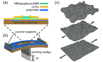
Here we demonstrate in a direct experiment that RSFs can be the mechanism limiting the mobility of encapsulated devices. We compare the transport characteristics of individual devices before and after increasing the average uniaxial strain, which directly reduces the strain fluctuations in the same device. In Fig. 1(c) the RSFs in graphene lattice are illustrated, which we believe can be reduced gradually by increasing the average strain, as indicated by the arrows. The reduction of the RSFs due to increasing average strain is further confirmed by directly probing the RSFs using Raman spectroscopy Neumann et al. (2015). This not only allows us to determine the dominant microscopic mechanism, but also to actually increase the mobility of the device.
The setup of the experiment is shown schematically in Fig. 1(a,b). It allows us to tune the average uniaxial strain in hBN-encapsulated graphene devices by bending a flexible substrate Wang et al. (2019b). The displacement of the pushing-wedge relative to the mounting position determines the deformation of the substrate and is used to tune the average strain in the graphene. The devices are fabricated using a dry-transfer method Wang et al. (2013), where we pick up a thick hBN as the top layer, then an exfoliated monolayer graphene flake from natural graphite and a thick hBN as the bottom layer. The assembled stack is then deposited onto a metallic gate structure prefabricated on a polyimide-coated phosphor bronze plate. Edge contacts Wang et al. (2013) (Cr/Au, /) are made with a controlled etching recipe, which stops in the middle of the bottom hBN, with the remaining hBN acting as the insulating layer between the contacts and the bottom gate Wang et al. (2019b), see Fig. 1(a).
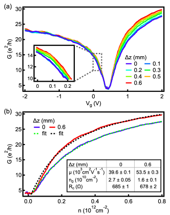
To investigate the effects of average strain on the transport characteristics of graphene, we measure the two-terminal differential conductance as a function of the gate voltage for different values, as plotted in Fig. 2(a). The measurements were performed at low temperature () using standard low-frequency lock-in techniques. The CNP is at , indicating an offset p-doping in our device. The conductance of the graphene increases faster when gated away from the CNP for larger , suggesting an increase in field effect mobility with increasing . This effect is reversible when is decreased (see Supplementary Material). A displacement of corresponds to of average strain, which is determined from Raman measurements shown later Wang et al. (2019b). The conductance starts to saturate at higher gate voltages because of the contact resistance. On the hole side (p-doping), a p-n junction forms near each contact due to the n-doping from the contact, resulting in a sightly larger contact resistance and a lower saturation conductance, which renders the mobility-change less visible. The zoomed-in data in the inset of Fig. 2(a) shows qualitatively the same effect as for the electron side.
To quantitatively evaluate the effects of strain tuning on the electrical properties of graphene, we fit each curve on the electron side (n-doping) with the following formula based on the Drude model Hong et al. (2009); Dean et al. (2010):
| (1) |
where is the elementary charge and is the geometry factor describing the aspect ratio, which is 1.28 in this case (see Supplementary Material). The fitting parameters are the charge-carrier density independent mobility , the residual doping around the CNP and the contact resistance . The charge-carrier density is calculated from the applied gate voltage with a lever arm of using a parallel plate capacitor model. The thickness of the bottom hBN, which is the gate dielectric, is determined by atomic force microscopy. Two examples of the fitting are shown as dashed lines for = 0 and in Fig. 2(b) with the corresponding parameters given in the inset.
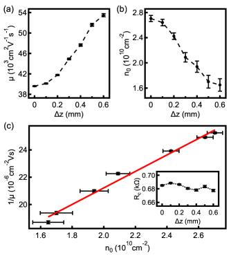
The fitting results for and are plotted as a function of in Fig. 3(a,b), respectively. The mobility shows a clear increase with increasing , while decreases significantly. The change is slower in the beginning, which might be attributed to a small mechanical hysteresis of the bending setup. The extracted contact resistance (including line resistance) is shown in the inset of Fig. 3(c) and is essentially unaffected by the bending, demonstrating the mechanical robustness of the device for these levels of applied average strain Wang et al. (2019b). The mobility increases from to when is increased from 0 to . At the same time the residual doping drops gradually from () to (). The (, ) pairs are plotted as versus in Fig. 3(c), clearly demonstrating the proportionality between and . The same analysis is performed for the hole side and similar results are obtained with a larger contact resistance (see Supplementary Material), which is consistent with the interpretation that the p-n junction makes the effect less pronounced on the hole side.
Since the graphene is encapsulated with hBN, it is very unlikely that the small applied average strain changes the charged impurities at the graphene-hBN interfaces, ruling them out as dominant mechanism for the observed mobility increase. An artificial effect due to the change of the gate capacitance with strain is also ruled out Wang et al. (2019b), because the CNP appears at the same gate voltage for all values.
RSFs have been identified theoretically as a possible source of disorder limiting charge carrier mobility Katsnelson and Geim (2008). Strong evidence of this mechanism has been found in a statistical study involving many devices, where a clear linear relation between and was observed, with Couto et al. (2014). Moreover, a detailed microscopic mechanism was proposed in which the variation of was attributed to RSFs-induced scalar potentials, while the limitation in was attributed to randomly varying pseudomagnetic fields Couto et al. (2014). Fitting our data linearly in Fig. 3(c) yields and . It shows a similar slope (), allowing us to draw two conclusions. First, the charge carrier mobility is limited by RSFs and second, the control of the average strain allows us to control the RSFs and hence the mobility. The offset might imply another mobility limiting mechanism when RSFs are not dominating anymore. The value nearly coincides with the mobility of the devices, in which no mobility enhancement due to increasing average strain is observed (discussed later).
Theoretically both, in-plane and out-of-plane, strain fluctuations can contribute to this effect Couto et al. (2014). In a previous study of weak localization on -supported graphene devices Lundeberg and Folk (2010), a reduction of the phase coherence time was found for an increasing in-plane magnetic field. It has been attributed to an enhanced dephasing rate due to a random vector potential generated by the in-plane magnetic field penetrating out-of-plane corrugations in the graphene layer. Similar effects have been observed in encapsulated devices Zihlmann et al. (2018, ), strongly suggesting that out-of-plane corrugations are also present in encapsulated graphene. We therefore attribute the mobility increase in our experiment to the reducing of out-of-plane strain fluctuations, as illustrated in Fig. 1(c).
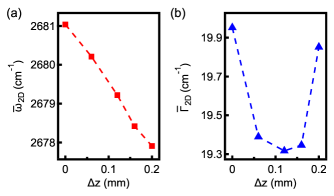
To further substantiate our findings, we use spatially resolved Raman spectroscopy to directly probe the RSFs at room temperature. For small uniaxial strain, which is the case in our experiment, the graphene Raman 2D peak can be fitted by a single Lorentzian Mohiuddin et al. (2009), with a center frequency and linewidth . The center frequency redshifts with increasing strain, while the linewidth broadens due to the splitting of the 2D peak Mohr et al. (2009); Huang et al. (2010). It has been shown that nanometer-scale strain inhomogeneities within the laser spot () also broadens the 2D peak Neumann et al. (2015), originating from averaging over regions with different local strain and hence different . Therefore, can be used to probe the RSFs. We perform spatially resolved Raman spectroscopy and extract maps of and for different . The mean value of the center frequency averaged over the whole device is plotted as a function of in Fig. 4(a). It shifts linearly to lower values with increasing , indicating an increasing average strain in the graphene sheet Mohiuddin et al. (2009). The shift at corresponds to an externally induced average strain of Wang et al. (2019b). In Fig. 4(b) the averaged value of the 2D peak linewidth is plotted as a function of , showing nonmonotonic characteristics with a minimum of at . It first decreases with increasing before increasing again, which can be explained by the competition between the two broadening mechanisms. The initial value of () is larger than the intrinsic linewidth () of the 2D peak Neumann et al. (2015), indicating that RSFs are present in our graphene. We attribute the decrease of to a reduction of the RSFs due to the externally applied strain, as illustrated in Fig. 1(c). When the broadening of the 2D peak induced by the increasing average strain dominates, increases again with increasing .
Our interpretation is also consistent with weak localization measurements we performed to extract characteristic scattering times (see Supplementary Material). We find that the intervalley scattering time is much longer than the elastic scattering time (determined from the mobility), implying that the mobility is not limited by intervalley scattering processes (scattering on short-range potentials, e.g. defects, edges). In contrast, the intravalley scattering time (the time needed to break the effective single-valley time-reversal symmetry) is nearly identical to , pointing to RSFs-induced random pseudomagnetic fields as the main factors limiting the mobility Couto et al. (2014). For charged impurities, it has been argued that Couto et al. (2014), which is not the case here.
We have observed a clear increase in the mobility with increasing average strain in more than 5 devices with their mobility values varying from to . In Fig. 3(a), there is also an indication that the mobility starts to saturate when it approaches higher values. For the devices with a mobility larger than , the mobility-increase effect is absent. (Examples are presented in the Supplementary Material). These observations suggest that either the RSFs cannot be fully reduced by increasing the average strain or another mechanism is at play for ultra high mobility devices.
In conclusion, we have demonstrated an in situ reduction of the random RSFs in individual encapsulated graphene devices by increasing the average strain. In low-temperature transport measurements, an enhancement of the carrier mobility by is observed while the residual doping reduces by when of average strain is applied to the graphene. The linear correlation between and reveals that random RSFs are the dominant scattering mechanism. These findings are further substantiated by Raman spectroscopy, in which the 2D peak linewidth , first decreases with increasing average strain before the average strain induced broadening dominates. The in situ straining allows us to directly compare results on individual devices and to avoid statistics over different devices. Using this technique we have directly confirmed that random RSFs are the dominant scattering mechanism limiting the mobility in most hBN-supported graphene devices. For devices with even higher mobilities, either the reduction of RSFs is not possible, or another scattering mechanism becomes dominant.
.1 Author contributions
L.W. fabricated the devices, performed the measurements and did the data analysis. P.M. helped to understand the data. P.M., S.Z. and A.B. helped with the data analysis. P.M., S.Z. and D.I. supported the device fabrication. K.W. and T.T. provided high-quality hBN. C.S. initiated and supervised the project. L.W. wrote the paper and all authors discussed the results and worked on the manuscript. All data in this publication are available in numerical form at: https://doi.org/10.5281/zenodo.3464530.
Acknowledgments
This work has received funding from the Swiss Nanoscience Institute (SNI), the ERC project TopSupra (787414), the European Union Horizon 2020 research and innovation programme under grant agreement No. 785219 (Graphene Flagship), the Swiss National Science Foundation, the Swiss NCCR QSIT, Topograph, ISpinText FlagERA network and from the OTKA FK-123894 grants. P.M. acknowledges support from the Bolyai Fellowship, the Marie Curie grant and the National Research, Development and Innovation Fund of Hungary within the Quantum Technology National Excellence Program (Project No. 2017-1.2.1-NKP-2017-00001). K.W. and T.T. acknowledge support from the Elemental Strategy Initiative conducted by the MEXT, Japan and the CREST (JPMJCR15F3), JST. The authors thank Francisco Guinea and Peter Rickhaus for fruitful discussions, and Sascha Martin and his team for their technical support.
References
- Ando (2006) T. Ando, J. Phys. Soc. Jpn. 75, 074716 (2006).
- Nomura and MacDonald (2007) K. Nomura and A. H. MacDonald, Phys. Rev. Lett. 98, 076602 (2007).
- Hwang et al. (2007) E. H. Hwang, S. Adam, and S. Das Sarma, Phys. Rev. Lett. 98, 186806 (2007).
- Adam et al. (2007) S. Adam, E. H. Hwang, V. M. Galitski, and S. DasSarma, Proc. Natl. Acad. Sci. U.S.A. 104, 18392 (2007).
- Chen et al. (2008a) J.-H. Chen, C. Jang, S. Adam, M. S. Fuhrer, E. D. Williams, and M. Ishigami, Nature Physics 4, 377 (2008a).
- Chen et al. (2008b) J.-H. Chen, C. Jang, S. Xiao, M. Ishigami, and M. S. Fuhrer, Nature Nanotechnology 3, 206 (2008b).
- Hong et al. (2009) X. Hong, K. Zou, and J. Zhu, Phys. Rev. B 80, 241415 (2009).
- Bolotin et al. (2008a) K. Bolotin, K. Sikes, Z. Jiang, M. Klima, G. Fudenberg, J. Hone, P. Kim, and H. Stormer, Solid State Communications 146, 351 (2008a).
- Du et al. (2008) X. Du, I. Skachko, A. Barker, and E. Y. Andrei, Nature Nanotechnology 3, 491 (2008).
- Bolotin et al. (2008b) K. I. Bolotin, K. J. Sikes, J. Hone, H. L. Stormer, and P. Kim, Phys. Rev. Lett. 101, 096802 (2008b).
- Tombros et al. (2011) N. Tombros, A. Veligura, J. Junesch, J. Jasper van den Berg, P. J. Zomer, M. Wojtaszek, I. J. Vera Marun, H. T. Jonkman, and B. J. van Wees, Journal of Applied Physics 109, 093702 (2011).
- Maurand et al. (2014) R. Maurand, P. Rickhaus, P. Makk, S. Hess, E. Tóvári, C. Handschin, M. Weiss, and C. Schönenberger, Carbon 79, 486 (2014).
- Dean et al. (2010) C. R. Dean, A. F. Young, I. Meric, C. Lee, L. Wang, S. Sorgenfrei, K. Watanabe, T. Taniguchi, P. Kim, K. L. Shepard, and J. Hone, Nature Nanotechnology 5, 722 (2010).
- Zomer et al. (2011) P. J. Zomer, S. P. Dash, N. Tombros, and B. J. van Wees, Applied Physics Letters 99, 232104 (2011).
- Mayorov et al. (2011) A. S. Mayorov, R. V. Gorbachev, S. V. Morozov, L. Britnell, R. Jalil, L. A. Ponomarenko, P. Blake, K. S. Novoselov, K. Watanabe, T. Taniguchi, and A. K. Geim, Nano Lett. 11, 2396 (2011).
- Wang et al. (2013) L. Wang, I. Meric, P. Y. Huang, Q. Gao, Y. Gao, H. Tran, T. Taniguchi, K. Watanabe, L. M. Campos, D. A. Muller, J. Guo, P. Kim, J. Hone, K. L. Shepard, and C. R. Dean, Science 342, 614 (2013).
- Bolotin et al. (2009) K. I. Bolotin, F. Ghahari, M. D. Shulman, H. L. Stormer, and P. Kim, Nature 462, 196 (2009).
- Du et al. (2009) X. Du, I. Skachko, F. Duerr, A. Luican, and E. Y. Andrei, Nature 462, 192 (2009).
- Dean et al. (2011) C. R. Dean, A. F. Young, P. Cadden-Zimansky, L. Wang, H. Ren, K. Watanabe, T. Taniguchi, P. Kim, J. Hone, and K. L. Shepard, Nature Physics 7, 693 (2011).
- Taychatanapat et al. (2013) T. Taychatanapat, K. Watanabe, T. Taniguchi, and P. Jarillo-Herrero, Nature Physics 9, 225 (2013).
- Lee et al. (2016) M. Lee, J. R. Wallbank, P. Gallagher, K. Watanabe, T. Taniguchi, V. I. Fal’ko, and D. Goldhaber-Gordon, Science 353, 1526 (2016).
- Chen et al. (2016) S. Chen, Z. Han, M. M. Elahi, K. M. M. Habib, L. Wang, B. Wen, Y. Gao, T. Taniguchi, K. Watanabe, J. Hone, A. W. Ghosh, and C. R. Dean, Science 353, 1522 (2016).
- Ponomarenko et al. (2013) L. A. Ponomarenko, R. V. Gorbachev, G. L. Yu, D. C. Elias, R. Jalil, A. A. Patel, A. Mishchenko, A. S. Mayorov, C. R. Woods, J. R. Wallbank, M. Mucha-Kruczynski, B. A. Piot, M. Potemski, I. V. Grigorieva, K. S. Novoselov, F. Guinea, V. I. Fal’ko, and A. K. Geim, Nature 497, 594 (2013).
- Dean et al. (2013) C. R. Dean, L. Wang, P. Maher, C. Forsythe, F. Ghahari, Y. Gao, J. Katoch, M. Ishigami, P. Moon, M. Koshino, T. Taniguchi, K. Watanabe, K. L. Shepard, J. Hone, and P. Kim, Nature 497, 598 (2013).
- Hunt et al. (2013) B. Hunt, J. D. Sanchez-Yamagishi, A. F. Young, M. Yankowitz, B. J. LeRoy, K. Watanabe, T. Taniguchi, P. Moon, M. Koshino, P. Jarillo-Herrero, and R. C. Ashoori, Science 340, 1427 (2013).
- Wang et al. (2019a) L. Wang, S. Zihlmann, M.-H. Liu, P. Makk, K. Watanabe, T. Taniguchi, A. Baumgartner, and C. Schönenberger, Nano Lett. 19, 2371 (2019a).
- Katsnelson and Geim (2008) M. Katsnelson and A. Geim, Phil. Trans. R. Soc. A 366, 195 (2008).
- Couto et al. (2014) N. J. G. Couto, D. Costanzo, S. Engels, D.-K. Ki, K. Watanabe, T. Taniguchi, C. Stampfer, F. Guinea, and A. F. Morpurgo, Phys. Rev. X 4, 041019 (2014).
- Engels et al. (2014) S. Engels, B. Terrés, A. Epping, T. Khodkov, K. Watanabe, T. Taniguchi, B. Beschoten, and C. Stampfer, Phys. Rev. Lett. 113, 126801 (2014).
- Meyer et al. (2007) J. C. Meyer, A. K. Geim, M. I. Katsnelson, K. S. Novoselov, T. J. Booth, and S. Roth, Nature 446, 60 (2007).
- Abedpour et al. (2007) N. Abedpour, M. Neek-Amal, R. Asgari, F. Shahbazi, N. Nafari, and M. R. R. Tabar, Phys. Rev. B 76, 195407 (2007).
- Fasolino et al. (2007) A. Fasolino, J. H. Los, and M. I. Katsnelson, Nature Materials 6, 858 (2007).
- Ishigami et al. (2007) M. Ishigami, J. H. Chen, W. G. Cullen, M. S. Fuhrer, and E. D. Williams, Nano Lett. 7, 1643 (2007).
- Stolyarova et al. (2007) E. Stolyarova, K. T. Rim, S. Ryu, J. Maultzsch, P. Kim, L. E. Brus, T. F. Heinz, M. S. Hybertsen, and G. W. Flynn, Proc. Natl. Acad. Sci. U.S.A. 104, 9209 (2007).
- Geringer et al. (2009) V. Geringer, M. Liebmann, T. Echtermeyer, S. Runte, M. Schmidt, R. Rückamp, M. C. Lemme, and M. Morgenstern, Phys. Rev. Lett. 102, 076102 (2009).
- Cullen et al. (2010) W. G. Cullen, M. Yamamoto, K. M. Burson, J. H. Chen, C. Jang, L. Li, M. S. Fuhrer, and E. D. Williams, Phys. Rev. Lett. 105, 215504 (2010).
- Morozov et al. (2006) S. V. Morozov, K. S. Novoselov, M. I. Katsnelson, F. Schedin, L. A. Ponomarenko, D. Jiang, and A. K. Geim, Phys. Rev. Lett. 97, 016801 (2006).
- Tikhonenko et al. (2008) F. V. Tikhonenko, D. W. Horsell, R. V. Gorbachev, and A. K. Savchenko, Phys. Rev. Lett. 100, 056802 (2008).
- Lundeberg and Folk (2010) M. B. Lundeberg and J. A. Folk, Phys. Rev. Lett. 105, 146804 (2010).
- Neumann et al. (2015) C. Neumann, S. Reichardt, P. Venezuela, M. Drögeler, L. Banszerus, M. Schmitz, K. Watanabe, T. Taniguchi, F. Mauri, B. Beschoten, S. V. Rotkin, and C. Stampfer, Nature Communications 6, 8429 (2015).
- Banszerus et al. (2017) L. Banszerus, H. Janssen, M. Otto, A. Epping, T. Taniguchi, K. Watanabe, B. Beschoten, D. Neumaier, and C. Stampfer, 2D Materials 4, 025030 (2017).
- Wang et al. (2019b) L. Wang, S. Zihlmann, A. Baumgartner, J. Overbeck, K. Watanabe, T. Taniguchi, P. Makk, and C. Schönenberger, Nano Lett. 19, 4097 (2019b).
- Zihlmann et al. (2018) S. Zihlmann, A. W. Cummings, J. H. Garcia, M. Kedves, K. Watanabe, T. Taniguchi, C. Schönenberger, and P. Makk, Phys. Rev. B 97, 075434 (2018).
- (44) S. Zihlmann, P. Makk, M. K. Rehmann, L. Wang, M. Kedves, D. I. Indolese, K. Watanabe, T. Taniguchi, D. M. Zumbühl, and C. Schönenberger, in preparation .
- Mohiuddin et al. (2009) T. M. G. Mohiuddin, A. Lombardo, R. R. Nair, A. Bonetti, G. Savini, R. Jalil, N. Bonini, D. M. Basko, C. Galiotis, N. Marzari, K. S. Novoselov, A. K. Geim, and A. C. Ferrari, Phys. Rev. B 79, 205433 (2009).
- Mohr et al. (2009) M. Mohr, K. Papagelis, J. Maultzsch, and C. Thomsen, Phys. Rev. B 80, 205410 (2009).
- Huang et al. (2010) M. Huang, H. Yan, T. F. Heinz, and J. Hone, Nano Lett. 10, 4074 (2010).