The valley Nernst effect in WSe2
The Hall effect can be extended by inducing a temperature gradient in lieu of electric field that is known as the Nernst (-Ettingshausen) effect. The recently discovered spin Nernst effect in heavy metals continues to enrich the picture of Nernst effect-related phenomena. However, the collection would not be complete without mentioning the valley degree of freedom benchmarked by the observation of the valley Hall effect. Here we show the experimental evidence of its missing counterpart, the valley Nernst effect. Using millimeter-sized WSe2 mono-multi-layers and the ferromagnetic resonance-spin pumping technique, we are able to apply a temperature gradient by off-centering the sample in the radio frequency cavity and address a single valley through spin-valley coupling. The combination of a temperature gradient and the valley polarization leads to the valley Nernst effect in WSe2 that we detect electrically at room temperature. The valley Nernst coefficient is in very good agreement with the predicted value.
Recently, there has been tremendous interest in layered transition metal dichalcogenides (TMDCs). It started with the discovery that the canonical TMDC MoS2 becomes a direct bandgap semiconductor when isolated in monolayer form Splendiani2010 ; Mak2010 . Many of the TMDCs have since been shown to exhibit a strong excitonic feature, showing strong and spectrally narrow photoluminescence and absorption making them very good candidates for novel optoelectronic devices Lopez-Sanchez2013 ; Gutierrez2013 . The combination of a bandgap (1-2 eV) and an atomically thin conducting channel also makes TMDCs ideal materials for next generation field effect transitors in microelectronics Radisavljevic2011 . Finally, in the monolayer form, due to the breaking of inversion symmetry and strong spin-orbit coupling, the carriers in TMDCs carry a valley index noted or . This valley degree of freedom refers to local extrema in the band structure of TMDC monolayers at the points of the two-dimensional Brillouin zone and it can be exploited to develop novel valleytronic devices Xiao2012 ; Zeng2012 ; Mak2012 . In MX2 (M=Mo, W and X=S, Se) monolayers, the broken inversion symmetry and strong spin-orbit coupling originating from the -orbitals of the transition metal atom align the electron spins near opposite valleys and to opposite out-of-plane directions thus preserving time reversal symmetry. The broken spatial inversion symmetry also generates large Berry curvatures (BC) near the valleys, the BC being opposite at opposite valleys Xiao2010 . This effect gives rise to unconventional electronic properties such as the valley Hall effect Mak2014 ; Xiao2012 . An interesting growing field of investigation consists in coupling the valley physics with thermoelectrics. Several valley-dependent thermoelectric effects have already been predicted theoretically in monolayer TMDCs such as the spin Nernst effect (SNE, thermoelectric counterpart of the spin Hall effect Sinova2015 ; Meyer2017 ; Sheng2017 ) and the valley Nernst effect (VNE) Yu2015 ; Sharma2018 . Hence, the experimental demonstration of those effects could give rise to a new field called valley caloritronics (by analogy with spin caloritronics Bauer2012 ) with the advantage that the coupled valley-spin degree of freedom is more robust than the spin with respect to external magnetic fields due to the large intrinsic spin-orbit coupling. One main obstacle to the observation of the VNE comes from the absence of large area TMDC monolayers which is a prerequisite to apply macroscopic temperature gradients. Here we use the van der Waals epitaxy to grow high-quality WSe2 mono- and multi-layer on epitaxial graphene on SiC over 1 cm2 Koma1992 ; Dau2018 . By this, we are able to apply temperature gradients in WSe2 on mm scale. However, in order to detect electrically the VNE, one needs to lift the - valley degeneracy, i.e. breaking time reversal symmetry and creating a population imbalance between the two valleys. To do so, we use the ferromagnetic resonance-spin pumping (FMR-SP) technique Ando2011 ; Rojas-Sanchez2013 ; Oyarzun2016 ; Hou2016 by growing in-situ the Al/NiFe/Al magnetic stack on top of the WSe2 layer. By suitably adjusting the position of the sample into the cavity, at the FMR of NiFe, we are able to: (i) generate a temperature gradient along the sample and (ii) address a single valley by spin pumping when the magnetic field is applied perpendicular to the film. Eventually, we detect the VNE which is in quantitative agreement with theoretical predictions.
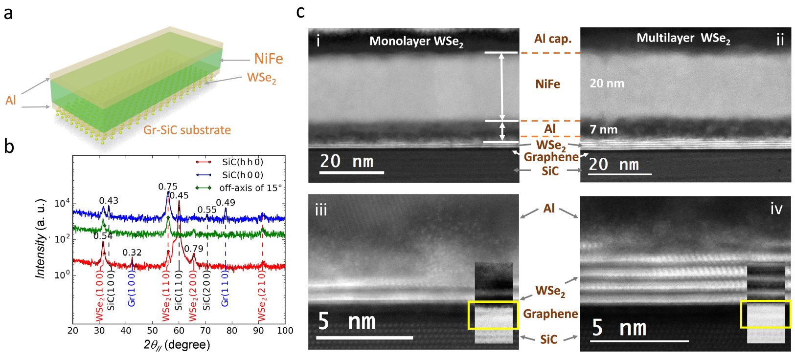
The growth of mono- and multi-layer of WSe2 is performed under ultrahigh vacuum by molecular beam epitaxy (MBE) in the van der Waals regime on epitaxial graphene on SiC. The graphene layer was grown by chemical vapor deposition on the Si face of SiC. The VNE is expected to be very large and dominant at the top of the valence band at the and points of the 2D Brillouin zone. Hence WSe2 layers are p doped by introducing 0.1 % of Nb in order to shift the Fermi level to the top of the valence band Pandey2018 . In Fig. 1b, ex-situ grazing incidence x-ray diffraction shows the single crystalline character of the WSe2 layers and the measured lattice parameter which is the one of bulk WSe2. More characterization results on the WSe2 layers are given in the Supplementary Material. We demonstrate that the Nb incorporation does not affect the growth and crystallinity of the WSe2 layers but it makes them conducting at room temperature which provides electronic states for carrier diffusion and the detection of the VNE (see Supplementary Material). WSe2 films are finally capped with a thin 10 nm-thick amorphous Se layer to allow air-transfer to another deposition chamber to grow the Al(7 nm)/NiFe(20 nm)/Al(5 nm) stacking after thermal desorption of amorphous Se.
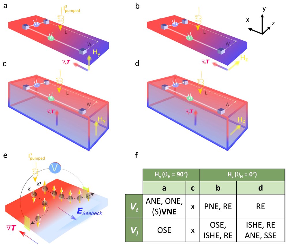
Figure 1c shows the cross-sectional scanning transmission electron microscopy (STEM) micrographs with high-angle annular dark-field imaging (HAADF) technique of the stacks made of monolayer (Fig. 1c(i) and 1c(iii) and multilayer (Fig. 1c(ii) and 1c(iv)) WSe2 used for the VNE experiments. The interfaces (graphene/WSe2) and (WSe2/metallic stack) with high crystalline quality are atomically resolved and abrupt. The number of WSe2 layers can be unambiguously determined based on the STEM images, and is in agreement with the estimation done by the combination of atomic force microscopy measurements and quartz crystal microbalance. We clearly note that the upper most layer WSe2 is degraded after Al deposition on top which is likely due to an intermixing of Al and Se. For that reason, in order to preserve the desired number of layers, especially in the case of one monolayer WSe2, we have systematically deposited at least 30 % of matter (Se,W,Nb) more.
Figure 2 illustrates the temperature-gradient induced voltages that are at play under the application of an external magnetic field coupled with spin injection via FMR-spin pumping. We also include rectification effets (RE) due to the anisotropic magnetoresistance and anomalous Hall effect in NiFe. They do not contribute to the measured voltage when the magnetic field and the magnetization are perpendicular to the film (i.e. = 90∘ and 270∘) Iguchi2017 ; Rojas-Sanchez2013 . It is shown that the VNE might be detected in the configuration where the magnetic field is perpendicular to the sample surface. We discuss below how we can electrically detect the VNE thanks to the FMR-SP technique and disqualify the spurious effects with robust arguments.
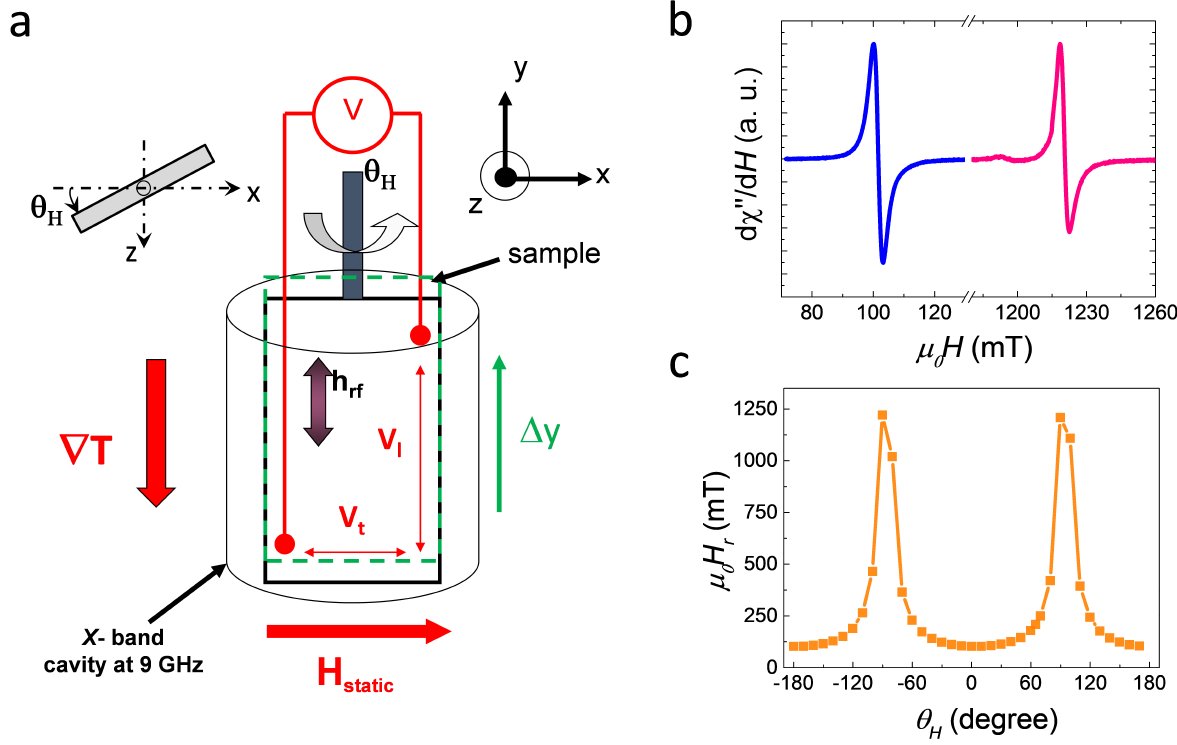
In order to study the VNE, the samples are cut into small 0.42.4 mm2 pieces, electrically contacted with Al wires using a mechanical bonding machine and finally introduced into the 9 GHz electron paramagnetic resonance cavity (Fig. 3a). The radio frequency (RF) power is set to 200 mW. In FMR-SP experiments, thermoelectric effects like the Seebeck effect are considered as parasitic effects and are usually removed from electrical signals Shiomi2014 . Here, we purposely position the sample away from the center of the cavity in order to generate a temperature gradient along the sample and study the VNE as shown in Fig. 3a. By shifting up (resp. down) the sample by , microwaves are more absorbed by the NiFe layer at the bottom (resp. top) of the sample with respect to the top (resp. bottom) leading to a temperature gradient along (resp. ). We measure simultaneously the FMR signal of the NiFe layer (Fig. 3b and 3c) and the voltage = + as a function of the angle from 0∘ to 360∘. The DC magnetic field Hstatic has a fixed direction along . (resp. ) corresponds to the longitudinal (resp. transverse) component of the voltage. When rotating the sample, we find that the magnetization of the soft NiFe layer is parallel to the applied field at = 90∘ and 270∘ at the ferromagnetic resonance by using a simple macrospin model and by minimizing the system energy Rojas-Sanchez2013 . We confirmed this prediction by out-of-plane anisotropic magnetoresistance measurements (see Supplementary Material).
Both voltage components contain a symmetric (s) and asymmetric (a) part with respect to the static magnetic field Hstatic defined as: = and = . is the voltage due to the Seebeck effect as a consequence of the off-centered position of the sample in the cavity and the resulting vertical temperature gradient. corresponds to the inverse spin Hall effect (ISHE) in the parallel configuration ( = 0∘ and 180∘) while corresponds to the ordinary Nernst effect (ONE), anomalous Nernst effect (ANE), SNE and VNE in the perpendicular configuration ( = 90∘ and 270∘)(see table in Fig. 2f). Due to time reversal symmetry, SNE and VNE are expected to give zero signal. However, in the perpendicular configuration, spin pumping allows to address a single spin/valley population leading to a net transverse voltage as illustrated in Fig. 2e.
We performed the measurements at room temperature for 4 different samples: 2 samples with one monolayer of WSe2 (samples A and B), a reference sample without WSe2 (sample C) and one sample with WSe2 multilayers (sample D). We first focus on sample A and detect a symmetric voltage in Fig. 4a demonstrating the large Seebeck effect in WSe2. The rotating sample disturbs the RF cavity settings and modifies the Q factor (proportional to the RF field ). Here, the Q factor and the Seebeck effect are minimum in the parallel configuration. The Seebeck voltage () varies between 10 and 35 V with a value of 22.6 V in the perpendicular geometry. If we assume that, at best, 1/10 of the Nb atoms are activated at room temperature, the expected doping level is 1011 cm-2 giving a Seebeck coefficient = 500 V/K Ghosh2015 ; Kim2010 . The temperature difference between the two electrical contacts () then ranges between 20 mK and 70 mK depending on the sample orientation. In the perpendicular configuration, the temperature difference is approximately 40 mK. is reported in Fig. 4c as a function of the applied field for two different angles = 0∘ (parallel configuration) and = 90∘ (perpendicular configuration), being the resonance field. In Fig. 4b, we show the full angular dependence of for . We clearly see that the signal is maximum in the perpendicular configuration.
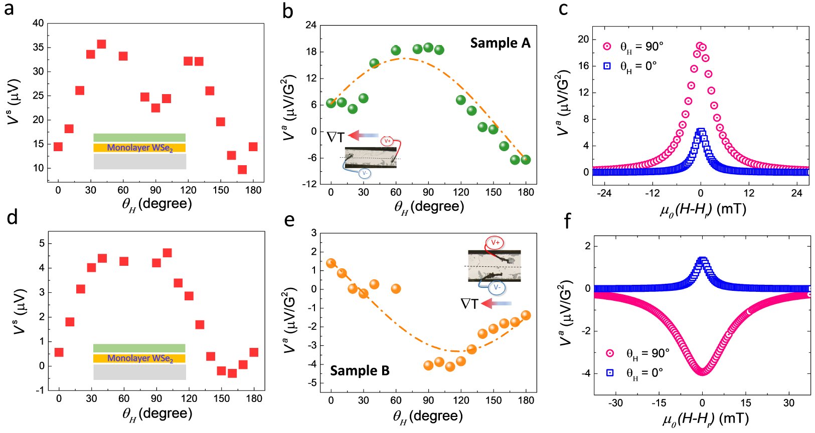
In Fig. 4e, we repeated the same measurements on sample B with the contacts at different positions and found the same behavior but with different signal amplitudes. Moreover, in sample B, is negative at = 90∘ since we reversed the polarity of the contacts ( and ) with respect to sample A as shown in the insets of Fig. 4b and 4e. As a comparison, in the reference sample C exhibits very low values in the whole angular range demonstrating that the Seebeck effect is negligible in the Al/NiFe/Al/graphene/SiC stack (see Supplementary Material). Furthermore, the full angular dependence of the measured voltage in sample C (Fig. 5a) shows two things: (i) zero voltage in the perpendicular configuration, indicating that the ONE in the full stack as well as the ANE in NiFe are negligible and not detectable. We also note that the ANE in NiFe (sample A) can be estimated as follows: 0.1 nV with in NiFe being of the order of 9 nV/K Miao2013 , = 70 mK and W 0.2 mm, L 1.3 mm being the transverse and longitudinal distances between the electrical contacts. The ANE voltage is indeed negligibly small compared with the measured in the perpendicular configuration; (ii) a cosine dependence corresponding well to the ISHE. We do not discuss here about the origin of this ISHE signal which probably comes from the self-conversion into the NiFe layer.
We then interpret the angular dependence of in samples A and B as the combination of the ISHE proportional to the in-plane component of the spin s// and the VNE proportional to the out-of-plane component of the spin s⟂. We can express the experimental data as: where for (s⟂ = 0) and for = 90∘ (s// = 0) in Fig. 4b and 4e. Here we do not consider the ONE in WSe2 since it is expected to be at least 3 orders of magnitude smaller than the VNE coefficient as discussed in Ref.Sharma2018 . Morever, if there exists a longitudinal temperature gradient as described in Fig. 2d, the contribution of the ANE and SSE in NiFe for the in-plane component can also be ignored as demonstrated in NiFe with FMR-SP experiment Noel2019 . We find ( = 6.4 V/G2, = 18.9 V/G2) for sample A and ( = 1.2 V/G2, = -4.1 V/G2) for sample B. The VNE coefficient is given by: = = where is the WSe2 transverse resistance between the two electrical contacts. This resistance is measured independently by transferring the same WSe2 film grown on mica onto a SiO2/Si substrate pre-patterned with a transfer length measurement (TLM) arrangement (see Supplementary Material). We find the VNE coefficient 38.9 pA/K for sample A and 38.8 pA/K for sample B. If we define where is the electron charge, the Planck constant and the Boltzmann constant, we obtain for 1 monolayer of WSe2.
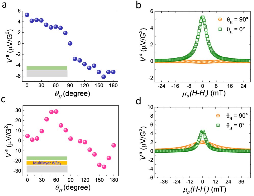
In the following, we assume that Nb doping shifts the Fermi level close to the top of the and valence bands. We also assume that the intervalley scattering time is longer than the characteristic momentum scattering time in the WSe2 layers. The VNE thus generates a pure transverse valley/spin current. The VNE coefficient vanishes when and bands are equally populated by time reversal symmetry. If we assume that FMR-SP in the perpendicular configuration allows to populate only the valley (100% valley polarization), the maximum expected value for the VNE coefficient is 0.09 at room temperature when the Fermi level is located between the , valence band edge Yu2015 . Experimentally, we find which is very close to the predicted maximum value. The experimental value suggests that the Fermi level lies approximately 0.11 eV above the top of the valence band Yu2015 . The Fermi energy corresponds to a hole density = 1.3 1011 cm-2 (where , , T, , denote valley degeneracy, effective hole mass, temperature, Boltzmann and reduced Planck constants, respectively), corroborating well with the hole doping range in our WSe2. Other features related to the VNE such as rf-power quadratic dependence and spatial-shift induced sign change of the voltage ( at = 90∘) are given in Supplementary Material. Our interpretation for the observation of VNE is also supported by the fact that we detect no voltage in the perpendicular configuration in the reference sample C (Fig. 5a and 5b). Moreover, we performed the same FMR-SP measurements on WSe2 multilayer as shown in Fig. 5c and 5d. In this case, the perpendicular voltage is much weaker than in the case of WSe2 monolayer and comparable to the in-plane signal. This is also true when we convert the voltages into currents by normalizing with the resistance measured in open-circuit condition: 0.18, 0.00 and 0.06 A/G2 for samples A, C and D, respectively. In particular, the maximum voltage is no longer located at = 90∘. This angular dependence of the voltage is still in qualitative agreement with the observation of the valley Nernst effect. Indeed, when increasing the number of layers, WSe2 becomes an indirect bandgap semiconductor with the top of the valence band at the point. As a consequence, when increasing the number of layers, we expect a sharp decrease of the valley Nernst effect in the valleys as observed experimentally. Second, the angular dependence of the transverse voltage of the monolayer, which shows a maximum when the spin of holes is pinned to the out-of-plane direction, results from the imbalance of the valley populations. Here, any signal arising from the Rashba spin-orbit coupling (induced by the asymmetric environment of WSe2 or induced by the proximity effect in graphene Yang2017 ) is neglected. In particular, the recently discussed spin-type Berry curvature Zhou2019 is orders of magnitude smaller than the intrinsic Berry curvature at the valence band edges of WSe2 monolayer. Finally, we note that the full angular dependence of the FMR-SP measurements in the case of WSe2 multilayers (Fig. 5c) needs further investigation in order to get insight into its behavior, in particular the appearance of the two maxima with opposite signs. We anticipate that the direct-to-indirect bandgap transition and Ising-Rashba spin-orbit effects Taguchi2018 associated with the restored inversion symmetry in the multilayer would be appropriate arguments to interpret the full angular dependence.
In conclusion, by applying a macroscopic temperature gradient and by addressing a single valley, we could demonstrate the large valley Nernst effect in monolayer WSe2. For this, we have grown high quality WSe2 monolayers on graphene by van der Waals epitaxy over large areas. At the ferromagnetic resonance of the NiFe film in contact with WSe2, we could both generate a temperature gradient in WSe2 at the millimeter scale and a valley polarization by spin pumping. This original technique allowed us to give an estimation of the valley Nernst coefficient that agrees well with the predicted value for one monolayer of WSe2. The Valley Nernst effect could be used as an alternative way to generate valley currents for valley-related physics.
Acknowlegments
The authors acknowledge the financial support from the ANR projects MoS2ValleyControl and MAGICVALLEY. The LANEF framework (No. ANR-10-LABX-51-01) is also acknowledged for its support with mutualized infrastructure. The authors thank A. Michon for his help in the preparation of Graphene/SiC subtrate, Y. Genuist for his help in the growth of metallic stacks, Nicolas Mollard for preparation of TEM samples and V. Mareau, L. Gonon for their assistance in Raman measurements.
Methods
Sample growth and characterization. The graphene/SiC substrate is first outgased at 750∘C during one hour in the MBE chamber with a base pressure in the low 10-10 mbar range. It is then kept at 500∘C during the co-deposition of W (0.01875 Å/s), Se (10-6 mbar) and Nb (0.01875 Å/s). W and Nb are evaporated thanks to e-gun evaporators and Se with a Knudsen cell. The Nb flux is pulsed in order to reach the right concentration of 0.1%. At the end of the growth, the whole film is annealed at 750∘C during 15 minutes under Se flux to improve the crystal quality Alvarez2018 . We obtain continuous and uniform WSe2 films on 55 mm2 graphene/SiC substrate.
X-ray diffraction analysis was performed with a SmartLab Rigaku diffractometer equipped with a Copper Rotating anode beam tube (Kα = 1.54 Å) and operated at 45 kV and 200 mA. A parabolic mirror and a parallel in-plane collimator of 0.5∘C of resolution was used in the primary optics and a second parallel collimator was used in the secondary side. A Kβ filter was used for all the measurements.
Raman measurements were done with a Horiba Raman set-up using a laser excitation source of 632 nm with spot size of 0.5 m. The signal was collected by choosing a 1800 grooves/mm grating.
WSe2 transfer. We adopted a wet transfer process that is described in details in Ref.Dau2019 for the transfer of WSe2 grown on mica onto SiO2/Si substrate.
Electrical contacts. The Ti/Pt contacts, which were pre-patterned on SiO2/Si substrate by lithography and etching followed by metal deposition, have thicknesses of 5 nm / 10 nm, respectively. See Supplemental Material for the distribution of the contact distance.
Contributions
M.T.D. performed the spin pumping measurements with the help of S.G. and V.M. M.T.D. and M.J. analysed and interpreted the spin pumping. C.V., C.B., M.T.D., T.G. and M.J. performed the transfer and electrical measurements. M.T.D. and C.V. grew the WSe2 layers and performed the Raman measurements. T.J. and B.H. performed the growth of graphene on SiC substrate. A.M. performed and analysed the X-ray diffraction data. B.G. performed the atomic force microscopy characterization. H.O. made the transmission electron microscopy observations. M.T.D. and M.J. wrote the paper with comments of all co-authors. M.J. initiated the study and supervised the project.
Competing interests
The authors declare no competing financial interests.
Data availability
The data that support the findings of this study are available from the corresponding author upon reasonable request.
References
- (1) Splendiani, A., Sun, L., Zhang, Y., Li, T., Kim, J., Chim, C. Y., Galli, G. & Wang, F. Emerging Photoluminescence in Monolayer MoS2. Nano Lett. 10, 1271 (2010).
- (2) Mak, K. F., Lee C., Hone J., Shan, J. & Heinz, T. F. Atomically thin MoS2: a new direct-gap semiconductor. Phys. Rev. Lett. 105, 136805 (2010).
- (3) Lopez-Sanchez, O., Lembke, D., Kayci, M., Radenovic, A. & Kis, A. Ultrasensitive photodetectors based on monolayer MoS2. Nat. Nanotechnol. 8, 497 (2013).
- (4) Gutiérrez, H. R., Perea-López, N., Elías, A. L., Berkdemir, A., Wang, B., Lv, R., López-Urías, F. L., Crespi, V. H., Terrones, H. & Terrones, M. Extraordinary room-temperature photoluminescence in triangular WS2 monolayers Nano Lett. 13, 3447 (2013).
- (5) Radisavljevic, B., Radenovic, A., Brivio, J., Giacometti, V. & Kis, A. Single-layer MoS2 transistors. Nat. Nanotechnol. 6, 147 (2011).
- (6) Xiao, D., Liu, G. B., Feng, W., Xu, X. & Yao, W. Coupled spin and valley physics in monolayers of MoS2 and other group-VI dichalcogenides. Phys. Rev. Lett. 108, 196802 (2012).
- (7) Zeng, H., Dai, J., Yao, W., Xiao, D. & Cui, X. Valley polarization in MoS2 monolayers by optical pumping Nat. Nanotechnol. 7, 490 (2012).
- (8) Mak, K. F., He, K., Shan, J. & Heinz, T. F. Control of valley polarization in monolayer MoS2 by optical helicity. Nat. Nanotechnol. 7, 494 (2012).
- (9) Xiao, D., Chang, M.-C. & Niu, Q. Berry phase effects on electronic properties. The valley Hall effect in MoS2 transistors. Rev. Mod. Phys. 82, 1959 (2010).
- (10) Mak, K. F., McGill, K. L., Park, J. & McEuen, P. L. Science 344, 1489 (2014).
- (11) Sinova, J., Valenzuela, S. O., Wunderlich, J., Back, C. H. & Jungwirth, T. Spin Hall effects. Rev. Mod. Phys. 87, 1213 (2015).
- (12) Meyer, S. et al. Observation of the spin Nernst effect. Nat. Mater., 16, 977 (2017).
- (13) Sheng, P., Sakuraba, Y., Lau, Y.-C., Takahashi, S., Mitani, S. & Hayashi, M. The spin Nernst effect in tungsten. Science Adv. 3, e1701503 (2017).
- (14) Yu, X.-Q., Zhu, Z.-G., Su, G. & Jauho, A.-P. Thermally driven pure spin and valley currents via the anomalous Nernst effect in monolayer group-VI dichalcogenides. Phys. Rev. Lett. 115, 246601 (2015).
- (15) Sharma, G. Tunable topological Nernst effect in two-dimensional transition-metal dichalcogenides. Phys. Rev. B 98, 075416 (2018).
- (16) Bauer, G. E. W., Saitoh, E. & Van Wees, B. J. Spin caloritronics. Nat. Mater. 11, 391 (2012).
- (17) Koma, A. Van der Waals epitaxy—a new epitaxial growth method for a highly lattice-mismatched system. Thin Solid Films 216, 72 (1992).
- (18) Dau, M. T. et al. Beyond van der Waals interaction: the case of MoSe2 epitaxially grown on few-layer graphene. ACS Nano 12, 2319 (2018).
- (19) Ando, K. et al. Inverse spin-Hall effect induced by spin pumping in metallic system. J. Appl. Phys. 109, 103913 (2011).
- (20) Rojas-Sanchez, J.-C. et al. Spin pumping and inverse spin Hall effect in germanium. Phys. Rev. B 88, 064403 (2013).
- (21) Oyarzun, S. et al. Evidence for spin-to-charge conversion by Rashba coupling in metallic states at the Fe/Ge(111) interface. Nat. Commun. 7, 13857 (2016).
- (22) Hou, D., Qiu, Zh., Iguchi, R., Sato, K., Vehstedt, E.K, Uchida, K., Bauer, G.E.W. & Saitoh, E. Observation of temperature-gradient-induced magnetization. Nat. Commun. 7, 12265 (2016).
- (23) Pandey, S. K., Alsalman, H., Azadani, J. G., Izquierdo, N., Low, T. & Campbell, S. A. Controlled p-type substitutional doping in large-area monolayer WSe2 crystals grown by chemical vapor deposition . Nanoscale 10, 21374 (2018).
- (24) Iguchi, R., & Saitoh, E. Measurement of spin pumping voltage separated from extrinsic microwave effects. J. Phys. Soc. Jpn. 86, 011003 (2017).
- (25) Shiomi, Y., Nomura, K., Kajiwara, Y., Eto, K., Novak, M., Segawa, K., Ando, Y. & Saitoh, E. Spin-electricity conversion induced by spin injection into topological insulators. Phys. Rev. Lett. 113, 196601 (2014).
- (26) Ghosh, K. & Singisetti, U. Thermoelectric transport coefficients in mono-layer MoS2 and WSe2: role of substrate, interface phonons, plasmon, and dynamic screening. J. Appl. Phys. 118, 135711 (2015).
- (27) Kim, J.-Y., Choi, S. M., Seo, W.-S. & Cho, W.-S. Thermal and electronic properties of exfoliated metal chalcogenides. Bull. Korean Chem. Soc. 31, 3225 (2010).
- (28) Miao, B. F., Huang, S. Y., Qu, D. & Chien, C. L. Inverse Spin Hall Effect in a Ferromagnetic Metal. Phys. Rev. Lett. 111, 066602 (2013).
- (29) Noel, P., Cosset-Cheneau, M., Haspot, V., Maurel, V., Lombard, Ch., Bibes, M., Barthelemy, A., Vila, L. & Attané, J.-P. Do thermal effects always contribute to spin pumping signals ?. https://arxiv.org/abs/1905.00771 (2019).
- (30) Yang, B., Lohmann, M., Barroso, D., Liao, I., Lin, Z., Liu, Y., Bartels, L., Watanabe, K., Taniguchi, T. & Shi, J. Strong electron-hole symmetric Rashba spin-orbit coupling in graphene/monolayer transition metal dichalcogenide heterostructures. Phys. Rev. B 96, 041409 (2017).
- (31) Zhou, B. T., Taguchi, K., Kawaguchi, Y., Tanaka, Y. & Law, K. T. Spin-orbit coupling induced valley Hall effects in transition-metal dichalcogenides. Commun. Phys. 2, 26 (2019).
- (32) Taguchi, K., Zhou, B. T., Kawaguchi, Y., Tanaka, Y. & Law, K. T. Valley Edelstein effect in monolayer transition-metal dichalcogenides. Phys. Rev. B 98, 035435 (2018).
- (33) Alvarez, C. J., Dau, M. T., Marty, A., Vergnaud, C., Le Poche, H., Pochet, P., Jamet, M. & Okuno, H. Impact of a van der Waals interface on intrinsic and extrinsic defects in an MoSe2 monolayer Nanotechnology 29, 425706 (2018).
- (34) Dau, M. T., Vergnaud, C., Gay, M., Alvarez, C. J., Marty, A., Beigné, C., Jalabert, D., Jacquot, J.-F., Renault, O., Okuno, H., and Jamet, M. Van der Waals epitaxy of Mn-doped MoSe2 on mica. APL Mater. 7, 051111 (2019).