Charge carrier density, mobility and Seebeck coefficient of melt-grown bulk ZnGa2O4 single crystals
Abstract
The temperature dependence of the charge carrier density, mobility and Seebeck coefficient of melt-grown, bulk ZnGa2O4 single crystals was measured between 10 K and 310 K. The electrical conductivity at room temperature is about S/cm due to a high electron concentration of cm-3, caused by unintenional doping. The mobility at room temperature is cm2/Vs, whereas the scattering on ionized impurities limits the mobility to cm2/Vs for temperatures lower than 180 K. The Seebeck coefficient relative to aluminum at room temperature is V/K and shows a temperature dependence as expected for degenerate semiconductors. At low temperatures, around 60 K we observed a maximum of the Seebeck coefficient due to the phonon drag effect.
Transparent conducting oxides (TCOs) have drawn attention due to their possible application in high power, optical or gas sensing devicesGrundmann et al. (2010); Lorenz et al. (2016); Fortunato, Barquinha, and Martins (2012); Higashiwaki et al. (2016); Suzuki et al. (2007); Green et al. (2016); Chabak et al. (2016); Galazka (2018). Recently, -Ga2O3 and related semiconducting oxides with ultra-wide bandgaps of over 4 eV are in the focus, since they offer transparency in the visible spectrum, semiconducting behaviour and breakthrough electric fields of several MV/cm. The fundamental research has been extended from binary to ternary and quaternary systems to find new substrate material for epitaxial thin film growth, as well as to make use of a higher degree of freedom in terms of dopingGalazka et al. (2019).
ZnGa2O4 is a novel ternary conducting oxide that crystallizes in the spinel crystal structure, which makes it interesting as a substrate for ferrite spinelsGalazka et al. (2019). Furthermore, the material might be promising for electric application, which gives rise to a study of the fundamental electric and thermoelectric transport properties. The isotropic thermal conductivity at room temperature is W/mKGalazka et al. (2019), but many other material parameters remain to be clarified. Theoretical values for the bandgap of ZnGa2O4 were predicted to be indirect (K-) with values between 2.69 eV - 4.71 eVZerarga et al. (2011); Pisani, Maitra, and Valentí (2006); López et al. (2009); Karazhanov and Ravindran (2010); Brik (2010); Dixit et al. (2011); Xia et al. (2018), or direct (-) with values of 2.79 eVSampath, Kanhere, and Pandey (1999). The experimental bandgap was found at the values of 4.0 eV – 5.0 eV measured on synthetized ZnO:Ga2O3 powdersSampath and Cordaro (2005), ceramicsOmata et al. (1994), films obtained by mist-CVDOshima et al. (2014), films obtained by sol-gelZhang et al. (2010) and on bulk crystals obtained by the flux methodYan, Takei, and Kawazoe (2005), while experimental optical bandgap measured on bulk single crystals obtained from the melt is 4.6 eVGalazka et al. (2019). Theoretical calculated effective masses are in the range of Sampath, Kanhere, and Pandey (1999); Karazhanov and Ravindran (2010); Dixit et al. (2011); Xia et al. (2018). Only little is known about electric transport parameters. On one hand, ZnGa2O4 ceramics show low electrical conductivity ( S/cm Omata et al. (1994)). On the other hand, melt-grown bulk single crystals showed high electrical conductivity of about 50 - 500 S/cmGalazka et al. (2019).
In this work, we investigate as-grown bulk ZnGa2O4 of blueish coloration
and perform temperature-dependent Seebeck-, van-der-Pauw- and Hall-measurements between K and K. We discuss the results in terms of electron scattering processes and thermoelectric effects observed in a degenerate semiconductor.
The samples have been grown using the vertical gradient freeze methodGalazka et al. (2019), without intentional doping. Powdered ZnO and Ga2O3, each with a purity of 99.999 % were used as starting materials. The growth was performed in an Ir crucible with an excess of 0.2 mol.% of ZnO to compensate its losses at high temperatures. The growth atmosphere consisted of O2/Ar (20 vol.% / 80 vol.%). The heating up and cooling down times were 7 and 10 hours, respectively, and resulted in single crystal blocks with blue and transparent appearance. As can be seen from ref. Galazka et al. (2019) Fig. 7, the composition of the obtained crystals were close to stoichiometric. All crystals grown in this way showed similar defect structure as has been reportedGalazka et al. (2019), without low-angle grain boundaries. For further details on the growth conditions, structural and chemical characterization of the material, see Galazka, et al.Galazka et al. (2019).
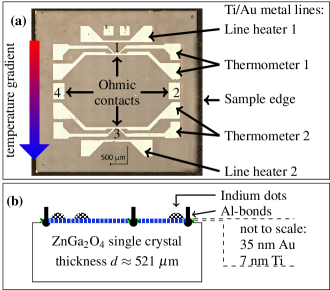
To perform electric and thermoelectric measurements, a microlab, consisting of metal lines, has been manufactured on the surface. Figure 1 shows a microscopic image and a schematic view of the microlab, which allows the measurement of the Seebeck coefficient, conductivity using the van-der-Pauw method, as well as the Hall resistance. The Ohmic contacts used for measuring the thermovoltage are located in the middle of the four-point metal lines (Ohmic contacts 1 and 3 in Fig. 1), which serve as thermometers and allow the measurement of the temperature difference .
The microlab has been manufactured by standard photolithography and magnetron sputtering of titanium (7 nm) and gold (35 nm), after cleaning with acetone and isopropanol and subsequent drying. The as-sputtered metal lines of the microlab are isolated due to a Schottky contact relative to the ZnGa2O4 bulk crystal. Ohmic contacts with the ZnGa2O4 bulk crystal were achieved by direct wedge bonding with an Al/Si-wire (99%/1%) on the deposited metal structure, creating point contacts. To keep some parts of the microlab isolated relative to the thin film, the electrical contacts were prepared by attaching gold wire with indium to the Ti/Au metal lines. This procedure can be compared to the one used with -Ga2O3, seeAhrling et al. (2019); Boy et al. (2019). Figure 2 displays exemplary two-point I-V curves at room temperature.
The experimental procedure is carried out in a flow cryostat between K and K. After the bath temperature is stabilized, the van-der-Pauw and Hall measurements are carried out. Subsequently the Seebeck measurements are performed. The Seebeck measurements involve the creation of various temperature differences by imprinting different currents into the line heater. The thermovoltage is measured simultaneously for approximately three minutes, which allows to create a stable temperature difference across the sample. Then, while keeping the heating current constant, the resistances of the thermometers are being measured. This procedure is repeated within bath temperature intervals of 10 K.
In the following, we present the measurement results of the electric and the thermoelectric transport, as shown in figs. 2-8.
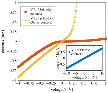
To quantify the quality of the contacts, two-point curves were measured at room temperature and are shown in Fig. 2. The red square and orange triangles in the main plot show the curves of Schottky-Schottky and Schottky-Ohmic contacts, respectively. The curve for the Ohmic-Ohmic contact configuration can be seen as blue circles in the inset. The two-point graphs of the different Schottky contact configurations show the expected diode curve for forward bias (positive voltages) as well as the reverse bias (negative voltages). The dynamic resistance of the Schottky-Ohmic and Schottky-Schottky contacts are at least two orders of magnitude higher than the Ohmic-Ohmic contact resistance of 12 shown in the inset. Therefore a good electrical isolation between the heater lines and the ZnGa2O4 bulk crystal is concluded.
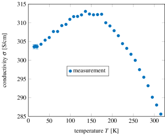
The temperature dependence of the electrical conductivity is shown in Fig. 3. The conductivity is between and S/cm for the entire temperature range. For higher temperatures K the conductivity is decreasing. A maximum can be identified around K.
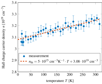
Hall measurements were performed to determine the charge carrier density, which is depicted as a function of temperature in Fig. 4. A linear fit has been added to the plot, showing the weak temperature dependence. The Hall charge carrier density is in the range of cm-3 for the entire temperature range.
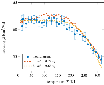
The measurement of the electrical conductivity and Hall charge carrier density allows the calculation of the electron mobility . The electron mobility as a function of temperature is plotted in Fig. 5. At room temperature a mobility of cm2/Vs was measured. The mobility increases with decreasing temperature, until it reaches a plateau-like feature of cm2/Vs at K and below.
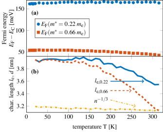
To understand the results of the mobility, we calculated the mean free path of the electrons as a function of temperature, shown in Fig. 6 b). The mean free path can be calculated with the following formula
| (1) |
Here, is the Fermi energy and is the elemental charge. The Fermi energy was computed from the reduced electron chemical potential with the Boltzmann constant . The reduced electron chemical potential was calculated after NilssonNilsson (1973). This method interpolates the range between non-degenerated and degenerated semiconductors and determines the reduced electron chemical potential as follows
| (2) |
| (3) |
with being the effective density of states in the conduction band,
| (4) |
with the Planck’s constant. For effective masses of and Fermi energies of meV and meV above the conduction band minimum were obtained, respectively. This can be seen in Fig. 6 a).
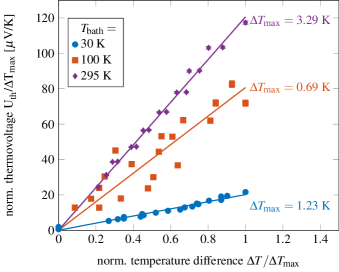
In order to determine the thermoelectric properties, the thermovoltage is measured as a function of temperature difference. Figure 7 shows the normalized thermovoltage as a function of normalized temperature difference for bath temperatures of 30 K, 100 K, and 295 K. Small offsets (V) have been substracted from the data. The Seebeck coefficient is determined by
| (5) |
The change of the Seebeck coefficient as a function of bath temperature can be observed by the change of slope of the linear fits. Furthermore the maximum achieved temperature difference is depicted in Fig. 7.
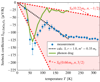
The Seebeck coefficient has been determined for temperatures between 30 K and 320 K. The results are shown in Fig. 8 as a function of temperature . The Seebeck coefficients are in the range of V/K at K to V/K at room temperature. Below room temperature, the magnitude of the Seebeck coefficient decreases steadily down to K. For lower temperatures it shows a maximum at K.
In the following, we discuss all electrical and thermoelectrical properties in detail.
The electrical conductivity shown in Fig. 3 has a weak temperature dependence when compared with -Ga2O3Ahrling et al. (2019). As can be seen, this originates partly from the very weak temperature dependence of the Hall charge carrier density shown in Fig. 4. The unintentionally doped ZnGa2O4 is a degenerate semiconductor, which we conclude from the high magnitude and the weak temperature dependence of the charge carrier density and the calculated relative Fermi-level shown in Fig. 6 a), which is above the lower conduction band edge for all cases. Furthermore, this is in agreement with the Mott-criterium, which gives an approximation for a critical charge carrier density above which the semiconductor is degenerate. is the vacuum permittivity and is the reduced Planck’s constant. For the static dielectric constant has been used, which was obtained for Zn0.99Cu0.01Ga2O4Lu et al. (2017). The critical charge carrier density is cm-3 and cm-3, depending on the assumed effective masses . The critical carrier density lies underneath the Hall charge carrier density for all cases.
The charge carrier mobility was calculated and shown in Fig. 5. For the high temperature regime, it is limited by optical phonon scattering (OP). OP scattering can deviate significantly from the dependence of acoustic deformation potential scatteringSeeger (2004) due to its inelastic nature.
In the chemically related TCOs Ma et al. (2016) and ZnOBikowski and Ellmer (2014) it was shown that polar optical phonon scattering is the dominant scattering mechanism at high temperatures due to the partial ionic bonding. The following model after Askerov has proved to be useful for the interpretation of polar optical phonon scattering in degenerate semiconductorsAskerov (1994); Bikowski and Ellmer (2014)
| (6) |
with
| (7) |
the average energy of the optical phonons, the polaron coupling constant and is the high frequency dielectric constant. The high frequency dielectric constant of Passlack et al. (1994); Rebien et al. (2002) () has been used since the exact value for is unknown and it is expected in the same range as the values for ZnOAshkenov et al. (2003); Decremps et al. (2002) ().
The mean free path in Fig. 6 b) shows, that there is a temperature independent process that limits the mean free path at nm. This limit becomes clear for temperatures lower than K when electron-phonon interaction becomes weaker. Furthermore, the mean free distance between single ionized donors, assuming a simple cubic distribution, is shown. One can see, that there is an upper limit of nm and that the simple model for the donor distribution predicts a mean distance in the same range.
There are two approaches to explain the low temperature limit of the electron mobility. On one hand, it can be explained by the scattering of electrons with neutral impurities. The Hall charge carrier data in Fig. 4 suggests a constant ionization of the donors, acceptors and vacancies for the investigated temperature interval, so This leads to the assumption, that also the neutral impurity density Electron scattering on neutral impurities can be described bySeeger (2004) . Thus, if there is no change in concentration of the neutral impurities, there will be a temperature independent upper limit of the mobility, which can be observed in Fig. 5.
On the other hand, high electron concentrations in semiconductors mean, that there is either a high concentration of singly ionized impurities, or a lower density of ionized impurities with a higher degree of ionization. Furthermore, the scattering of electrons in degenerate semiconductors with ionized impurities can be described by the Brooks-Hering equationBikowski and Ellmer (2014); Dingle (1955); Ellmer (2001)
| (8) |
with
| (9) |
is the degree of ionization and is the density of ionized impurities, with the donator and acceptor densities and , respectively. The ionized impurity scattering is expected to be more dominant, since there is a high density of ionized donors due to the high Hall charge carrier density.
The fits shown in Fig. 5 have been calculated using the Matthiessen’s rule and consider the scattering on polar optical phonons and ionized impurities after eq. (6) and eq. (8), respectively
| (10) |
for effective masses of and . The fit (red dashed line) results in an acceptor density cm-3 and a phonon energy of meV. For the fit (yellow dotted line) an acceptor density cm-3 and a phonon energy of meV were obtained. These results lead to compensation ratios () between and for and , respectively.
The measurement of the thermovoltage as a function of temperature difference, as shown in Fig. 7, reveals that there is a major change in the maximum reached temperature difference for different bath temperatures. This also correlates with the precision of the data points. The maximum reached temperature difference depends on the imprinted heating power, but is more strongly dependent on the thermal conductivity of the material. The higher the thermal conductivity of the material, the more difficult it is to create large temperature differences. This is the main reason for the increasing uncertainty of the Seebeck coefficient going to lower bath temperatures. From the change of maximum temperature difference, one can conclude the change of the thermal conductivity of the material. Having a look at the precision of the data in Fig. 8, which is correlated with the maximum temperature difference and therefore with the thermal conductivity, one can see, that the thermal conductivity seems to have a maximum around K and decreases as the temperature decreases further. This could be due to a distortion of the lattice, which has been reported in Galazka et al. (2019) as particles revealing Moiré patterns in transmission electron microscopy bright field images.
The Seebeck coefficient (Fig. 8) is negative, which means that electrons are the majority charge carriers. This is in agreement with the Hall charge carrier results. The Seebeck coefficient is lower than the one reportedBoy et al. (2019) for -Ga2O3 in the same temperature regime. This can be understood, since the semiconducting oxide investigated here is degenerate.
The red area in Fig. 8 marks calculated Seebeck coefficients following the commonly used equationSeeger (2004) for degenerate semiconductors assuming the effective mass to be between and and the scattering factor to be between and
| (11) |
The scattering parameter is based on the assumption, that the electron relaxation time follows a power law dependence . In other investigations it was observed, that and holds in the investigated temperature interval. In general and is calculated by the assumption and
| (12) |
A calculated Seebeck coefficient with and was added as a thin black dashed line, which fits the data for K K best. For K the difference of the calculated Seebeck coefficient with , and the measured Seebeck coefficient is plotted as a green solid line. We account the observed deviation of the theoretical Seebeck coefficient to be due to the phonon drag effect.
In conclusion, we have shown, that as-grown, bulk ZnGa2O4 single crystals show higher electrical conductivity at room temperature ( S/cm) than in earlier investigated ZnGa2O4 ceramics ( S/cm Omata et al. (1994)), as-grown Ga2O3 bulk ( S/cmAhrling et al. (2019)) or as-grown ZnO bulk ( S/cmXin-Hua et al. (2006)) due to the high charge carrier density. The donor mechanisms remain to be established. The wide band-gap of the material makes it suitable for application in high-power devices, which can become even more promising, if -doped material becomes available.
In terms of the power factor for thermoelectric applications, ZnGa2O4 has a room temperature value of W/K, being more than 5 times higher than that of Ga2O3 with W/K. Therefore, ZnGa2O4 is a more promising material for thermoelectric applications of transparent conducting oxides.
Acknowledgement
This work was performed in the framework of GraFOx, a Leibniz-ScienceCampus partially funded by the Leibniz association and by the German Science Foundation (DFG-FI932/10-1 and DFG-FI932/11-1).
References
- Grundmann et al. (2010) M. Grundmann, H. Frenzel, A. Lajn, M. Lorenz, F. Schein, and H. von Wenckstern, “Transparent semiconducting oxides: materials and devices,” physica status solidi (a) 207, 1437–1449 (2010).
- Lorenz et al. (2016) M. Lorenz, M. S. R. Rao, T. Venkatesan, E. Fortunato, P. Barquinha, R. Branquinho, D. Salgueiro, R. Martins, E. Carlos, A. Liu, F. K. Shan, M. Grundmann, H. Boschker, J. Mukherjee, M. Priyadarshini, N. DasGupta, D. J. Rogers, F. H. Teherani, E. V. Sandana, P. Bove, K. Rietwyk, A. Zaban, A. Veziridis, A. Weidenkaff, M. Muralidhar, M. Murakami, S. Abel, J. Fompeyrine, J. Zuniga-Perez, R. Ramesh, N. A. Spaldin, S. Ostanin, V. Borisov, I. Mertig, V. Lazenka, G. Srinivasan, W. Prellier, M. Uchida, M. Kawasaki, R. Pentcheva, P. Gegenwart, F. M. Granozio, J. Fontcuberta, and N. Pryds, “The 2016 oxide electronic materials and oxide interfaces roadmap,” Journal of Physics D: Applied Physics 49, 433001 (2016).
- Fortunato, Barquinha, and Martins (2012) E. Fortunato, P. Barquinha, and R. Martins, “Oxide semiconductor thin-film transistors: A review of recent advances,” Advanced Materials 24, 2945–2986 (2012).
- Higashiwaki et al. (2016) M. Higashiwaki, H. Murakami, Y. Kumagai, and A. Kuramata, “Current status of power devices,” Japanese Journal of Applied Physics 55, 1202A1 (2016).
- Suzuki et al. (2007) N. Suzuki, S. Ohira, M. Tanaka, T. Sugawara, K. Nakajima, and T. Shishido, “Fabrication and characterization of transparent conductive Sn-doped single crystal,” physica status solidi (c) 4, 2310–2313 (2007).
- Green et al. (2016) A. J. Green, K. D. Chabak, E. R. Heller, R. C. Fitch, M. Baldini, A. Fiedler, K. Irmscher, G. Wagner, Z. Galazka, S. E. Tetlak, A. Crespo, K. Leedy, and G. H. Jessen, “/cm breakdown strength of MOVPE-grown Sn-doped- mosfets,” IEEE Electron Device Letters 37, 902–905 (2016).
- Chabak et al. (2016) K. D. Chabak, N. Moser, A. J. Green, D. E. Walker, S. E. Tetlak, E. Heller, A. Crespo, R. Fitch, J. P. McCandless, K. Leedy, M. Baldini, G. Wagner, Z. Galazka, X. Li, and G. Jessen, “Enhancement-mode wrap-gate fin field-effect transistors on native (100) substrate with high breakdown voltage,” Applied Physics Letters 109, 213501 (2016).
- Galazka (2018) Z. Galazka, “ for wide-bandgap electronics and optoelectronics,” Semiconductor Science and Technology 33, 113001 (2018).
- Galazka et al. (2019) Z. Galazka, S. Ganschow, R. Schewski, K. Irmscher, D. Klimm, A. Kwasniewski, M. Pietsch, A. Fiedler, I. Schulze-Jonack, M. Albrecht, T. Schröder, and M. Bickermann, “Ultra-wide bandgap, conductive, high mobility, and high quality melt-grown bulk single crystals,” APL Materials 7, 022512 (2019).
- Zerarga et al. (2011) F. Zerarga, A. Bouhemadou, R. Khenata, and S. Bin-Omran, “Structural, electronic and optical properties of spinel oxides , and ,” Solid State Sciences 13, 1638–1648 (2011).
- Pisani, Maitra, and Valentí (2006) L. Pisani, T. Maitra, and R. Valentí, “Effects of fe substitution on the electronic, transport, and magnetic properties of : A systematic ab initio study,” Physical Review B 73 (2006), 10.1103/physrevb.73.205204.
- López et al. (2009) S. López, A. H. Romero, P. Rodríguez-Hernández, and A. Muñoz, “First-principles study of the high-pressure phase transition in and : From cubic spinel to orthorhombic post-spinel structures,” Physical Review B 79 (2009), 10.1103/physrevb.79.214103.
- Karazhanov and Ravindran (2010) S. Z. Karazhanov and P. Ravindran, “Ab initio study of double oxides () having spinel structure,” Journal of the American Ceramic Society 93, 3335–3341 (2010).
- Brik (2010) M. Brik, “First-principles calculations of electronic, optical and elastic properties of and ,” Journal of Physics and Chemistry of Solids 71, 1435–1442 (2010).
- Dixit et al. (2011) H. Dixit, N. Tandon, S. Cottenier, R. Saniz, D. Lamoen, B. Partoens, V. V. Speybroeck, and M. Waroquier, “Electronic structure and band gap of zinc spinel oxides beyond LDA: , and ,” New Journal of Physics 13, 063002 (2011).
- Xia et al. (2018) Y. Xia, T. Wang, X. Zhao, X. Jiao, and D. Chen, “Theoretical and experimental investigations on effects of native point defects and nitrogen doping on the optical band structure of spinel ,” The Journal of Physical Chemistry C 122, 5509–5517 (2018).
- Sampath, Kanhere, and Pandey (1999) S. K. Sampath, D. G. Kanhere, and R. Pandey, “Electronic structure of spinel oxides: zinc aluminate and zinc gallate,” Journal of Physics: Condensed Matter 11, 3635–3644 (1999).
- Sampath and Cordaro (2005) S. K. Sampath and J. F. Cordaro, “Optical properties of zinc aluminate, zinc gallate, and zinc aluminogallate spinels,” Journal of the American Ceramic Society 81, 649–654 (2005).
- Omata et al. (1994) T. Omata, N. Ueda, K. Ueda, and H. Kawazoe, “New ultraviolet-transport electroconductive oxide, spinel,” Applied Physics Letters 64, 1077–1078 (1994).
- Oshima et al. (2014) T. Oshima, M. Niwa, A. Mukai, T. Nagami, T. Suyama, and A. Ohtomo, “Epitaxial growth of wide-band-gap films by mist chemical vapor deposition,” Journal of Crystal Growth 386, 190–193 (2014).
- Zhang et al. (2010) W. Zhang, J. Zhang, Y. Li, Z. Chen, and T. Wang, “Preparation and optical properties of thin films derived by sol-gel process,” Applied Surface Science 256, 4702–4707 (2010).
- Yan, Takei, and Kawazoe (2005) Z. Yan, H. Takei, and H. Kawazoe, “Electrical conductivity in transparent : Reduction and surface-layer structure transformation,” Journal of the American Ceramic Society 81, 180–186 (2005).
- Ahrling et al. (2019) R. Ahrling, J. Boy, M. Handwerg, O. Chiatti, R. Mitdank, G. Wagner, Z. Galazka, and S. F. Fischer, “Transport properties and finite size effects in thin films,” Scientific Reports 9 (2019), 10.1038/s41598-019-49238-2.
- Boy et al. (2019) J. Boy, M. Handwerg, R. Ahrling, R. Mitdank, G. Wagner, Z. Galazka, and S. F. Fischer, “Temperature dependence of the seebeck coefficient of epitaxial thin films,” APL Materials 7, 022526 (2019).
- Nilsson (1973) N. G. Nilsson, “An accurate approximation of the generalized einstein relation for degenerate semiconductors,” Phys. Stat. Solidi (a) 19, K75 (1973).
- Lu et al. (2017) X. Lu, W. Bian, Y. Li, H. Zhu, Z. Fu, and Q. Zhang, “Cation distributions and microwave dielectric properties of Cu-substituted spinel ceramics,” Ceramics International 43, 13839–13844 (2017).
- Seeger (2004) K. Seeger, Semiconductor Physics, 9th ed., edited by H. von Riedesel (Springer, 2004).
- Ma et al. (2016) N. Ma, N. Tanen, A. Verma, Z. Guo, T. Luo, H. G. Xing, and D. Jena, “Intrinsic electron mobility limits in,” Applied Physics Letters 109, 212101 (2016).
- Bikowski and Ellmer (2014) A. Bikowski and K. Ellmer, “Analytical model of electron transport in polycrystalline, degenerately doped ZnO films,” Journal of Applied Physics 116, 143704 (2014).
- Askerov (1994) B. M. Askerov, Electron Transport Phenomena in Semiconductors (WORLD SCIENTIFIC, 1994).
- Passlack et al. (1994) M. Passlack, N. E. J. Hunt, E. F. Schubert, G. J. Zydzik, M. Hong, J. P. Mannaerts, R. L. Opila, and R. J. Fischer, “Dielectric properties of electron-beam deposited films,” Applied Physics Letters 64, 2715–2717 (1994).
- Rebien et al. (2002) M. Rebien, W. Henrion, M. Hong, J. P. Mannaerts, and M. Fleischer, “Optical properties of gallium oxide thin films,” Applied Physics Letters 81, 250–252 (2002).
- Ashkenov et al. (2003) N. Ashkenov, B. N. Mbenkum, C. Bundesmann, V. Riede, M. Lorenz, D. Spemann, E. M. Kaidashev, A. Kasic, M. Schubert, M. Grundmann, G. Wagner, H. Neumann, V. Darakchieva, H. Arwin, and B. Monemar, “Infrared dielectric functions and phonon modes of high-quality ZnO films,” Journal of Applied Physics 93, 126–133 (2003).
- Decremps et al. (2002) F. Decremps, J. Pellicer-Porres, A. M. Saitta, J.-C. Chervin, and A. Polian, “High-pressure raman spectroscopy study of wurtzite ZnO,” Physical Review B 65 (2002), 10.1103/physrevb.65.092101.
- Dingle (1955) R. Dingle, “XCIV. scattering of electrons and holes by charged donors and acceptors in semiconductors,” The London, Edinburgh, and Dublin Philosophical Magazine and Journal of Science 46, 831–840 (1955).
- Ellmer (2001) K. Ellmer, “Resistivity of polycrystalline zinc oxide films: current status and physical limit,” Journal of Physics D: Applied Physics 34, 3097–3108 (2001).
- Xin-Hua et al. (2006) L. Xin-Hua, X. Jia-Yue, J. Min, S. Hui, and L. Xiao-Min, “Electrical and optical properties of bulk ZnO single crystal grown by flux bridgman method,” Chinese Physics Letters 23, 3356–3358 (2006).