Engineering metal- Dirac bands on the oxidized SiC surface
Abstract
The ability to construct 2D systems, beyond materials natural formation, enriches the search and control capability of new phenomena. For instance, the synthesis of topological lattices of vacancies on metal surfaces through scanning tunneling microscopy. In the present study we demonstrate that metal atoms encaged in silicate adlayer on silicon carbide is an interesting platform for lattices design, providing a ground to experimentally construct tight-binding models on an insulating substrate. Based on the density functional theory, we have characterized the energetic and the electronic properties of 2D metal lattices embedded in the silica adlayer. We show that the characteristic band structures of those lattices are ruled by surface states induced by the metal- orbitals coupled by the host- states; giving rise to Dirac bands neatly lying within the energy gap of the semiconductor substrate.
In recent years two-dimensional (2D) materials have emerged with prominent phenomena and applications. For instance, graphene, the first observed 2D material, presents relativistic quasiparticles described by the massless Dirac equation [1]; meanwhile many other materials have been theoretically predicted [2; 3] and experimentally synthesized [4]. Within these, new quasiparticles [5; 6; 7; 8], and topological/semimetal phases [9; 10; 11] have attracted great interest in fundamental physics. Focusing in technological applications, quantum Hall effects (spin [12; 13], anomalous [14; 15] and valley [16]) and thermoelectric properties, to cite a few, are explored for devices engineering based on 2D systems [17; 18; 19; 20; 21].
The ability to construct lattices on demand promotes the exploration/enhancement of the materials properties. Currently, we are facing a striking synergy between theoretical exploration and experimental lattices designs. For instance, artificial graphene has been constructed in quantum dots systems [22] and in 2D electron gas [23] allowing the control of the Dirac quasiparticles and topological phases [24]. Beyond these systems, within the organic chemistry, covalent organic frameworks and metal organic frameworks have been successfully synthesized by combining different molecules/metal centers [25; 26; 27].
Further control over lattice formation has been exploited through scanning tunneling microscopy (STM) techniques “printing” atom-by-atom on solid surfaces, where the STM tip brings precise control over the lattice formation [28; 29; 30; 31]. For instance, topological states have been engineered on atomic square lattice in chlorine covered Cu(100) surface by vacancy formation [32]. Changing the substrate surface to Cu(111) lieb lattice [33], graphene-like [34] and quasicristals [35] have been imprinted in a carbon monoxide cover layer, while fractal geometric lattices have been achieved in Co covered Cu(111) [36]. Those studies took advantage of the current state of the art on the control over the atomic and molecular adsorption/desorption processes on metal surfaces. However, it is worth pointing out that, eventually (i) the presence of the (host) metallic states may blur the characteristic band structure of a given designed lattice, and/or (ii) such a surface supported 2D lattices not being stable/robust against temperature.
Silicon carbide (SiC) has been considered a promising semiconductor material for applications in electronic and biological devices. It presents outstanding high temperature, voltage and power stability [37]. Additionally, many of silica ordered phases [38] emerged as a crystalline 2D insulator where metals ions can be encapsulated in its pores [39; 40]. Upon surface oxidation, highly-ordered 2D silica has been experimentally shown to form on the SiC surface [41; 42; 43; 44], while in a recent study metal bounded to the SiC surface, within the silica adlayer has been explored [45]. This system presents a semiconducting surface, while providing additional protection against external perturbation/interfaces as the metal are caged by the 2D silicate (Si2O5) structure; and thus a quite interesting system overcome the issues (i) and (ii) above.
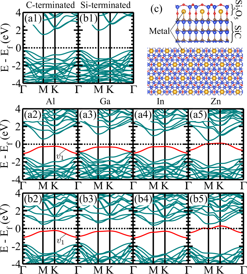
In this paper we explore the design of 2D lattices on the metal adsorbed oxidized silicon carbide surfaces. The metal (M) adatoms, with M=Al, Ga, In, and Zn, are patterned by the highly-ordered 2D silicate adlayer on the SiC surface, Si2O5/SiC [41; 42; 43; 44], giving rise to triangular metal lattices upon the formation of metal–surface chemical bonds embedded in Si2O5, (M)Si2O5/SiC, Fig. 1. We show that the 2D lattices can be constructed by the creation of metal vacancies on the surface. In particular, we have examined four 2D lattices, viz.: honeycomb, kagome and two lattices with higher pseudospin Dirac quasiparticles, however, our findings are not limited to those ones. Our electronic structure results reveal that the characteristic band structures of the 2D lattices are dictated by the metal- states (dominant contribution) hybridized with the host- orbitals, giving rise to Dirac bands neatly lying in the band gap of a semiconductor surface.
Results and Discussions. Silicate adlayer metallization.
We have considered oxidized SiC surfaces forming a () reconstructed Si2O5 silicate adlayer on the C [Si] terminated surface, Si2O5/SiC(000) [Si2O5/SiC(0001)]. The silicate/SiC interface is characterized by a hexagonal structure of O–C [O–Si] chemical bonds with the topmost atoms of the (000) [(0001)] surface, centered by a single C [Si] dangling bond per surface unit cell. The unpaired electron of the dangling bond gives rise to localized spin-polarized surface states (SSs) within the energy gap of SiC [46]. As shown in Fig. 1(a1) and (b1), such SSs are washed out from the energy gap by the hydrogen passivation of those dangling bonds. We found a gap of and eV for C and Si terminations, respectively; consistent with previous calculations [46; 45].
Instead of hydrogen, the passivation of the surface dangling bonds by post-transition metals, Al, Ga, In and Zn [Fig. 1(c)] will bring back the SSs; but now ruled by spherically symmetric orbitals of the metal adatoms hybridized with the host Si2O5/SiC surface. For instance, the passivation of the C [Si] dangling bond by an Al adatom, (Al)Si2O5/SiC(000) [(Al)Si2O5/SiC(0001)], the Al- electron will passivate the dangling bond. Meanwhile the Al- orbitals will give rise to a fully occupied SS lying within the band gap of SiC; indicated as in Figs. 1(a2) and 1(b2) for (Al)Si2O5/SiC(000) and (Al)Si2O5/SiC(0001), respectively. It is worth noting that presents an energy dispersion of about 1 eV for wave vectors parallel to the surface, indicating an electronic interaction between the Al adatoms mediated by the Si2O5/SiC host orbitals. Indeed, through the calculation of the projected electronic band structure (not shown) we find that the -orbital of the Al adatom hybridizes with the orbital of the surface (Si or C) dangling bond, and planar orbitals of the silicate layer. The latter rules for the electronic interaction between the nearest-neighbor (NN) Al adatoms. The same behavior has been observed for the same valence Ga, and In metals, Figs. 1(a3)-(b3) and 1(a4)-(b4) respectively. Moreover, for Zn atoms, which present one valence electron less than Al, a partially filled 4 state is predicted on the Fermi energy, as shown in Fig. 1(a5)-(b5).
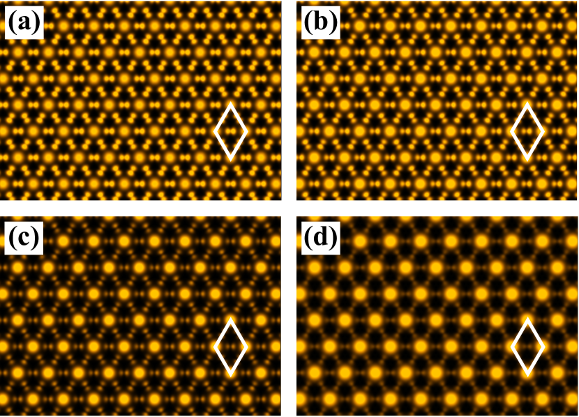
Further electronic structure characterization was performed by a set of STM simulations of the occupied states, shown in Fig. 2. Although the metal atoms lie below the topmost Si–O hexagonal lattice of the silicate layer, the simulated images are characterized by bright spots lying on the metal adatoms forming a triangular lattice connected by less intense bright lines. We are picturing the metal induced (-orbital) SSs, hybridized with the surface planar orbitals, giving rise to “electronic bonds” connecting the NN metal atoms.
| M/C-SiC(O) | ||||
|---|---|---|---|---|
| Configuration | Al | Ga | In | Zn |
| honeycomb () | 1.17 | 1.33 | 1.86 | 2.91 |
| kagome () | 1.43 | 1.61 | 2.22 | 3.41 |
| tri-rect () | 1.43 | 1.61 | 2.22 | 3.41 |
| snub-hex () | 1.78 | 1.98 | 2.69 | 4.05 |
| M/Si-SiC(O) | ||||
| Configuration | Al | Ga | In | Zn |
| honeycomb () | 1.86 | 1.87 | 2.38 | 2.99 |
| kagome () | 2.07 | 2.22 | 2.81 | 3.50 |
| tri-rect () | 2.07 | 2.22 | 2.81 | 3.50 |
| snub-hex () | 2.66 | 2.68 | 3.36 | 4.14 |
Design of 2D lattices.
Given such an electronic scenario, based on the SSs induced by the metal -orbital in the band gap of SiC, (M)Si2O5/SiC is an interesting and realistic semiconductor platform to design 2D lattices throughout the creation of metal vacancies on the surface [32; 47]. Indeed, in a recent study, we explored the electronic properties of Archimedean lattice models based in a 2D -orbital tight-binding model [15]. Here, we explore the electronic properties of triangular based lattices where the metal vacancy sites are saturated by hydrogen atoms, in order to preserve the semiconducting character of the Si2O5/SiC host surface.
Since the proposed lattice design is based on an atomic exchange between the metal atoms, embedded in (M)Si2O5/SiC, by hydrogen atoms passivating the remnant surface dangling bonds, the energetic stability of the final system was inferred through the following total energy comparison (),
| (1) |
where is the total energy of the (M)Si2O5/SiC surface with a given concentration () of metal atoms exchanged by hydrogen atoms (MH), is the number MH exchanged atoms, ( is the total number of sites); while is the total energy of the fully metallized surface, and () is the total energies of an isolated metal (hydrogen) atom. Our results of , summarized in Table 1, indicate that the MH atomic exchange processes are exothermic (), and thus supporting the feasibility of engineering 2D lattices on the (M)Si2O5/SiC semiconductor surfaces. Indeed, very recently, 2D atomic lattices based on “vacancy design” have been successfully synthesized on metal surface, clorine-monolayer/Cu(100) [32].
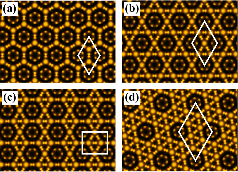
In order to illustrate the lattice formation, in Fig. 3 we present the simulated STM images of the occupied states, within an energy interval of 1 eV below the Fermi level of the (Al)Si2O5/SiC(000) surface. Here, we have considered the following triangular based lattices, honeycomb (=1/3), kagome (=1/4), triangular-rectangular (=1/4), and snub-hexagonal (=1/7), as depicted in Figs. 3(a)–3(d). It is worth noting that other 2D lattices can be designed on the (M)Si2O5/SiC surface, for instance, the ones predicted/synthesized based on boron atoms [48; 49; 50].
The STM pictures are characterized by dark spots on the AlH exchanged sites, since the electronic states of the C–H bonds are resonant within the valence and conduction bands of SiC. In contrast, the Al atoms are identified by the SSs composed Al- orbitals hybridized with the surface host orbitals. In this case, we find bright spots on the Al atoms, connected by “electronic bonds”, forming an artificial Al lattice on the Si2O5/SiC(000) surface. Similar STM results were obtained for the other (M)Si2O5/SiC systems.
We can estimate the inter-metal coupling due the “electronic bonds” by comparing the hopping strength () with the band width from a NN tight-binding model [51]. The coupling between the metals are insensitive to the surface termination, and the difference in by less then meV for same lattice and different terminations. We find and meV, for M = Al, Ga, In and Zn, respectively. These values are close to the experimentally achieved in the interacting lattice of chlorine layer on Cu(100) [32]. Such an interaction plays an important role on the electronic band structure of the 2D lattices on (M)Si2O5/SiC.
Lattice’s electronic structure.
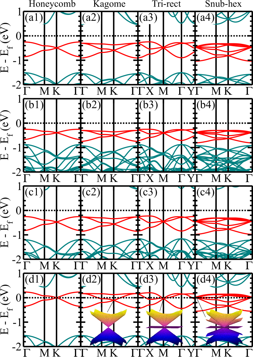
The electronic band structures of the (M)Si2O5/SiC surfaces, upon the MH atomic exchanges, can be considered as the fingerprints of the (proposed) artificial metal lattices. In panel (a1) of Figs. 4 and 5 we present the electronic band structure of (Al)Si2O5/SiC(000) and /SiC(0001) surfaces, where we have an artificial graphene-like structure of Al atoms. We find linear energy dispersions at the K-point, and the projection of those energy bands reveals that those Dirac bands are mostly composed by Al- orbitals hybridized with (i) the planar O- orbitals of silicate layers, and (ii) the orbitals of the topmost C/Si atoms of the SiC(000)/(0001) surface bonded to Al adatoms. The energy dispersion of those Dirac bands are mostly dictated by the overlap of Al- and O- orbitals [(i)]. Kagome energy bands, i.e. graphenelike energy bands forming a Dirac cone at the K-point, degenerated with a nearly flat band at the center of the Brillouin zone, are nicely reproduced for a artificial kagome lattice of Al atoms, panel (a2) of Figs. 4 and 5. Additionally, by constructing different lattices, we could achieve the pseudospin-1 and -2 Dirac quasiparticles [52; 8] at the M point and point of triangular-rectangular and snub-hexagonal lattices, respectively shown in panels (a3)-(c3) and (a4)-(c4) of Fig. 4 and Fig. 5. Different from the spin- Dirac equation, leading to the Dirac cone [see inset of Fig. 4(d2)], these quasiparticles generalize the Pauli matrix in the Dirac equation by the angular momentum matrix of higher spin [53; 54]. We can characterize the pseudospin-1 Dirac quasiparticle by a Dirac cone degenerated with a flat band [see inset of Fig. 4(d3)], while for the pseudospin-2 case two Dirac cones with velocities related by a factor of 2 are degenerated with a flat band [see inset of Fig. 4(d4)].
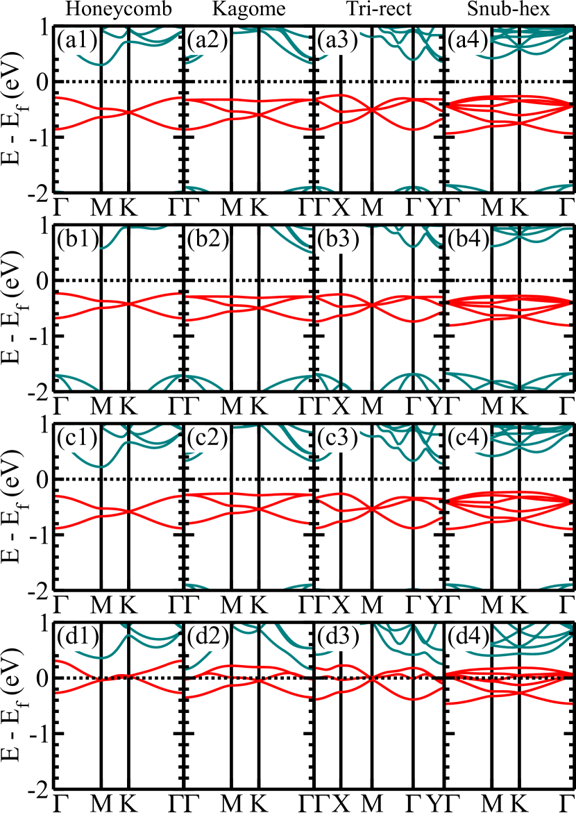
Since Ga and In atoms exhibit the same valence configuration, (Ga)Si2O5/ and (In)Si2O5/SiC exhibit nearly the same characteristic band structures as depicted in panels (a2)-(d2) and (a3)-(d4) of Figs. 4 and 5. In both (M)Si2O5/SiC systems, the characteristic bands are localized below the Fermi energy. Whereas, in (Zn)Si2O5/SiC the Zn- orbital gives rise to metallic bands, panels (d1)-(d4) in Fig. 4 and Fig. 5. In particular, for the Si terminated (Zn)Si2O5/SiC(0001) surface [Figs. 5(d1)-(d4)], the Zn- states are nearly resonant with the the edge of the SiC bulk conduction band. In this case, the energy dispersions of the characteristic bands become distorted, (i) the honeycomb lattice present additional crossing along M-K points besides the Dirac states at K point [Fig. 5(d1)], (ii) the kagome flat band bend upward [Fig. 5(d2)], and (iii) degeneracy breaking at point of triangular-rectangular and snub-hexagonal lattice are observed [Fig. 5(d3) and (d4)]. It is worth pointing out that we have performed calculations with spin-orbit coupling (SOC) in order to clarify its effect in the band structures. Here we found a small SOC effect, where due to the surface inversion symmetry breaking, a Rashba spliting from to of the band width been found with the highest value for (In)Si2O5/SiC(0001). Such scenario does not alter significantly the electronic structure of the systems, which preserve its characteristic band dispersion.
In summary, we have explored the design of 2D lattices based on incorporation/removal of metal (M) adatoms patterned by ordered silicate adlayer on the SiC surface, (M)Si2O5/SiC. Here, the metal adatoms are caged (protected) within the silicate adlayer, where we demonstrate that the metals can still be observed in STM experiments. We shown that Al, Ga, In and Zn metal atoms present their valence states within the substrate energy gap, allowing an exploration of lattices’ electronic structure. As a proof of principle, we characterize the arising (i) relativistic Dirac states in a honeycomb lattice, (ii) flat bands in a kagome lattice, and (iii) pseudospin-1 and 2 in a triangular-rectangular and snub-hexagonal lattices, respectively; however, our findings can be extended to other 2D lattices on the Si2O5/SiC surface.
Computational approach.
We have performed first-principle calculations, within density functional theory, as implemented in the plane wave based VASP code [55]. The exchange and correlation was described by Perdew, Burke, and Ernzerhof (PBE) functional [56], with the plane wave basis with 400 eV cutoff energy. We have considered the SiC(0001) and SiC(000) slabs with six atomic layers, with one side bonded to the silica Si2O5 and the other hydrogen passivated. The electron-ion interaction was taken into account throughout the projector augmented wave method (PAW) [57]. All atoms positions have been relaxed until all forces were less then meV/Å, within a k-mesh of special points [58], where is the supercell multiplicity (for the unity cell ). For the band structure calculations a increased k-mesh of have been considered.
ACKNOWLEDGMENTS
The authors acknowledge financial support from the Brazilian agencies CNPq, CAPES, and FAPEMIG, and the CENAPAD-SP and Laboratório Nacional de Computação Científica (LNCC-SCAFMat2) for computer time.
References
- Geim and Novoselov [2007] A. K. Geim and K. S. Novoselov, Nature Materials 6, 183 (2007).
- Mounet et al. [2018] N. Mounet, M. Gibertini, P. Schwaller, D. Campi, A. Merkys, A. Marrazzo, T. Sohier, I. E. Castelli, A. Cepellotti, G. Pizzi, and N. Marzari, Nature Nanotechnology 13, 246 (2018).
- Haastrup et al. [2018] S. Haastrup, M. Strange, M. Pandey, T. Deilmann, P. S. Schmidt, N. F. Hinsche, M. N. Gjerding, D. Torelli, P. M. Larsen, A. C. Riis-Jensen, J. Gath, K. W. Jacobsen, J. J. Mortensen, T. Olsen, and K. S. Thygesen, 2D Materials 5, 042002 (2018).
- Geng and Yang [2018] D. Geng and H. Y. Yang, Advanced Materials 30, 1800865 (2018).
- Lan et al. [2011] Z. Lan, N. Goldman, A. Bermudez, W. Lu, and P. Öhberg, Phys. Rev. B 84, 165115 (2011).
- Wang et al. [2018] A. Wang, X. Zhao, M. Zhao, X. Zhang, Y. Feng, and F. Liu, The Journal of Physical Chemistry Letters 9, 614 (2018).
- Wang et al. [2019] Z. F. Wang, B. Liu, and W. Zhu, Phys. Rev. Lett. 123, 126403 (2019).
- Crasto de Lima and Ferreira [2020] F. Crasto de Lima and G. J. Ferreira, Phys. Rev. B 101, 041107 (2020).
- Lu et al. [2014] L. Lu, J. D. Joannopoulos, and M. Soljacic, Nature Photonics 8, 821 (2014).
- Zhu et al. [2018] Z. Zhu, Y. Liu, Z.-M. Yu, S.-S. Wang, Y. X. Zhao, Y. Feng, X.-L. Sheng, and S. A. Yang, Phys. Rev. B 98, 125104 (2018).
- Gao et al. [2018] W. Gao, X. Zhu, F. Zheng, M. Wu, J. Zhang, C. Xi, P. Zhang, Y. Zhang, N. Hao, W. Ning, and M. Tian, Nature Communications 9, 3249 (2018).
- Kane and Mele [2005] C. L. Kane and E. J. Mele, Phys. Rev. Lett. 95, 226801 (2005).
- Hatsuda et al. [2018] K. Hatsuda, H. Mine, T. Nakamura, J. Li, R. Wu, S. Katsumoto, and J. Haruyama, Science Advances 4, eaau6915 (2018).
- Ostrovsky et al. [2008] P. M. Ostrovsky, I. V. Gornyi, and A. D. Mirlin, Phys. Rev. B 77, 195430 (2008).
- Crasto de Lima et al. [2018] F. Crasto de Lima, G. J. Ferreira, and R. H. Miwa, Phys. Chem. Chem. Phys. 20, 22652 (2018).
- Komatsu et al. [2018] K. Komatsu, Y. Morita, E. Watanabe, D. Tsuya, K. Watanabe, T. Taniguchi, and S. Moriyama, Science Advances 4, eaaq0194 (2018).
- Snyder and Toberer [2008] G. J. Snyder and E. S. Toberer, Nature Materials 7, 105 (2008).
- Ang et al. [2017] Y. S. Ang, S. A. Yang, C. Zhang, Z. Ma, and L. K. Ang, Phys. Rev. B 96, 245410 (2017).
- Naghavi et al. [2018] S. S. Naghavi, J. He, Y. Xia, and C. Wolverton, Chemistry of Materials 30, 5639 (2018).
- Dong et al. [2019] B. Dong, Z. Wang, N. T. Hung, A. R. Oganov, T. Yang, R. Saito, and Z. Zhang, Phys. Rev. Materials 3, 013405 (2019).
- Crasto de Lima et al. [2019a] F. Crasto de Lima, G. J. Ferreira, and R. H. Miwa, The Journal of Chemical Physics 150, 234701 (2019a).
- Räsänen et al. [2012] E. Räsänen, C. A. Rozzi, S. Pittalis, and G. Vignale, Phys. Rev. Lett. 108, 246803 (2012).
- Gibertini et al. [2009] M. Gibertini, A. Singha, V. Pellegrini, M. Polini, G. Vignale, A. Pinczuk, L. N. Pfeiffer, and K. W. West, Phys. Rev. B 79, 241406 (2009).
- Polini et al. [2013] M. Polini, F. Guinea, M. Lewenstein, H. C. Manoharan, and V. Pellegrini, Nature Nanotechnology 8, 625 (2013).
- Colson and Dichtel [2013] J. W. Colson and W. R. Dichtel, Nature Chemistry 5, 453 (2013).
- Rodríguez-San-Miguel et al. [2016] D. Rodríguez-San-Miguel, P. Amo-Ochoa, and F. Zamora, Chem. Commun. 52, 4113 (2016).
- Baumann et al. [2019] A. E. Baumann, D. A. Burns, B. Liu, and V. S. Thoi, Communications Chemistry 2, 86 (2019).
- Crommie et al. [1993] M. F. Crommie, C. P. Lutz, and D. M. Eigler, Science 262, 218 (1993).
- Celotta et al. [2014] R. J. Celotta, S. B. Balakirsky, A. P. Fein, F. M. Hess, G. M. Rutter, and J. A. Stroscio, Review of Scientific Instruments 85, 121301 (2014).
- Pavlicek et al. [2017] N. Pavlicek, A. Mistry, Z. Majzik, N. Moll, G. Meyer, D. J. Fox, and L. Gross, Nature Nanotechnology 12, 308 (2017).
- Slot et al. [2019] M. R. Slot, S. N. Kempkes, E. J. Knol, W. M. J. van Weerdenburg, J. J. van den Broeke, D. Wegner, D. Vanmaekelbergh, A. A. Khajetoorians, C. Morais Smith, and I. Swart, Phys. Rev. X 9, 011009 (2019).
- Drost et al. [2017] R. Drost, T. Ojanen, A. Harju, and P. Liljeroth, Nature Physics 13, 668 (2017).
- Slot et al. [2017] M. R. Slot, T. S. Gardenier, P. H. Jacobse, G. C. P. van Miert, S. N. Kempkes, S. J. M. Zevenhuizen, C. M. Smith, D. Vanmaekelbergh, and I. Swart, Nature Physics 13, 672 (2017).
- Gomes et al. [2012] K. K. Gomes, W. Mar, W. Ko, F. Guinea, and H. C. Manoharan, Nature 483, 306 (2012).
- Collins et al. [2017] L. C. Collins, T. G. Witte, R. Silverman, D. B. Green, and K. K. Gomes, Nature Communications 8, 15961 (2017).
- Kempkes et al. [2019] S. N. Kempkes, M. R. Slot, S. E. Freeney, S. J. M. Zevenhuizen, D. Vanmaekelbergh, I. Swart, and C. M. Smith, Nature Physics 15, 127 (2019).
- Presser and Nickel [2008] V. Presser and K. G. Nickel, Critical Reviews in Solid State and Materials Sciences 33, 1 (2008).
- Wang et al. [2015] G. Wang, G. C. Loh, R. Pandey, and S. P. Karna, The Journal of Physical Chemistry C 119, 15654 (2015).
- Büchner et al. [2014] C. Büchner, L. Lichtenstein, S. Stuckenholz, M. Heyde, F. Ringleb, M. Sterrer, W. E. Kaden, L. Giordano, G. Pacchioni, and H.-J. Freund, The Journal of Physical Chemistry C 118, 20959 (2014).
- Büchner and Heyde [2017] C. Büchner and M. Heyde, Progress in Surface Science 92, 341 (2017).
- Bernhardt et al. [1999] J. Bernhardt, J. Schardt, U. Starke, and K. Heinz, Applied Physics Letters 74, 1084 (1999).
- Schürmann et al. [2006] M. Schürmann, S. Dreiner, U. Berges, and C. Westphal, Phys. Rev. B 74, 035309 (2006).
- Hoshino et al. [2004] Y. Hoshino, R. Fukuyama, and Y. Kido, Phys. Rev. B 70, 165303 (2004).
- Tochihara et al. [2014] H. Tochihara, T. Shirasawa, T. Suzuki, T. Miyamachi, T. Kajiwara, K. Yagyu, S. Yoshizawa, T. Takahashi, S. Tanaka, and F. Komori, Applied Physics Letters 104, 051601 (2014).
- Padilha et al. [2019] J. Padilha, R. Pontes, F. C. de Lima, R. Kagimura, and R. Miwa, Carbon 145, 603 (2019).
- Lu et al. [2000] W. Lu, P. Krüger, and J. Pollmann, Phys. Rev. B 61, 13737 (2000).
- Yan and Liljeroth [2019] L. Yan and P. Liljeroth, Advances in Physics: X 4, 1651672 (2019).
- Penev et al. [2012] E. S. Penev, S. Bhowmick, A. Sadrzadeh, and B. I. Yakobson, Nano Letters 12, 2441 (2012).
- Zhang et al. [2015] Z. Zhang, Y. Yang, G. Gao, and B. I. Yakobson, Angewandte Chemie International Edition 54, 13022 (2015).
- Crasto de Lima et al. [2019b] F. Crasto de Lima, G. J. Ferreira, and R. H. Miwa, Nano Letters 19, 6564 (2019b).
- Bena and Montambaux [2009] C. Bena and G. Montambaux, New Journal of Physics 11, 095003 (2009).
- Crasto de Lima et al. [2019c] F. Crasto de Lima, G. J. Ferreira, and R. H. Miwa, Phys. Chem. Chem. Phys. 21, 22344 (2019c).
- Urban et al. [2011] D. F. Urban, D. Bercioux, M. Wimmer, and W. Häusler, Phys. Rev. B 84, 115136 (2011).
- Fang et al. [2019] A. Fang, S. G. Louie, and C. T. Chan, Research 2019, 3054062 (2019).
- Kresse and Furthmüller [1996] G. Kresse and J. Furthmüller, Computational Materials Science 6, 15 (1996).
- Perdew et al. [1996] J. P. Perdew, K. Burke, and M. Ernzerhof, Phys. Rev. Lett. 77, 3865 (1996).
- Blöchl [1994] P. E. Blöchl, Phys. Rev. B 50, 17953 (1994).
- Monkhorst and Pack [1976] H. J. Monkhorst and J. D. Pack, Phys. Rev. B 13, 5188 (1976).