Extraordinary magnetoresistance in encapsulated monolayer graphene devices
Abstract
We report a proof-of-concept study of extraordinary magnetoresistance (EMR) in devices of monolayer graphene encapsulated in hexagonal boron nitride, having metallic edge contacts and a central metal shunt. Extremely large EMR values, , are achieved in part because approaches or crosses zero as a function of the gate voltage, exceeding that achieved in high mobility bulk semiconductor devices. We highlight the sensitivity, , which in two-terminal measurements is the highest yet reported for EMR devices, and in particular exceeds prior results in graphene-based devices by a factor of 20. An asymmetry in the zero-field transport is traced to the presence of -junctions at the graphene-metal shunt interface.
The extraordinary magnetoresistance (EMR) effect discovered by Solin and coworkers led to widespread interest in this phenomenon for magnetic sensing applications Solin et al. (2000, 2002); Hewett and Kusmartsev (2012); Sun and Kosel (2013). In the original work Solin et al. (2000), an extremely large magnetoresistance was found with the normalized ratio as high as 16,000 111 values are often reported as a % change. In this work we report the ratio itself. at T, in devices comprised of a four-terminal InSb disk with a central metal shunt. EMR is a geometric effect: at zero field, the shunt short circuits current through the middle of the device. However in a perpendicular field the charge carriers are deflected around the shunt as the current density becomes orthogonal to the interfacial electric field at the interface of the shunt and the semiconductor. Charge carriers are forced to travel through the more resistive material around the shunt, leading to a magnetoresistance enhanced over the zero field value by up to several orders of magnitude. Refinements to the original devices enable detectors suitable for fine-scale magnetic field sensors Zhou, Hines, and Solin (2001); Solin et al. (2002); Sun, Gooneratne, and Kosel (2012). EMR can be enhanced by tailoring the shape of the shunt and also by asymmetries in the overall device configuration Solin and Zhou (2001); Hewett and Kusmartsev (2010); Pugsley, Ram-Mohan, and Solin (2013).
The advent of graphene device research in 2004 introduced a material with a readily tunable, bipolar conductivity, and was soon followed by a first generation of graphene EMR devices Novoselov et al. (2004); Pisana et al. (2010a, b); Friedman et al. (2011); Lu et al. (2011); El-Ahmar et al. (2017). While an EMR effect was achieved, the ratios remained below 1000, well short of that in bulk semiconductors. Recently, significant improvement in graphene device quality has been achieved by encapsulating graphene in flakes of hexagonal boron nitride (hBN), an atomically-flat 6-eV-gap insulator Kubota et al. (2007). The hBN protects graphene from extrinsic disorder, leading to very high quality transport Dean et al. (2010); Wang et al. (2013). With device mobility linked to greater EMR Solin et al. (2000); Hewett and Kusmartsev (2012), here we investigate EMR devices fabricated from encapsulated graphene. For comparison, the InSb devices used by Solin et al. typically have mobilities of cm2/Vs Solin et al. (2000); graphene-on-oxide devices are in the 1,000 to 10,000 cm2/Vs range but the mobilities of hBN-encapsulated devices can be 2 or 3 orders of magnitude larger Pisana et al. (2010a, b); Friedman et al. (2011); Lu et al. (2011); El-Ahmar et al. (2017); Dean et al. (2010); Wang et al. (2013).
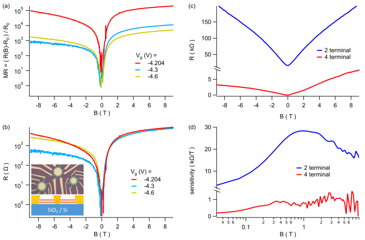
The EMR devices here are made of flakes of monolayer graphene sandwiched between -nm-thick hBN flakes, assembled into stacks by a dry-transfer technique Wang et al. (2013). The device geometry is defined by reactive ion etching to create a disk with outer radius having a concentric circular hole of radius . Films of Ti/Al, 4/80 nm thick, produce electrical contacts to the outer edge and a central metal shunt contacting graphene around the inner perimeter, as shown inset to Fig. 1(b). Electronic transport measurements were made by standard lockin techniques with a V bias at 13 Hz, at 300 K in a 9 T solenoid. Unless otherwise specified, all data is acquired in a four-terminal configuration. The graphene carrier density and conductivity are precisely controlled by a gate voltage applied to the Si substrate. The density, V-1cm-2, is calibrated by measurements in nearby Hall devices lacking the central shunt. Varying ratios of the metallic shunt to outer radius are used with corresponding to a device without the metal shunt.
Figure 1a shows from the device with the largest observed effect, for three closely spaced gate voltages which, though corresponding to very small changes in the carrier density of the device, nonetheless exhibit a remarkable variation in magnitude of the EMR. The high ratio of exceeds that of bulk 3D semiconductor devices (for a circular geometry; alternative geometries may yield much higher values Pugsley, Ram-Mohan, and Solin (2013)). We also show in Fig. 1(b) the as-measured resistance, , for the same three traces as Fig. 1(a) showing that, at least for positive -field, the traces overlap almost identically. Thus, the variation of with must be due to changes in the value of . For reference below, this device had an outer radius of m and a radius ratio of 0.85.
Typically, circular EMR devices are measured using four contacts spaced at 90∘ relative to each other, and where possible this standard was followed here (e.g. in Fig. 1). In several devices, design constraints or lost contacts led to the use of contacts clustered within less than half the circumference of each device (as for data in Fig. 2). The metallic shunt is not always concentric with the outer device radius. Such non-idealities can lead to asymmetry in the EMR Solin and Zhou (2001), and may be responsible for the observed asymmetry between positive and negative magnetic fields. However, this does not alter our findings: the results of Fig. 1 are obtained in the standard geometry, while those of Figs. 2 and 3 are comparisons between samples with similar contact configurations.
While the ratio is a standard figure-of-merit, the sensitivity may be more useful as it captures the field-dependent response of the device, and is not sensitive to . This is helpful for devices that 1) have a nonlinear response to , and 2) have a gate-dependent . Thus in addition to the , we also plot in Fig. 1(c) and d the measured and corresponding (determined by numerical differentiation, which accounts for the high frequency noise in Fig. 1(d) ) in a single device, the same as for Fig. 1(a) and (b), at V. Results are shown for both a 2- or 4-terminal configuration. Two features stand out: first, the 2-terminal sensitivity is nearly twenty times larger than previously reported for graphene Lu et al. (2011) and sixty times larger than the highest reported value in semiconductor structures Sun et al. (2012). Second, the 2-terminal sensitivity greatly exceeds the 4-terminal values in the same device at the same . The reason has been previously discussed Sun, Gooneratne, and Kosel (2012) and a smaller instance was observed in Ref. Lu et al. (2011). The idea is straightforward: the farther the voltage probes are from the current contacts, the smaller the measured potential drop since the shunt enforces an equipotential at its edge. Therefore when the voltage probes approach and merge with the current contacts, the potential drop in the resulting two-terminal geometry reaches a maximum. These sensitivities exceed those of Hall sensors based on encapsulated graphene devices Dauber et al. (2015). We note that encapsulated graphene devices are a technology that is still improving rapidly, with recent advances in limiting the role of scattering by using nearby graphite gates Zibrov et al. (2017), and implementing 2D contacts by XeF2 etching of the hBN layers Son et al. (2018) which may greatly reduce the contact resistance and improve contact reproducibility. Neither approach is employed in the present study, suggesting that further improvements in device performance are achievable.
We use this result to estimate the achievable field resolution, . The resistance resolution is estimated to be the standard deviation of the measured resistance due to noise. For the 2- and 4-terminal data, and , respectively, leading to estimated peak resolutions of mT and mT with a one second averaging time. These values can be improved by e.g. longer meaurement times or impedance-matched preamplifiers.
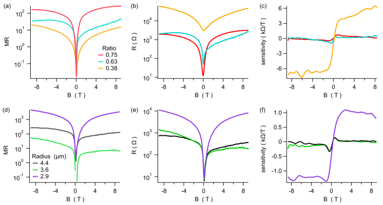
In Figure 2 we compare the ratio, measured resistance, and four-terminal sensitivity for two sets of devices. Panels (a-c) show results for a fixed outer radius of m and a varying shunt-to-outer radius ratio , while in Fig. 2(d)-(f) the ratio is held at 0.75 and the outer radius is varied. For all traces the gate voltage was held near charge neutrality of the graphene. The EMR is largest for the highest ratio, similar to prior work Solin and Zhou (2001). However, the largest device resistance and sensitivity are found for the smallest ratio. This highlights the role of in determining the magnitude of , while the sensitivity responds to the steepest change of which is independent of . The data for varying the overall radius is less conclusive: while the device with the smallest radius gives the largest response across the board, the other traces do not reveal a clear size dependence.
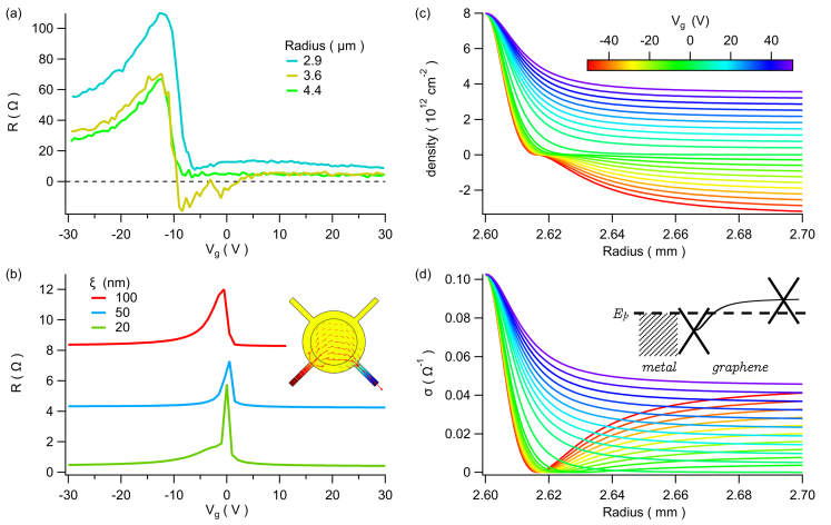
In principle an advantage of graphene-based EMR devices is the inherent tunability of graphene via . In graphene devices without a shunt, the resistance reaches a maximum at charge neutrality and falls off for increasing electron or hole charge density Novoselov et al. (2004). In shunted graphene-on-oxide devices, the maximum survives but is rather broad Pisana et al. (2010a, b); Lu et al. (2011); Friedman et al. (2011). In contrast, here the resistance maximum survives but invariably shows a strong asymmetry near charge neutrality; equally important, the resistance can become negative. An example is shown in Fig. 3(a), showing zero-field transport in three devices having the same ratio but different outer radii. In encapsulated graphene devices, the carrier mean free path can be m even at room temperature Wang et al. (2013), approximately the spacing between the shunt and outer radius of our devices. Thus transport becomes quasi-ballistic and “negative” resistances can arise due to non-diffusive transport Wang et al. (2013); Solin et al. (2002). In such a device can be tuned to zero, yielding an infinite ; this is a key reason for using sensitivity as a figure of merit.
The origin of the asymmetry in the zero-field resistance vs is likely due to the band re-alignment that occurs near a metal-graphene interface. This issue has been extensively investigated in the context of electrical contacts to graphene Giovannetti et al. (2008); Khomyakov et al. (2009); Mueller et al. (2009); Matsuda, Deng, and Goddard (2010); Xia et al. (2011); Allain et al. (2015). Briefly, the large density of states in the metal pins the Fermi level in graphene so it is highly doped (with most metals yielding -type doping) near the contact. But in the bulk of graphene, is still controlled by . Since the polarity at the metal-graphene interface is fixed, a -junction arises near the contacts depending on the charge state in the graphene bulk, effectively increasing the shunt contact resistance. Thus an asymmetry in the device behavior is expected as a function of .
To verify this picture we model transport through an EMR device assuming an edge-contacted geometry for the metal-graphene interface. Here one expects better overlap of the metal and carbon orbitals than for surface-contacted graphene, where the metal atoms encounter graphene orbitals that will not form covalent bonds Matsuda, Deng, and Goddard (2010). In models of surface-contacted graphene, this weak coupling allows the graphene Fermi level to move in response to , even for graphene directly under the metal Xia et al. (2011). In the present case, we assume the graphene density is pinned by the metal at the interface, no matter the in the bulk. Thus the potential relaxes over a characteristic distance from the interface back to the bulk value set by . Following Xia et al. Xia et al. (2011), the potential relaxation is
where is the radial position, the position dependence of the Fermi energy relative to charge neutrality in graphene, is the -controlled Fermi energy in the bulk, and is the work function difference of the metal and graphene. We use eV Khomyakov et al. (2009), and calculate the carrier density profile with the band velocity m/s. We then use finite element simulation to determine the total resistance of an EMR device with a metallic shunt and a gate-voltage-dependent graphene conductivity that varies spatially with the density as .
In Fig. 3(b) we show the results of this simple model, plotting the predicted zero-field resistance vs applied gate voltage for three values of the width . A clear similarity to the lineshape of the data in Fig. 3(a) is achieved, with best results for nm: the asymmetry appears, over a gate voltage range not much less than we observe, and the variation in resistance is, if not close, at least of similar magnitude. The most significant departure is in the value at the resistance peak. However, the peak location is sensitive to charge doping by extrinsic sources which we do not attempt to capture in this model. Figure 3(c) and (d) show the density and conductivity profiles for a range of , in a model geometry with m. As expected, for when the graphene bulk is -type, the conductivity reaches a minimum a short distance away from the graphene-metal interface due to the -junction. Thus the overall device resistance reflects the fact that the low-impedance path through the shunt is effectively shielded by the -junction when the bulk of graphene is doped opposite to that induced by the metal interface.
In conclusion, we have investigated the EMR effect in encapsulated graphene devices. We find the magnetoresistance can be enhanced by over four orders of magnitude from its zero field value, with an ratio that can surpass the highest reported for a circular device geometry. We also find very large values of the sensitivity, , reaching nearly k/T. An asymmetry in the gate voltage response of the zero-field resistance is traced to the presence of -junctions near the graphene-metal interface, and a model of edge-contacted graphene is in reasonable agreement with these observations. Encapsulated graphene is thus a promising platform for high-sensitivity measurements of magnetic fields using the EMR effect.
Acknowledgements.
We thank S. Solin for inspiration and a close reading of the manuscript, and gratefully acknowledge support from the Institute of Materials Science and Engineering at Washington University. EAH acknowledges partial support under NSF DMR-1810305.References
- Solin et al. (2000) S. A. Solin, T. Thio, D. R. Hines, and J. J. Heremans, “Enhanced room-temperature geometric magnetoresistance in inhomogeneous narrow-gap semiconductors,” Science 289, 1530–1532 (2000).
- Solin et al. (2002) S. A. Solin, D. R. Hines, A. C. H. Rowe, J. S. Tsai, Y. A. Pashkin, S. J. Chung, N. Goel, and M. B. Santos, “Nonmagnetic semiconductors as read-head sensors for ultra-high-density magnetic recording,” Applied Physics Letters 80, 4012–4014 (2002).
- Hewett and Kusmartsev (2012) T. Hewett and F. Kusmartsev, “Extraordinary magnetoresistance: sensing the future,” Central European Journal of Physics 10, 602–608 (2012).
- Sun and Kosel (2013) J. Sun and J. Kosel, “Extraordinary magnetoresistance in semiconductor/metal hybrids: A review,” Materials 6, 500–516 (2013).
- Note (1) values are often reported as a % change. In this work we report the ratio itself.
- Zhou, Hines, and Solin (2001) T. Zhou, D. R. Hines, and S. A. Solin, “Extraordinary magnetoresistance in externally shunted van der pauw plates,” Applied Physics Letters 78, 667–669 (2001).
- Sun, Gooneratne, and Kosel (2012) J. Sun, C. P. Gooneratne, and J. Kosel, “Design study of a bar-type emr device,” IEEE Sensors Journal 12, 1356–1360 (2012).
- Solin and Zhou (2001) S. A. Solin and T. Zhou, “Extraordinary magnetoresistance of an off-center van der pauw disk,” in International Conference on Solid State Devices and Materials (The Japan Society of Applied Physics, 2001) p. 570.
- Hewett and Kusmartsev (2010) T. H. Hewett and F. V. Kusmartsev, “Geometrically enhanced extraordinary magnetoresistance in semiconductor-metal hybrids,” Physical Review B 82, 212404 (2010).
- Pugsley, Ram-Mohan, and Solin (2013) L. M. Pugsley, L. R. Ram-Mohan, and S. A. Solin, “Extraordinary magnetoresistance in two and three dimensions: Geometrical optimization,” Journal of Applied Physics 113, 064505 (2013).
- Novoselov et al. (2004) K. S. Novoselov, A. K. Geim, S. V. Morozov, D. Jiang, Y. Zhang, S. V. Dubonos, I. V. Grigorieva, and A. A. Firsov, “Electric field effect in atomically thin carbon films,” Science 306, 666 (2004).
- Pisana et al. (2010a) S. Pisana, P. M. Braganca, E. E. Marinero, and B. A. Gurney, “Graphene magnetic field sensors,” IEEE Transactions on Magnetics 46, 1910–1913 (2010a).
- Pisana et al. (2010b) S. Pisana, P. M. Braganca, E. E. Marinero, and B. A. Gurney, “Tunable nanoscale graphene magnetometers,” Nano Letters 10, 341–346 (2010b).
- Friedman et al. (2011) A. L. Friedman, J. T. Robinson, F. K. Perkins, and P. M. Campbell, “Extraordinary magnetoresistance in shunted chemical vapor deposition grown graphene devices,” Applied Physics Letters 99, 022108 (2011).
- Lu et al. (2011) J. Lu, H. Zhang, W. Shi, Z. Wang, Y. Zheng, T. Zhang, N. Wang, Z. Tang, and P. Sheng, “Graphene magnetoresistance device in van der pauw geometry,” Nano Letters 11, 2973–2977 (2011).
- El-Ahmar et al. (2017) S. El-Ahmar, W. Koczorowski, A. A. Poźniak, P. Kuświk, W. Strupiński, and R. Czajka, “Graphene-based magnetoresistance device utilizing strip pattern geometry,” Applied Physics Letters 110, 043503 (2017).
- Kubota et al. (2007) Y. Kubota, K. Watanabe, O. Tsuda, and T. Taniguchi, “Deep ultraviolet light-emitting hexagonal boron nitride synthesized at atmospheric pressure,” Science 317, 932 (2007).
- Dean et al. (2010) C. R. Dean, A. F. Young, I. Meric, C. Lee, L. Wang, S. Sorgenfrei, K. Watanabe, T. Taniguchi, P. Kim, K. L. Shepard, and J. Hone, “Boron nitride substrates for high-quality graphene electronics,” Nature Nanotechnology 5, 722–726 (2010).
- Wang et al. (2013) L. Wang, I. Meric, P. Y. Huang, Q. Gao, Y. Gao, H. Tran, T. Taniguchi, K. Watanabe, L. M. Campos, D. A. Muller, J. Guo, P. Kim, J. Hone, K. L. Shepard, and C. R. Dean, “One-dimensional electrical contact to a two-dimensional material,” Science 342, 614–617 (2013).
- Sun et al. (2012) J. Sun, S. B. Patil, Y.-A. Soh, and J. Kosel, “Strong temperature dependence of extraordinary magnetoresistance correlated to mobility in a two-contact device,” Applied Physics Express 5, 033002 (2012).
- Dauber et al. (2015) J. Dauber, A. A. Sagade, M. Oellers, K. Watanabe, T. Taniguchi, D. Neumaier, and C. Stampfer, “Ultra-sensitive Hall sensors based on graphene encapsulated in hexagonal boron nitride,” Applied Physics Letters 106, 193501 (2015).
- Zibrov et al. (2017) A. A. Zibrov, C. Kometter, H. Zhou, E. M. Spanton, T. Taniguchi, K. Watanabe, M. P. Zaletel, and A. F. Young, “Tunable interacting composite fermion phases in a half-filled bilayer-graphene landau level,” Nature 549, 360–364 (2017).
- Son et al. (2018) J. Son, J. Kwon, S. Kim, Y. Lv, J. Yu, J.-Y. Lee, H. Ryu, K. Watanabe, T. Taniguchi, R. Garrido-Menacho, N. Mason, E. Ertekin, P. Y. Huang, G.-H. Lee, and A. M. van der Zande, “Atomically precise graphene etch stops for three dimensional integrated systems from two dimensional material heterostructures,” Nature Communications 9, 3988 (2018).
- Giovannetti et al. (2008) G. Giovannetti, P. Khomyakov, G. Brocks, V. Karpan, J. van den Brink, and P. Kelly, “Doping graphene with metal contacts,” Physical Review Letters 101, 026803 (2008).
- Khomyakov et al. (2009) P. A. Khomyakov, G. Giovannetti, P. C. Rusu, G. Brocks, J. van den Brink, and P. J. Kelly, “First-principles study of the interaction and charge transfer between graphene and metals,” Physical Review B 79, 195425 (2009).
- Mueller et al. (2009) T. Mueller, F. Xia, M. Freitag, J. Tsang, and P. Avouris, “Role of contacts in graphene transistors: A scanning photocurrent study,” Physical Review B 79, 245430 (2009).
- Matsuda, Deng, and Goddard (2010) Y. Matsuda, W.-Q. Deng, and W. A. Goddard, “Contact resistance for “end-contacted” metal-graphene and metal-nanotube interfaces from quantum mechanics,” The Journal of Physical Chemistry C 114, 17845–17850 (2010).
- Xia et al. (2011) F. Xia, V. Perebeinos, Y.-M. Lin, Y. Wu, and P. Avouris, “The origins and limits of metal-graphene junction resistance,” Nature Nanotechnology 6, 179–184 (2011).
- Allain et al. (2015) A. Allain, J. Kang, K. Banerjee, and A. Kis, “Electrical contacts to two-dimensional semiconductors,” Nature Materials 14, 1195–1205 (2015).