Material design with the van der Waals stacking of bismuth-halide chains realizing a higher-order topological insulator
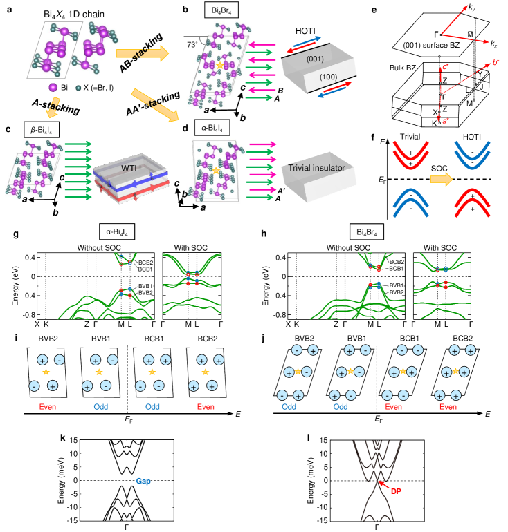
The van der Waals (vdW) materials with low dimensions have been extensively studied as a platform to generate exotic quantum properties [1, 2, 3, 4, 5, 6]. Advancing this view, a great deal of attention is currently paid to topological quantum materials with vdW structures. Here, we provide a new concept of designing topological materials by the vdW stacking of quantum spin Hall insulators (QSHIs). Most interestingly, a slight shift of inversion center in the unit cell caused by a modification of stacking is found to induce the topological variation from a trivial insulator to a higher-order topological insulator (HOTI). Based on that, we present the first experimental realization of a HOTI by investigating a bismuth bromide Bi4Br4 [7, 8, 9, 10, 11, 12] with angle-resolved photoemission spectroscopy (ARPES). The unique feature in bismuth halides capable of selecting various topology only by differently stacking chains, combined with the great advantage of the vdW structure, offers a fascinating playground for engineering topologically non-trivial edge-states toward future spintronics applications.
The weak topological insulator (WTI) phases have been confirmed in the materials with stacked QSHI layers, where the side-surface becomes topologically non-trivial by accumulating helical edge states of QSHI layers [13, 14]. Similarly, higher-order topological insulators (HOTIs) are expected to be built from stacking QSHIs, which, however, accumulate the 1D edge-states to develop 1D helical hinge-states in a 3D crystal [15, 16]. Such HOTI phases have been theoretically predicted recently in materials previously regarded as trivial insulators under the criterion by extending the topological classification to the topological index [17, 18, 19, 20, 21, 22]. To date, only one material has been experimentally confirmed to be in the higher-order topological phase, which is bulk bismuth [23]. However, bulk bismuth is a semimetal, which cannot become insulating even by carrier doping. Materials science is, therefore, awaiting the first experimental realization of a HOTI, which enables one to explore various quantum phenomena including spin currents around hinges and quantized conductance under the external fields.
A quasi-1D bismuth bromide, Bi4Br4, with a bilayer structure of chains (Fig. 1b) is theoretically predicted to be a topological crystalline insulator of , protected by the -rotation symmetry [19, 20, 21, 11, 12, 10]. This state should develop 2D topological surface states in the cross-section (010) of the chains [24, 25]. Significantly, theory also categorizes this system as a HOTI, and expects that 1D helical hinge-states emerge between the top-surface (001) and the side-surface (100) of a crystal due to the second-order bulk-boundary correspondence [11, 12]. Nevertheless, the topological phase of Bi4Br4 has not been experimentally revealed so far, and thus spectroscopic measurements are necessary to identify that Bi4Br4 is indeed a HOTI.
Here we propose that the quasi-1D bismuth halides [7, 8] offers an excellent platform to realize various topological phases selected by different stacking structures of the Bi4 (=I or Br) chains (Figs. 1a-d). A WTI state emerges in -Bi4I4 with single-layered chains per unit cell (A-stacking; Fig. 1c), in which quasi-1D topological surface states have been observed in the side surface of the crystal [14]. A trivial insulator phase is instead obtained in -Bi4I4, where the chains take a double-layered structure (AA’-stacking; Fig. 1d). While a HOTI candidate Bi4Br4 also consists of double layers, one of these is flipped by 180∘ in the unit cell (AB-stacking; Fig. 1b), indicating that the difference in stacking induces the topological phase variation from a trivial insulator to a HOTI.
To understand the difference of the topological class between the AA’- and AB-stacking, we have conducted DFT calculations for -Bi4I4 and Bi4Br4 (Figs. 1g and h, respectively). A critical difference between the two compounds is seen in the order of parity eigenvalues before the inclusion of the spin-orbit coupling (SOC) at the L point (left panels in Figs. 1g and h): the bilayer-split states near of Bi4Br4 have the same signs in the parities, [], for the bulk valence bands (BVBs) [the bulk conduction bands (BCBs)]. This contrasts to -Bi4I4 with the opposite signs, [], for BVBs [BCBs]. The inclusion of SOC induces a band inversion between BVBs and BCBs (right panels in Figs. 1g and 1h). In -Bi4I4, the parities of BVBs stay opposite without changing the overall parity of the occupied states; this compound is, therefore, categorized as a trivial insulator. In contrast, the parities of BVBs are varied from to in Bi4Br4 due to a double band inversion (Fig. 1f) between the pair of BVBs and that of BCBs; this leads to a HOTI state with , which is never realized in -Bi4I4. Another phase of topological insulator, instead of a HOTI, could be realized in Bi4Br4 when SOC is not strong enough to fully induce the double band inversions, mixing BVBs and BCBs only subtly with each other. This possibility can be, however, easily denied experimentally by observing the band gap () which is much larger than the bilayer splitting (), as indeed we have confirmed (and will demonstrate later) in our ARPES measurements. In passing, the band inversion at M is not critical for the bulk topology in both the compounds when SOC is large enough, since it does not affect the overall parity of the occupied bands.
For further comparison, we have also calculated the Bloch functions (Supplementary Note 1) and found that a slight shift of the inversion center in the unit cell, when changing from the AA’- to AB-stacking, achieves the order of parity eigenvalues required for a HOTI. In Figs. 1i and j, we illustrate the parity eigenvalues of BVBs and BCBs at the L point, which are both split to the bonding and antibonding states due to bilayer structure. The inversion center in the AA’-stacking (-Bi4I4 case) is located between two layers (a star in Fig. 1d and Fig. 1i). In this circumstance, the wave functions have opposite parities both for BVBs and BCBs, and , respectively. In the AB-stacking (Bi4Br4 case), the inversion center is shifted to inside of a plane (a star in Fig. 1b and Fig. 1j). Significantly, this shift changes the parities of bilayer-split bands to the same sign, and , for BVBs and BCBs, respectively, which yields a HOTI phase under a strong SOC. The variation of parities caused by the different stacking (AA’- and AB-stacking) is illustrated also in Supplementary Fig. S2.
We have analyzed the stacking-dependent topological properties by nanowire calculations (Figs. 1k and l; see Method), which will also give a clue for the future engineering of topological vdW chains. The gap opens at in the -Bi4I4 nanowire (Fig. 1k), being consistent with the trivial insulating phase. In contrast, gapless topological hinge states emerge in the Bi4Br4 nanowires, where the valence and conduction bands are connected by a Dirac-like dispersion (Fig. 1l). These gapless states emerge due to the nontrivial higher-order topology in Bi4Br4 and are attributed to the topological hinge states. Since the bulk crystal has the same symmetry as the nanowire we set for calculations, the protected hinge states should also emerge in a 3D crystal.
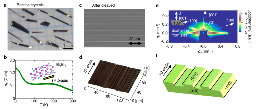
Figure 2a shows a photographic image of Bi4Br4 crystals we used for experiments. XRD measurements have confirmed a bilayer structure in the crystal (Supplementary Note 3). A semiconducting property is observed in the overall behavior of electrical resistivity (Fig. 2b). Significantly, however, we find a saturation toward the lowest temperature, implying that topological edge-states contribute to the electrical conduction. Cleaved surfaces were investigated by scanning electron microscopy (SEM) and laser microscopy (Figs. 2c and 2d, respectively). A number of terraces and facets were observed to be aligned parallel to the chain direction (the -axis in Fig. 1b). These have been revealed to be composed of the (001) and (100) crystal planes by grazing-incidence small-angle X-ray-scattering (GISAXS) measurements (Fig. 2e and Supplementary Note 4), which exhibits two reflection lines separated by , same as the edge angle in the unit cell (see Fig. 1b). A huge number of crystal hinges, therefore, should be naturally exposed on a cleaved surface (Fig. 2f). The local conductivity maps obtained by microwave impedance microscopy (MIM) [26] also show signatures of conductive hinge states in exfoliated flakes of Bi4Br4 (Supplementary Note 5). This unique situation gives us a great opportunity to directly observe the topological hinge states by ARPES with a photon beam of 50 m in size.
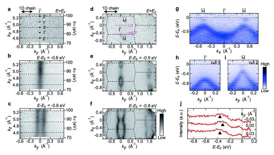
We have performed synchrotron-based ARPES measurements on the cleaved surface of Bi4Br4 and observed a semiconducting band structure consistent with DFT band calculations (Supplementary Note 6). Figures 3a-c plot the ARPES intensities at different binding energies measured along a - sheet around the point; corresponds to the chain direction, and were swept by changing photon energies (s). While there are no states observed at (Fig. 3a), line-like structures appear at the energies lower than eV (Figs. 3b and c). The 1D dispersions indicate that the interlayer coupling of chains along the -axis is negligible (Supplementary Note 7). The electronic states along a - sheet have also been measured at eV (Fig. 3d-f). While the photoelectron intensities are weak, island-like intensities are seen around at (Fig. 3d). At higher binding energies (Figs. 3e and 3f), highly anisotropic structures appear, indicating that the band disperses weakly in the direction perpendicular to the chain (or direction). These features are more directly revealed in Figs. 3g-i, by plotting the ARPES dispersion along -- (Fig. 3g) and along across (Fig. 3h) and (Fig. 3i). The valence band maximum is located about eV as examined in Fig. 3j, where energy distribution curves (EDCs) close to are extracted from Fig. 3i. The weak intensities near , yielding islands around in Fig. 3d, mostly comes from spectral tails of the unoccupied conduction band in bulk, which may be shifted down to lower binding energies by the effect of surface band bending. While the overall band shape is similar to that of -Bi4I4 [14], the semiconducting gap in Bi4Br4 ( eV) is more than two times larger (Supplementary Note 8). These results agree with our DFT calculations, which expect that the band gap calculated with SOC is larger in Bi4Br4 than -Bi4I4 (see Figs. 1g and h). Since the band structure is very simple and the band gap is relatively large for topological insulators, Bi4Br4 is an ideal candidate for the first demonstration of a HOTI state.
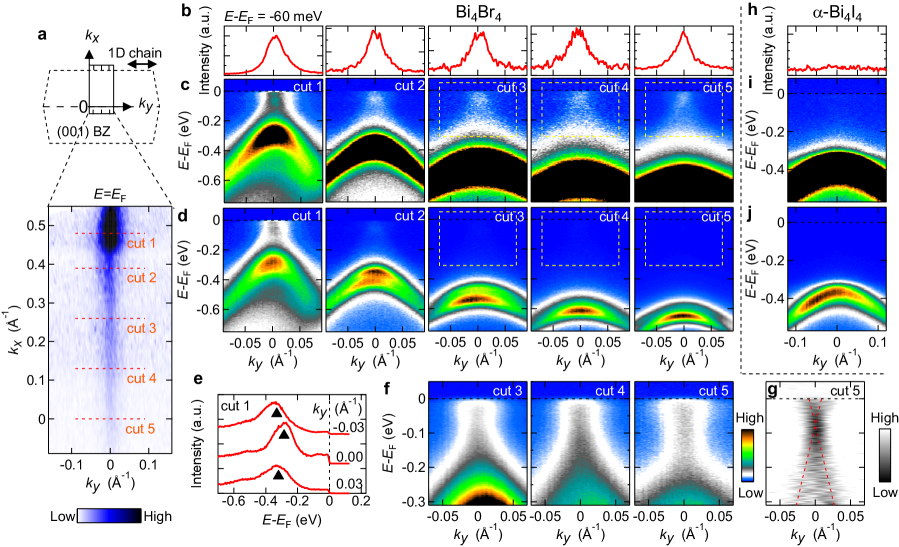
Here we provide evidence for the topological hinge states in Bi4Br4 obtained by a laser-based ARPES that has many advantages to investigate topological states, owing to its high energy- and momentum-resolution and high efficiency of data acquisition [27]. Figure 4a plots the ARPES intensities at covering a rectangle region in the upper panel; relatively weak signals are clearly seen by selecting a proper color scale. Island-like intensities around originate from the spectral tails, as argued above. More importantly, our high-quality data clearly exhibit intensities with a 1D distribution along the line at . In Fig. 4d, we plot ARPES dispersions obtained along several momentum cuts (orange dashed lines in Fig. 4a). The hole-like bands approach at , and disperse toward higher binding energies as moving away from . Detailed properties around are examined in Fig. 4e by extracting EDCs; these have a good agreement with those of the bulk bands observed by synchrotron-based ARPES, showing the band gap () of eV and finite intensities at due to the spectral tails of the unoccupied conduction band. We have also more directly estimated the value of eV by the experiment with the K-deposition technique on the sample surface, which brings the conduction bands down below (see supplementary Fig. S8).
Most interestingly, we found metallic in-gap states with Dirac-like dispersions for all the momentum cuts, as clearly visible by changing the color scale (Fig. 4c); the 1D Fermi surface in Fig. 4a is, thus, formed by these dispersions. The in-gap states are also confirmed in the momentum distribution curves (MDCs) at the roughly estimated Dirac point ( meV) (Fig. 4b). Magnified ARPES images (marked by yellow boxes in Figs. 4c and 4d) with higher statistics (Fig. 4f) and a curvature plot for one of these (Fig. 4g) [28] visualize the Dirac band inside the bulk band gap. These observations are in sharp contrast to the case for a trivial insulator -Bi4I4 (Figs. 4h-j): there is no indication for in-gap states in the image (Fig. 4j) even after changing the color scale (Fig. 4i), nor in MCD at meV (Fig. 4h). The Dirac band we observed in Bi4Br4, therefore, is attributed to the topological state. This result is especially intriguing in that the difference in chain-stacking is the origin of the different band topologies between Bi4Br4 and -Bi4I4. The experimentally determined ( eV) of Bi4Br4 is much larger than the bilayer splitting ( eV), avoiding a rare situation that BVBs and BCBs are mixed only subtly. Therefore, the 1D Dirac-band we observed should be due to a topological hinge state, and thus Bi4Br4 is a HOTI.
The noble concept of the topological material-design we have provided will open up a new pathway to materials science. In particular, the Bi4Br4 verified to be the first higher-order topological insulator provides various advantages in application, owing to its unique crystal structure built from the van der Waals stacking of bismuth bromide chains; since a bunch of crystal hinges are exposed on this crystal, a large amount of topological edge-current could be generated. In bismuth halides, multiple topological phases can be selected by different procedures of chain-stacking, which offers the capability of designing and engineering novel functional materials by thin film growth and microfabrication. Notably, the 1D nanowires obtained by simple exfoliation technique may play a crucial role in developing the devices for Majorana-based topological computing by transferring the nanowires onto a superconducting substrate [29, 30].
References
- [1] Cao, Y. et al. Correlated Insulator Behaviour at Half-Filling in Magic Angle Graphene Superlattices. Nature 556, 80–84 (2018). URL http://www.nature.com/articles/nature26154.
- [2] Cao, Y. et al. Unconventional superconductivity in magic-angle graphene superlattices. Nature 556, 43–50 (2018). URL http://www.nature.com/articles/nature26160.
- [3] Tran, K. et al. Evidence for moiré excitons in van der Waals heterostructures. Nature 567, 71–75 (2019). URL http://www.nature.com/articles/s41586-019-0975-z.
- [4] Alexeev, E. M. et al. Resonantly hybridized excitons in moiré superlattices in van der Waals heterostructures. Nature 567, 81–86 (2019). URL http://www.nature.com/articles/s41586-019-0986-9.
- [5] Seyler, K. L. et al. Signatures of moiré-trapped valley excitons in MoSe2/WSe2 heterobilayers. Nature 567, 66–70 (2019). URL http://www.nature.com/articles/s41586-019-0957-1.
- [6] Jin, C. et al. Observation of moiré excitons in WSe2/WS2 heterostructure superlattices. Nature 567, 76–80 (2019). URL http://www.nature.com/articles/s41586-019-0976-y.
- [7] von Benda, H., Simon, A. & Bauhofer, W. Zur Kenntnis von BiBr und BiBr1,167. Z. Anorg. Allg. Chem. 438, 53–67 (1978). URL http://doi.wiley.com/10.1002/zaac.19784380105.
- [8] Filatova, T. et al. Electronic structure, galvanomagnetic and magnetic properties of the bismuth subhalides Bi4I4 and Bi4Br4. J. Solid State Chem. 180, 1103–1109 (2007). URL http://linkinghub.elsevier.com/retrieve/pii/S0022459607000278.
- [9] Zhou, J.-J., Feng, W., Liu, C.-C., Guan, S. & Yao, Y. Large-Gap Quantum Spin Hall Insulator in Single Layer Bismuth Monobromide Bi4Br4. Nano Lett. 14, 4767–4771 (2014). URL https://pubs.acs.org/doi/10.1021/nl501907g.
- [10] Li, X. et al. Pressure-induced phase transitions and superconductivity in a quasi–1-dimensional topological crystalline insulator -Bi4Br4. Proc. Natl. Acad. Sci. 116, 17696–17700 (2019). URL http://www.pnas.org/lookup/doi/10.1073/pnas.1909276116.
- [11] Tang, F., Po, H. C., Vishwanath, A. & Wan, X. Efficient topological materials discovery using symmetry indicators. Nat. Phys. 15, 470–476 (2019). URL http://www.nature.com/articles/s41567-019-0418-7.
- [12] Hsu, C.-H. et al. Purely rotational symmetry-protected topological crystalline insulator -Bi4Br4. 2D Mater. 6, 031004 (2019). URL https://iopscience.iop.org/article/10.1088/2053-1583/ab1607.
- [13] Rasche, B. et al. Stacked topological insulator built from bismuth-based graphene sheet analogues. Nat. Mater. 12, 422–425 (2013). URL http://www.nature.com/doifinder/10.1038/nmat3570.
- [14] Noguchi, R. et al. A weak topological insulator state in quasi-one-dimensional bismuth iodide. Nature 566, 518–522 (2019). URL http://www.nature.com/articles/s41586-019-0927-7.
- [15] Khalaf, E. Higher-order topological insulators and superconductors protected by inversion symmetry. Phys. Rev. B 97, 205136 (2018). URL https://link.aps.org/doi/10.1103/PhysRevB.97.205136.
- [16] Matsugatani, A. & Watanabe, H. Connecting higher-order topological insulators to lower-dimensional topological insulators. Phys. Rev. B 98, 205129 (2018). URL https://link.aps.org/doi/10.1103/PhysRevB.98.205129.
- [17] Po, H. C., Vishwanath, A. & Watanabe, H. Symmetry-based indicators of band topology in the 230 space groups. Nat. Commun. 8, 50 (2017). URL http://www.nature.com/articles/s41467-017-00133-2.
- [18] Song, Z., Zhang, T., Fang, Z. & Fang, C. Quantitative mappings between symmetry and topology in solids. Nat. Commun. 9, 3530 (2018). URL http://www.nature.com/articles/s41467-018-06010-w.
- [19] Zhang, T. et al. Catalogue of topological electronic materials. Nature 566, 475–479 (2019). URL http://www.nature.com/articles/s41586-019-0944-6.
- [20] Vergniory, M. G. et al. A complete catalogue of high-quality topological materials. Nature 566, 480–485 (2019). URL http://www.nature.com/articles/s41586-019-0954-4.
- [21] Tang, F., Po, H. C., Vishwanath, A. & Wan, X. Comprehensive search for topological materials using symmetry indicators. Nature 566, 486–489 (2019). URL http://www.nature.com/articles/s41586-019-0937-5.
- [22] Khalaf, E., Po, H. C., Vishwanath, A. & Watanabe, H. Symmetry Indicators and Anomalous Surface States of Topological Crystalline Insulators. Phys. Rev. X 8, 031070 (2018). URL https://link.aps.org/doi/10.1103/PhysRevX.8.031070.
- [23] Schindler, F. et al. Higher-order topology in bismuth. Nat. Phys. 14, 918–924 (2018). URL http://www.nature.com/articles/s41567-018-0224-7.
- [24] Fang, C. & Fu, L. New classes of topological crystalline insulators having surface rotation anomaly. Sci. Adv. 5, eaat2374 (2019). URL http://advances.sciencemag.org/lookup/doi/10.1126/sciadv.aat2374.
- [25] Zhang, T. et al. Topological crystalline insulators with rotation anomaly. Phys. Rev. Res. 1, 012001 (2019). URL https://link.aps.org/doi/10.1103/PhysRevResearch.1.012001.
- [26] Lai, K., Kundhikanjana, W., Kelly, M. & Shen, Z. X. Modeling and characterization of a cantilever-based near-field scanning microwave impedance microscope. Rev. Sci. Instrum. 79, 063703 (2008). URL http://aip.scitation.org/doi/10.1063/1.2949109.
- [27] Lv, B., Qian, T. & Ding, H. Angle-resolved photoemission spectroscopy and its application to topological materials. Nat. Rev. Phys. 1, 609–626 (2019). URL http://www.nature.com/articles/s42254-019-0088-5.
- [28] Zhang, P. et al. A precise method for visualizing dispersive features in image plots. Rev. Sci. Instrum. 82, 043712 (2011). URL http://aip.scitation.org/doi/10.1063/1.3585113.
- [29] Hsu, C.-H., Stano, P., Klinovaja, J. & Loss, D. Majorana Kramers Pairs in Higher-Order Topological Insulators. Phys. Rev. Lett. 121, 196801 (2018). URL https://link.aps.org/doi/10.1103/PhysRevLett.121.196801.
- [30] Jäck, B. et al. Observation of a Majorana zero mode in a topologically protected edge channel. Science 364, 1255–1259 (2019). URL http://www.sciencemag.org/lookup/doi/10.1126/science.aax1444.
Data availability
The data that support the findings of this study are available from the corresponding author on reasonable request.
Acknowledgements
We thank D. Hamane for SEM characterization of the sample surface. We also thank X. Ma and D. Abeysinghe for their support in the exfoliation of Bi4Br4 samples. The work done at Tokyo Institute of Technology was supported by a CREST project [JPMJCR16F2] from Japan Science and Technology Agency (JST). The GISAXS experiments were performed under the approval of PF-PAC No. 2018G661. We thank Diamond Light Source for access to beamline I05 under proposal SI20445 that contributed to the results presented here. Use of the Stanford Synchrotron Radiation Light source, SLAC National Accelerator Laboratory, is supported by the U.S. Department of Energy, Office of Science, Office of Basic Energy Sciences under Contract No. DE-AC02-76SF00515. The MIM work was supported by the United States Army Research Office under Grant No. W911NF-17-1-0542. R.N. acknowledges support by JSPS under KAKENHI Grant No.18J21892 and support by JSPS through the Program for Leading Graduate Schools (ALPS).
Author Contribution
T.Ko. and T.Sa. planned the experimental project.
R.N. conducted ARPES experiments and analyzed the data.
Ke.K, P.Z., C.L., C.B., S.Sa., H.T., S.K., Ki.K.,K.Y., A.H., V.K., A.G., A.B., T.Ki., C.C., M.H., D.L., S.Sh., and T.Ko. supported ARPES experiment.
R.N., Z.J., Z.X., D.L. and K.L. performed MIM experiments and analyzed the data.
M.K., T.T. and T.Sa. made and characterized Bi4Br4 single crystals and
performed transport experiments. R.N. and M.K. took laser-microscope images. T.Sh. performed GISAXS experiment. R.N. measured SEM image.
T.Sa., M.H., M.O. and R.A. calculated the band structure and analyzed the band topology.
R.N., Z.J., Ke.K., M.H., M.O., T.Sh., K.L., T.Sa. and T.K. wrote the paper.
All authors discussed the results and commented on the manuscript.
Author Information
The authors declare no competing financial interests. Correspondence and requests for materials should be addressed to T.Sa (email: sasagawa@msl.titech.ac.jp) or T.K. (email: kondo1215@issp.u-tokyo.ac.jp).
METHODS
Samples.
Following a similar procedure as described in [14], single crystals of Bi4Br4 were grown by the chemical vapor transport method. The transport agent used was HgBr, and the optimized temperatures were 285 ∘C and 188 ∘C for the source and growth zones, respectively. The electrical resistivity of Bi4Br4 single crystals was measured by a standard four-probe technique using the Quantum Design Physical Property Measurement System (PPMS).
DFT calculations.
First, we performed the structural optimization using the Perdew-Burke-Ernzerhof (PBE) parametrization of the generalized gradient approximation (GGA) [1], and the projector augmented wave method [2] with the inclusion of the spin-orbit coupling as implemented in Vienna ab initio Simulation Package [3, 4, 5, 6].
In the structural optimization, we optimized atomic coordinates using the experimental lattice parameters as reported in [14] for -Bi4I4 and shown in Fig. S3 for Bi4Br4.
Next, we performed first-principles band-structure calculation using the Becke-Johnson potential [7] as implemented in the WIEN2k code [8]. The muffin-tin radii for all atoms were set to 2.5 a.u. and the maximum modulus for the reciprocal lattice vectors was chosen so that . We took a 18183 -mesh. From the calculated band structures, we extracted the Wannier functions of the Bi- and Br(I)- orbitals using the Wien2Wannier and Wannier90 codes [9, 10, 11, 12]. We did not perform the maximal localization procedure for the Wannier functions to prevent orbital mixing among the different spin components. In the nanowire calculations for Bi4Br4 and -Bi4I4, we set 125 and 126 wires, respectively, which have the same symmetry as each bulk crystal, and used the Wannier function, where we stacked the 12 wires along the -axis and 5 and 6 wires along the -axis. In the 125 Bi4Br4 wires, the two surfaces perpendicular to the -axis are the A-layers in Fig.1.
GISAXS measurements.
GISAXS experiments were performed at the beamline 3A of the Photon Factory at KEK. The x-ray energy was 11 keV, and the slit-cut beam size was 0.1 0.1 mm. The glancing angle of the x-ray was 0.1∘ with respect to the Bi4Br4 (001) plane. The scattered x-rays were detected with PILATUS-100K located 1 m downstream of the sample. For the alignment of sample orientation, the 001 and 200 Bragg reflections were used. All the measurements were performed at room temperature.
ARPES set-up.
Standard-ARPES measurement with synchrotron radiation was performed at the HR-ARPES branch of the beamline I05 of the Diamond Light Source equipped with a ScientaOmicron R4000 analyzer and beamline 5-2 of Stanford Synchrotron Radiation Lightsource (SSRL) equipped with a ScientaOmicron DA30L analyzer. The sample temperature was fixed at 10 K during the measurements. The photon energy was set at between 70 and 100 eV. The angular resolution was 0.1∘ and the overall energy resolution was better than 20 meV.
Laser-based ARPES measurements were performed at the Institute for Solid State Physics, The University of Tokyo [13].
The laser system provides 6.994-eV photons [14].
The measurement temperature of the samples was about 20 K. The angle resolution was 0.3∘ and the overall energy resolution was set to less than 5 meV.
Synchrotron-based nano-ARPES measurements presented in Supplementary Note 7 were performed at the 3.2L-Spectromicroscopy beamline of the Elettra Light Source [15]. A Schwarzschild objective was used to focus the photon beam to a spot of less than 1 m in size. The photoelectron detector is facility-made, and it is rotatable inside the measurement chamber, which also enables Fermi surface mapping without sample rotation. The photon energy was set at 74 eV, and the sample temperature was kept at around 20 K. The overall energy resolutions were set to be better than 60 meV. ARPES data were analyzed using the inverse mapping functions described in [16].
MIM measurements and sample preparations. The MIM work presented in Supplementary Note 5 was performed on a commercial AFM platform (ParkAFM XE-70). Shielded cantilever probes from PrimeNano Inc. were used. Bi4Br4 thin flakes used in MIM experiments were first mechanically exfoliated onto polypropylene carbonate (PPC)-coated polydimethylsiloxane (PDMS) stamps using Scotch tape. The flakes were then transferred onto SiO2 (300 nm)/Si substrates and immediately moved to the measurement systems.
References
- [1] Perdew, J. P., Burke, K. & Ernzerhof, M. Generalized gradient approximation made simple. Phys. Rev. Lett. 77, 3865-3868 (1996). https://link.aps.org/doi/10.1103/PhysRevLett.77.3865.
- [2] Kresse, G. & Joubert, D. From ultrasoft pseudopotentials to the projector augmented-wave method. Phys. Rev. B 59, 1758-1775 (1999). https://link.aps.org/doi/10.1103/PhysRevB.59.1758.
- [3] Kresse, G. & Hafner, J. Ab initio molecular dynamics for liquid metals. Phys. Rev. B 47, 558-561 (1993). https://link.aps.org/doi/10.1103/PhysRevB.47.558.
- [4] Kresse, G. & Hafner, J. Ab initio molecular-dynamics simulation of the liquid-metal-amorphous-semiconductor transition in germanium. Phys. Rev. B 49, 14251-14269 (1994). https://link.aps.org/doi/10.1103/PhysRevB.49.14251.
- [5] Kresse, G. & Furthmüller, J. Efficiency of ab-initio total energy calculations for metals and semiconductors using a plane-wave basis set. Comput. Mater. Sci. 6, 15-50 (1996). https://linkinghub.elsevier.com/retrieve/pii/0927025696000080.
- [6] Kresse, G. & Furthmüller, J. Efficient iterative schemes for ab initio total-energy calculations using a plane-wave basis set. Phys. Rev. B 54, 11169-11186 (1996). https://link.aps.org/doi/10.1103/PhysRevB.54.11169.
- [7] Becke, A. D. & Johnson, E. R. A simple effective potential for exchange. J. Chem. Phys. 124, 221101 (2006). http://aip.scitation.org/doi/10.1063/1.2213970.
- [8] Blaha, P. Schwarz, K. Madsen, G. K. H. Kvasnicka, D. Luitz, J. Laskowski, R. Tran, F. & Marks, L. D. WIEN2k, An Augmented Plane Wave + Local Orbitals Program for Calculating Crystal Properties (Karlheinz Schwarz, Techn. Universität Wien, Austria, 2018). ISBN 3-9501031-1-2.
- [9] Marzari, N. & Vanderbilt, D. Maximally localized generalized Wannier functions for composite energy bands. Phys. Rev. B 56, 12847-12865 (1997). https://link.aps.org/doi/10.1103/PhysRevB.56.12847.
- [10] Souza, I., Marzari, N. & Vanderbilt, D. Maximally localized Wannier functions for entangled energy bands. Phys. Rev. B 65, 035109 (2001). https://link.aps.org/doi/10.1103/PhysRevB.65.035109.
- [11] Kunes̆, J. et al. Wien2wannier: From linearized augmented plane waves to maximally localized Wannier functions. Comput. Phys. Commun. 181, 1888-1895 (2010). https://linkinghub.elsevier.com/retrieve/pii/S0010465510002948.
- [12] Pizzi, G. et al., Wannier90 as a community code: new features and applications. J. Phys. Cond. Matt. 32, 165902 (2020) https://iopscience.iop.org/article/10.1088/1361-648X/ab51ff/pdf.
- [13] Yaji, K. et al. High-resolution three-dimensional spin- and angle-resolved photoelectron spectrometer using vacuum ultraviolet laser light. Rev. Sci. Instrum. 87, 53111 (2016). http://aip.scitation.org/doi/10.1063/1.4948738.
- [14] Shimojima, T., Okazaki, K. and Shin, S. Low-Temperature and High-Energy-Resolution Laser Photoemission Spectroscopy. J. Phys. Soc. Japan 84, 72001 (2015). http://journals.jps.jp/doi/10.7566/JPSJ.84.072001.
- [15] Dudin, P. et al. Angle-resolved photoemission spectroscopy and imaging with a submicrometre probe at the SPECTROMICROSCOPY-3.2L beamline of Elettra. J. Synchrotron Radiat. 17, 445-450 (2010). https://doi.org/10.1107/S0909049510013993.
- [16] Ishida, Y. & Shin, S. Functions to map photoelectron distributions in a variety of setups in angle-resolved photoemission spectroscopy. Rev. Sci. Instrum. 89, 043903 (2018). http://aip.scitation.org/doi/10.1063/1.5007226.