Exceptional coupling in extreme skin-depth waveguides
for extremely low waveguide crosstalk
Photonic chips can miniaturize complicate optical systems very tiny and portable, providing versatile functionalities for many optical applications marin2017microresonator ; atabaki2018integrating ; dutt2018chip ; sun2013large ; miller2020large ; kim2018photonic ; hummon2018photonic ; mehta2016integrated ; spencer2018optical ; kim2017dispersion ; cheben2018subwavelength ; li2017controlling ; wang2019chip ; halir2015waveguide . Increasing the photonic chip integration density is highly desired as it provides more functionalities, low cost, and lower power consumption oulton2008hybrid ; kim2015mode ; haffner2015all ; kim2014polarization ; song2015high ; gatdula2019guiding ; shen2015metamaterial ; shen2016increasing ; gabrielli2012chip ; Jahani2018ControllingIntegration . However, photonic chip integration density is limited by the waveguide crosstalk, which is caused by the evanescent waves in the cladding. Here we show that the waveguide crosstalk can be suppressed completely with the exceptional coupling in extreme skin-depth (eskid) waveguides. The anisotropic dielectric perturbations in the coupled eskid waveguides cause such an exceptional coupling, resulting in infinitely long coupling length. We demonstrate the extreme suppression of waveguide crosstalk via exceptional coupling on a silicon-on-insulator (SOI) platform, which is compatible with a complementary metal–oxide–semiconductor (CMOS) process. The idea of exceptional coupling in eskid waveguides can be applied to many other photonic devices as well, significantly reducing entire chip footprints.
The waveguide crosstalk is the power transfer of a light signal between the adjacent waveguides due to the evanescent waves. In a typical photonic chip, to avoid the crosstalk, waveguides need to be separated large enough and this limits the integration density of photonic chips. To overcome this limit, plasmonics have been explored with their ability to confine light in subwavelength scale oulton2008hybrid ; kim2015mode ; kim2014polarization ; haffner2015all ; however, there exist metallic losses to consider. Topological approaches that use a waveguide super-lattice song2015high ; gatdula2019guiding , inverse design shen2015metamaterial ; shen2016increasing , or transformations optics gabrielli2012chip have been proposed, yet these approaches add more complexity or phase variations in the design, and often lead to higher scattering losses. Recently, an extreme skin-depth (e-skid) waveguide that utilizes all-dielectric metamaterial claddings has been proposed to reduce the crosstalk Jahani2018ControllingIntegration . The subwavelength multilayers effectively work as an anisotropic metamaterial and suppress the evanescent waves in the cladding. This reduces the crosstalk and an approximately 30 times longer coupling length has been demonstrated compared to typical strip waveguides. However, even with the reduced skin-depth, there still is some degree of crosstalk, and the further question remains as to if it is possible to suppress the crosstalk completely.
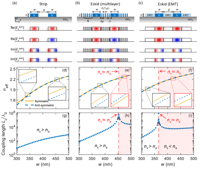
To push the limit of chip integration density, we explore the exceptional coupling phenomena in the eskid waveguides by evaluating coupling lengths of the three different coupled waveguide schemes. Figures 1(a-c) show the cross-sections and geometric parameters of the three coupled waveguide configurations: (a) typical strip waveguides, (b) practical eskid waveguides with subwavelength-scale multilayer claddings, and (c) ideal eskid waveguides with anisotropic metamaterial claddings using the effective medium theory (EMT). All configurations are implemented on an SOI platform, i.e., Si and SiO2 as a core and a substrate, respectively. Throughout the paper, we explore the coupled modes between the two identical fundamental quasi-transverse-electric (quasi-TE0) modes, and the electric field profiles and of the coupled symmetric (sym) and anti-symmetric (anti) modes are also plotted in Figs.1(a-c). The multilayer eskid in Fig. 1(b) is a practical structure that can be fabricated with the current electron-beam lithography Jahani2018ControllingIntegration and CMOS technology orcutt2011nanophotonic ; stojanovic2018monolithic . The EMT eskid in Fig. 1(c) is an equivalent model with an anisotropic metamaterial, and its permittivities ( and ) follow milton2002theory ; jahani2014transparent ; Jahani2018ControllingIntegration ,
| (1a) | ||||
| (1b) | ||||
where, and are the permittivities of Si and air, respectively. is the filling fraction of Si. Note that, due to the large index contrast between Si and air, a huge anisotropy can appear and its anisotropy can be engineered by controlling the . With the increased anisotropy, the skin-depth in the cladding can be reduced, lowering the crosstalk jahani2014transparent ; Jahani2018ControllingIntegration .
The crosstalk between the two adjacent waveguides is assessed by the coupling length , which quantifies the length that transfers the optical power completely from one waveguide to the other waveguide; i.e., the crosstalk is lower for a longer , and it’s the opposite for a shorter . To compare the coupling lengths of each configuration, effective refractive indices of the coupled symmetric (, yellow solid) and anti-symmetric (, blue dashed) modes are simulated in Figs. 1(d-f), and their corresponding normalized coupling lengths (blue dots) are plotted in Figs. 1(g-i): (d,g) strip, (e,h) eskid with multilayer, and (f,i) eskid with EMT. Each coupling length is normalized by the free-space wavelength at nm and the of the two identical waveguides can be calculated by yariv2006photonics ; huang1994coupled
| (2) |
where, is the magnitude of the index difference between and . The inset boxes in Figs. 1(d-f) show the zoomed-in view of and at different regimes. Notice that, in the coupled eskids of Figs. 1(e,f), there are non-trivial coupling regimes where (red-shaded region). This non-trivial coupling is not observable in typical strip waveguides (Fig. 1(d)). More importantly, at the transition from a typical coupling regime () to the non-trivial coupling regime (), there is an exceptional coupling where approaches zero (i.e., ). As shown in Figs. 1(h,i), at these exceptional coupling points, the coupling length approaches to infinity, i.e., the crosstalk is suppressed completely. For multilayer and EMT cases, the exceptional couplings appear at different . This is due to the deviations of effective and of the multilayer compared to those of ideal EMT (see Supplementary).
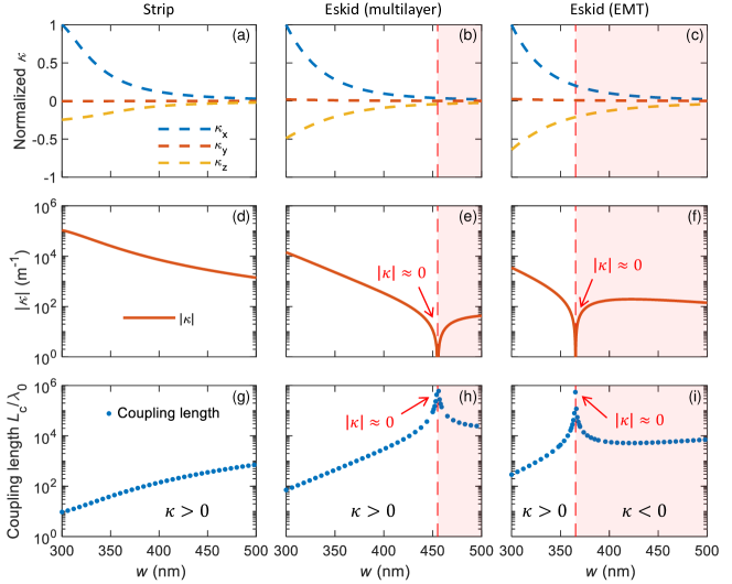
To understand the underlying mechanism of the exceptional coupling, we analyzed each configuration using the anisotropic coupled mode analysis. In a quasi-TE0, an component is dominant but there is an component as well. Thus, to address the coupled modes correctly, the anisotropic coupling coefficients from all the field components (i.e., , and ) should be considered(see Methods). The overall coupling coefficient can be obtained by adding each component together (i.e., ) and the coupling length of the two same waveguides is the following yariv2006photonics ; huang1994coupled :
| (3) |
Figures 2(a-c) show the normalized coupling coefficients of each component (blue dashed), (orange dashed), and (yellow dashed), and their corresponding overall coupling coefficient (orange solid) and the normalized coupling length (blue dots) are plotted in Figs. 2(d-f) and Figs. 2(g-i), respectively: (a,d,g) coupled strip, and coupled eskid with (b,e,h) the multilayer and (c,f,i) EMT. In every case, as the increases, the coupling coefficients are reduced and the coupling lengths are increased, due to the higher confinement in the core and less overlap between the modes. In Fig. 2(a), the is clearly dominant than the other components, even with a non-negligible . The sign of is negative due to the imaginary , and it counteracts with the in determining the . In coupled strip waveguides, the magnitude of is always greater than that of (i.e., ) as the is dominant in the quasi-TE0 mode. Figure 2(d) shows the overall with the actual unit, and its corresponding normalized coupling length in Fig. 2(g) exactly matches the result from the full numerical simulation in Fig. 1(g).
In cases of eskids, there are non-trivial coupling regimes, where the magnitude of is greater than that of (i.e., ) as shown in Figs. 2(b) and 2(c) (red-shaded). These non-trivial coupling regimes in the coupled eskids are due to the anisotropic dielectric perturbations of the scheme (i.e., ), allowing the to compensate for the . The overall approaches to zero at the transition points, resulting in infinitely long coupling lengths (i.e., ) as in Figs. 2(h) and 2(i); these results also match well with the full simulation results in Figs. 1(h) and 1(i), respectively.
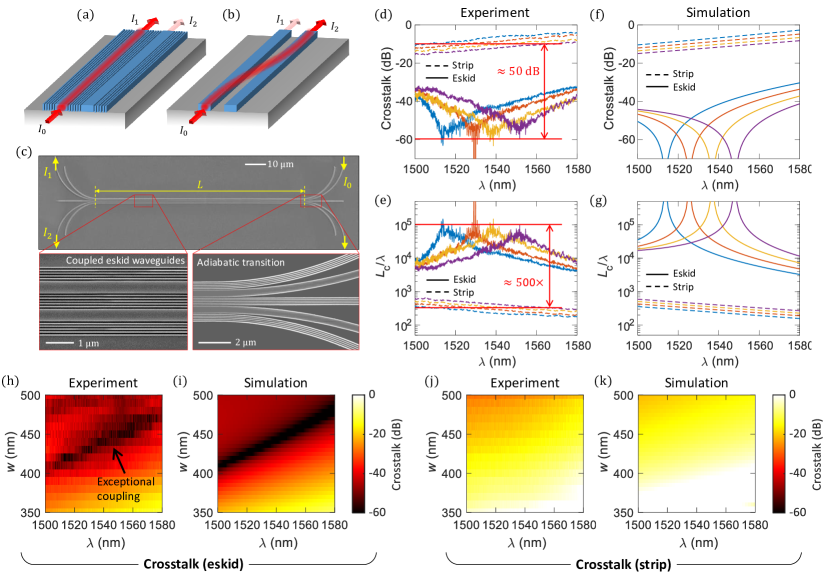
To confirm our theoretical finding, we fabricated the coupled eskid (multilayer) and strip waveguides, and the crosstalks of each configuration are measured and compared. Figures 3(a) and 3(b) show the schematic views of the coupled eskid and strip waveguides, respectively, and Fig. 3(c) shows the SEM images of the fabricated devices. The indicates the optical power at the input port, and the and are the output powers at the through and coupled ports, respectively. The crosstalk is defined as the power ratio and it is related to the coupling length , following yariv2006photonics ,
| (4) |
where is the physical length of the coupled waveguides. To measure the crosstalk, we sent a light signal to the input port through a fiber-coupled grating coupler, then output signals and were measured simultaneously (see Methods). Figure 3(d) shows the experimentally measured crosstalk (in dB) and Fig. 3(e) is the corresponding normalized coupling length. Solid and dashed lines are the cases of the coupled eskid and strip waveguides, respectively, and each color represents different core widths . Figures 3(f) and 3(g) are the simulation results that correspond to Figs. 3(d) and 3(e), respectively. Note that the dips in the crosstalk and the peaks in the indicate the exceptional couplings. In Fig. 3(d), notice that the crosstalks of the coupled eskids are suppressed down to about dB, which is approximately 50 dB lower than that of the standard strip waveguides. As to the coupling length, the peak of the coupled eskids are in the order of , which is approximately times longer than the case of strip waveguides. As shown in Figs. 3(f) and 3(g), in an ideal case of exceptional coupling, the crosstalk can be suppressed completely with an infinitely long coupling length. However, in real experiments, the minimum crosstalk is limited by the scattering from the waveguide sidewall roughness and the cross-coupling at the transition between strip to eskid waveguides(see Supplementary). Still, the crosstalk that we achieved here is extremely low, and, to the best of our knowledge, these results demonstrate the longest coupling length, spanning about of free-space wavelengths.
The full map plots of the crosstalk, as functions of and , for the coupled eskid and strip waveguides are plotted in Figs. 3(h,i) and 3(h,i), respectively, clearly showing much lower crosstalk with the eskid waveguides. Figures 3(h,j) and 3(i,k) are the experimental and simulation results, respectively. The dark regions in Figs. 3(h,i) indicate the exceptional coupling, which can be observed only with the coupled eskid waveguides. Since the exceptional coupling occurs at the point where the coupling coefficient compensates the , the exceptional coupling can be engineered by controlling the modal overlaps between the two waveguides. For example, as shown in Figs. 3(h,i), increasing the shifts the exceptional coupling to a longer wavelength; this is because a wider increases the light confinement and reduces the modal overlap between the two coupled eskids, while a longer wavelength works the opposite way. Similarly, changing the other geometric parameters and shifts the exceptional coupling point, and we also observed exceptional couplings with different numbers of eskid layers and filling fraction (see Supplementary).
In summary, we have presented exceptional couplings in the coupled eskid waveguides that can achieve extremely low waveguide crosstalk. Our coupled mode analysis reveals that the unique anisotropic dielectric perturbation of the eskid is the fundamental origin of the non-trivial coupling regime that can cause the exceptional coupling at the transition. We experimentally demonstrated the exceptional couplings on an SOI platform, which is low-loss, low-cost, and compatible with the CMOS foundry. We suppressed the crosstalk approximately 50 dB lower than the case of strip waveguides, which corresponds to an approximately 500 times longer coupling length. The exceptional coupling can be engineered with geometric parameters and the filling fraction of the eskids. Our approach of using the exceptional coupling in the coupled eskid waveguides drastically increase the photonic chip integration density and can be applied to other photonic devices realizing highly dense PICs.
Methods
Numerical simulation.
A commercially available software (Lumerical Mode Solution) was used to calculate the effective refractive indices of the coupled symmetric and anti-symmetric modes. For the implementation of an ideal metamaterial cladding, the EMT was used for the and , following Eq. (1).
For the strip-to-eskid adiabatic transition, a full 3D FDTD simulation was used to minimize the cross-coupling efficiency (see Supplementary).
Coupled mode analysis. For the coupled mode analysis in Fig. 2, we calculated the , following yariv2006photonics ; huang1994coupled :
| (5) |
where the subscript and . and are the normalized electric fields of isolated quasi-TE0 modes at each side and is the dielectric perturbation between them. Note that, for isotropic media, as in strip waveguides, all the dielectric perturbation components are the same (i.e., ); however, for anisotropic cases, as in eskid waveguides, they are different (i.e., ), causing the non-trivial coupling regime. Each coupling coefficient was added together to form the total coupling coefficient , and Eq. (3) was used to calculate the corresponding coupling length.
Device fabrication.
The photonic chips were fabricated on an SOI wafer ( nm thick Si on a m SiO2) using the JEOL JBX-6300 EBL system, which operated at KeV energy, pA beam current,
and m m exposure field. A solvent rinse was done, followed by min of O2 plasma treatment. Hydrogen silsequioxane resist (HSQ, Dow-Corning XR-1541-006) was spin coated at rpm and pre-exposure baked on a hotplate at for min. Shape placements by the machine grid, the beam stepping grid, and the spacing between dwell points during shot shape writing were nm, nm, and nm, respectively. An exposure dose of was used. The resist was developed in tetramethylammonium hydroxide (TMAH) for min followed by a flowing deionized waster rinse for s and an isopropanol rinse for s. Then, nitrogen was blown to air dry. After development of the resist, the unexposed top silicon layer was etched by a Cl2/O2 in a reactive ion-plasma etching tool (Trion Minilock) to transfer the pattern from the resist to the silicon layer.
Device characterization. The photonic chips were characterized by a custom-built grating coupler setup. An angle polished () eight-channel fiber array was used to couple light in and out of the grating couplers. The fiber array was mounted on a five-axis stage with a high-precision adjuster with 20 nm sensitivity in XYZ direction. A Keysight Tunable Laser 81608A was used as the source and a Keysight N7744A optical power meter with InGaAs sensors was used as the output detector. The wavelength was swept from 1500 to 1580 nm with a step of 100 pm. A polarization controller was used to control the polarization of the input laser light.
Acknowledgements.
This material is based upon work supported by the National Science Foundation under Grant No. ECCS-1930784. This work was performed, in part, at the Center for Integrated Nanotechnologies, an Office of Science User Facility operated for the U.S. Department of Energy (DOE) Office of Science by Los Alamos National Laboratory (Contract 89233218CNA000001) and Sandia National Laboratories (Contract DE-NA-0003525).Author contributions
S.K. conceived the project and guided the theoretical and experimental investigations. M.M. conducted all the numerical simulations and the coupled mode analysis. S.A. measured all the devices. I.A. fabricated all devices used in the reported experiments. Y.L. and M.Q. supported the project with initial sets of devices. M.M. and S.K. wrote the manuscript. All discussed and commented on the results.
References
- (1) Marin-Palomo, P. et al. Microresonator-based solitons for massively parallel coherent optical communications. Nature 546, 274–279 (2017).
- (2) Atabaki, A. H. et al. Integrating photonics with silicon nanoelectronics for the next generation of systems on a chip. Nature 556, 349–354 (2018).
- (3) Dutt, A. et al. On-chip dual-comb source for spectroscopy. Sci. Adv. 4, e1701858 (2018).
- (4) Sun, J., Timurdogan, E., Yaacobi, A., Hosseini, E. S. & Watts, M. R. Large-scale nanophotonic phased array. Nature 493, 195 (2013).
- (5) Miller, S. A. et al. Large-scale optical phased array using a low-power multi-pass silicon photonic platform. Optica 7, 3–6 (2020).
- (6) Kim, S. et al. Photonic waveguide to free-space gaussian beam extreme mode converter. Light Sci. Appl. 7, 72 (2018).
- (7) Hummon, M. et al. Photonic chip for laser stabilization to an atomic vapor at a precision of . Optica 5, 2334 (2018).
- (8) Mehta, K. K. et al. Integrated optical addressing of an ion qubit. Nat. Nanotech. 11, 1066–1070 (2016).
- (9) Spencer, D. et al. An optical-frequency synthesizer using integrated photonics. Nature 557, 81–85 (2018).
- (10) Kim, S. et al. Dispersion engineering and frequency comb generation in thin silicon nitride concentric microresonators. Nat. Commun. 8, 372 (2017).
- (11) Cheben, P., Halir, R., Schmid, J. H., Atwater, H. A. & Smith, D. R. Subwavelength integrated photonics. Nature 560, 565–572 (2018).
- (12) Li, Z. et al. Controlling propagation and coupling of waveguide modes using phase-gradient metasurfaces. Nat. Nanotechnol. 12, 675 (2017).
- (13) Wang, Z. et al. On-chip wavefront shaping with dielectric metasurface. Nat. Commun. 10, 1–7 (2019).
- (14) Halir, R. et al. Waveguide sub-wavelength structures: a review of principles and applications. Laser Photonics Rev. 9, 25–49 (2015).
- (15) Oulton, R. F., Sorger, V. J., Genov, D., Pile, D. & Zhang, X. A hybrid plasmonic waveguide for subwavelength confinement and long-range propagation. Nat. Photon. 2, 496 (2008).
- (16) Kim, S. & Qi, M. Mode-evolution-based polarization rotation and coupling between silicon and hybrid plasmonic waveguides. Sci. Rep. 5, 18378 (2015).
- (17) Haffner, C. et al. All-plasmonic mach–zehnder modulator enabling optical high-speed communication at the microscale. Nat. Photon. 9, 525–528 (2015).
- (18) Kim, S. & Qi, M. Polarization rotation and coupling between silicon waveguide and hybrid plasmonic waveguide. Opt. Express 23, 9968–9978 (2015).
- (19) Song, W. et al. High-density waveguide superlattices with low crosstalk. Nat. Commun. 6, 7027 (2015).
- (20) Gatdula, R., Abbaslou, S., Lu, M., Stein, A. & Jiang, W. Guiding light in bent waveguide superlattices with low crosstalk. Optica 6, 585–591 (2019).
- (21) Shen, B., Polson, R. & Menon, R. Metamaterial-waveguide bends with effective bend radius . Opt. Lett. 40, 5750–5753 (2015).
- (22) Shen, B., Polson, R. & Menon, R. Increasing the density of passive photonic-integrated circuits via nanophotonic cloaking. Nat. Commun. 7, 13126 (2016).
- (23) Gabrielli, L. H., Liu, D., Johnson, S. G. & Lipson, M. On-chip transformation optics for multimode waveguide bends. Nat. Commun. 3, 1217 (2012).
- (24) Jahani, S. et al. Controlling evanescent waves using silicon photonic all-dielectric metamaterials for dense integration. Nat. Commun. 9, 1893 (2018).
- (25) Orcutt, J. S. et al. Nanophotonic integration in state-of-the-art cmos foundries. Opt. Express 19, 2335–2346 (2011).
- (26) Stojanović, V. et al. Monolithic silicon-photonic platforms in state-of-the-art CMOS SOI processes. Opt. Express 26, 13106–13121 (2018).
- (27) Milton, G. W. The theory of composites (Cambridge University Press, 2002).
- (28) Jahani, S. & Jacob, Z. Transparent subdiffraction optics: nanoscale light confinement without metal. Optica 1, 96–100 (2014).
- (29) Yariv, A. & Yeh, P. Photonics: optical electronics in modern communications (Oxford University Press, 2006).
- (30) Huang, W.-P. Coupled-mode theory for optical waveguides: an overview. J. Opt. Soc. Am. A 11, 963–983 (1994).