Microscopic origin of molecule excitation via inelastic electron scattering in scanning tunneling microscope
Abstract
The scanning-tunneling-microscope-induced luminescence emerges recently as an incisive tool to measure the molecular properties down to the single-molecule level. The rapid experimental progress is far ahead of the theoretical effort to understand the observed phenomena. Such incompetence leads to a significant difficulty in quantitatively assigning the observed feature of the fluorescence spectrum to the structure and dynamics of a single molecule. This letter is devoted to reveal the microscopic origin of the molecular excitation via inelastic scattering of the tunneling electrons in scanning tunneling microscope. The current theory explains the observed large photon counting asymmetry between the molecular luminescence intensity at positive and negative bias voltage.
Introduction – The physical limitation of conventional semiconductor devices spurs the recent development of single molecule photoelectronics (Aradhya and Venkataraman, 2013; Xin et al., 2019; Sun et al., 2014), where the incisive tool to probe single molecular structure and dynamics is of great demand. Combining the high resolution of scattering tunneling microscope (STM) with the specificity of fluorescence spectroscopy of molecules, STM-induced luminescence (STML) provides an ideal tool to study the photon emission and dynamics on the single-molecule level (Flaxer et al., 1993; Berndt et al., 1993). Experimental breakthroughs have allowed direct observations of the single-molecular properties, e.g., the dipole-dipole coupling between molecules (Zhang et al., 2016; Doppagne et al., 2017; Luo et al., 2019), the energy transfer in molecular dimers (Imada et al., 2016), and the Fano-like lineshape (Imada et al., 2017; Zhang et al., 2017; Kröger et al., 2018). Yet, the retarded theoretical followup prevents us from conclusively understanding the single-molecular properties through the quantitative analyses of experimental data.
Such lag of the corresponding theoretical effort has led to inconsistent between experimental explanations. The underlying origin of the asymmetric emission intensity at positive and negative bias between the tip and substrate was assigned as the carrier-injection mechanism in (Zhang et al., 2016), while it was also understood as inelastic electron tunneling (probably mediated by the localized surface plasmon) (Doppagne et al., 2018) for the same molecule, i.e., the single ZnPc molecule. The question exists even on the asymmetry with larger tunneling current at positive bias or versa (Zhang et al., 2016; Doppagne et al., 2018). The inconsistency remains unresolved mainly due to the lack of microscopic theory to conclusively determine the properties of the different tunneling mechanisms, which are mixed in the ab initio calculations (Wu et al., 2019; Miwa et al., 2019a).
In this letter, we reveal the underlying microscopic origin of the inelastic electron scattering down to the basic Coulomb interaction between the tunneling electron and the single molecule. Our theory shows the asymmetry with larger tunneling current and photon counting rate at negative bias, in turn, excludes the possibility of the opposite asymmetry to be attributed to the inelastic electron scattering. Such attempt shall initiate the understanding of the experimental feature from its microscopic origin and stimulate the theoretical studies of the STML.
Model – For the clarity of the notation, we sketch the design of the single-molecule STML in Fig. 1(a). A molecule, simplified for clarity as a dipole with positive (red) and negative (blue) charge, is deposited on a salt-covered metal substrate. A metal tip is positioned above the substrate plane. Both the tip and substrate are typically used with noble meta, e.g., silver (Ag). With nonzero bias voltage, an electron (black) from one electrode excites the molecule via the Coulomb interaction during its tunneling through the vacuum and then enters into the other electrode (see Fig. 1(b)). Subsequently, the excited molecule emits a photon by the spontaneous emission, which is measured by the photon counting to reveal molecular properties.
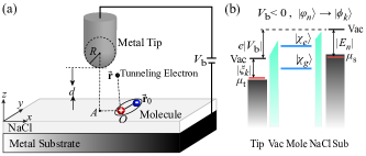
The Hamiltonian for the setup is divided into three parts as , where is the Hamiltonian for the tunneling electron between the tip and substrate, is the Hamiltonian of the molecule, and is the interaction between the tunneling electron and the single molecule. The Hamiltonian of the tunneling electron is , where is the potential for the tunneling electron at position and is the mass of an electron. The wave functions are written for different regions (Bardeen, 1961; Gottlieb and Wesoloski, 2006) as
| (1a) | ||||
| (1b) | ||||
where () is the Hamiltonian of the free tip (substrate) obtained by neglecting the potential in the substrate (tip) region. is the eigenstate of free tip (substrate) with where is the eigenenergy with zero bias voltage. The detailed form of the wave functions are discussed in the supplementary material. The Hamiltonian for the molecule is simplified as a two-level system (Nian et al., 2018; Nian and Lü, 2019) , where is its excited (ground) state with energy .
The key element to understand the mechanism is the interaction between the molecule and the tunneling electron. For the purpose of clarity, we consider a simple case of one tunneling electron. The interaction, simplified from the Coulomb interaction, resembles the dipole interaction as
| (2) |
where denotes the effective electric dipole moment of the molecule. is the effective charge number, and stands for the vector of the center of the electrons in molecule. represents the vector of the tunneling electron. Here, we have chosen the central position of the positive charge of molecule as the origin of the coordinate system. The detailed derivation can be found for the molecule with multiple chemical bonds (Minkin et al., 1970) in the supplementary material.
The interaction is rewritten explicitly with the basis of the wave functions of the single molecule and tunneling electron as
| (3) |
We have defined the transition matrix element from substrate’s state to tip’s state and from tip’s state to substrate’s state . is the transition matrix between molecular ground and excited states. The electron-dipole interaction in Eq. (3) will induce energy transfer between the tunneling electron and the molecule (the state of the two-level molecule is flipped).
Tip’s wave function in the vacuum region has the asymptotic spherical form where is the position of tip’s center of curvature and is its decay factor. The normalized coefficient can be determined by first-principles calculations. This wave function is typical known as the s-wave, which is the simplest case for the tip (Bardeen, 1961; Chen, 1990). Contribution from other wave functions can be similarly considered as that in the studies of STM (Chen, 1990). And substrate’s wave function decays along the direction with decay factor (Tersoff and Hamann, 1983, 1985) and the normalization constant . With the wave functions for the tip and substrate, the transition matrix element is explicitly written as
| (4) |
where is the component of the molecular dipole moment. And without loss of generality, we have chosen the position of tip’s center of curvature along axis, i.e., . By taking the decay wave functions of tip and substrate into account, we integrate over the region between plane and as an approximation. And in the later discussion, we ignore the dependence of on the normalization constants and by taking them to independent on the index and .
Asymmetry of photon counting – To understand the asymmetry of photon counting, we calculate the tunneling rate at negative bias (), illustrated in Fig. 1(b), where the Fermi level of tip is lower than that of substrate. The molecule is initially in its ground state and the tunneling electron in one of substrate’s eigenstate, i.e., . To the first order of and , we obtain the time evolution of the system as
| (5) |
where the second and third terms stand for elastic and inelastic tunneling respectively. In order to obtain the above result, we have applied the rotating-wave approximation for Hamiltonian in Eq. (3). The corresponding tunneling amplitudes read
| (6) | ||||
| (7) |
where is the transition matrix element of the elastic tunneling and is the optical gap of the single molecule.
We will focus on the inelastic tunneling process instead of the elastic tunneling which has been well explored in the earlier development (Bardeen, 1961; Tersoff and Hamann, 1983, 1985; Chen, 1990) of STM. The inelastic tunneling rate from to is . The overall inelastic electron current at negative voltage is explicitly rewritten as
| (8) |
where () are the density of state of tip (substrate) at the energy . is the Fermi-Dirac distribution of electrons in tip or substrate state at energy , chemical potential , and temperature . rules out all the tunneling processes whose energy do not conserve. Without loss of generality, we consider here the tip and substrate are of the same metal (Ag).
In STML experiment, the temperature of the ultrahigh-vacuum chamber is low enough, typically lower than 10K (Chen et al., 2019; Zhang et al., 2016; Imada et al., 2016; Miwa et al., 2019b; Doppagne et al., 2018; Luo et al., 2019; Imada et al., 2017; Zhang et al., 2017; Doppagne et al., 2017; Kröger et al., 2018), that the Fermi-Dirac distribution function is approximately a Heaviside function, i.e., for and for . The inelastic tunneling current becomes
| (9) |
Eq. (9) suggests that the current for inelastic tunneling is nonzero only at the condition for the negative bias case.
For the positive bias , the current for the inelastic tunneling is obtained with the similar method as
| (10) |
Similar to the negative bias case, the condition for a nonzero inelastic current is . The equal bias voltage for nonzero inelastic current at negative and positive bias is an important feature different from the carrier-injection mechanism where the electron injection requires different voltage for the negative and positive bias (Zhang et al., 2016; Chong, 2016). With Eqs. (9 and 10), we obtain the inelastic tunneling current as
| (11) |
Photon counting of molecular fluorescence is a quantity relevant for probing the properties of the single molecule. Once excited, the molecule will decay to its lower state spontaneously with rate . The photon counting rate is proportional to the inelastic current
| (12) |
The detailed derivation can be found in the supplementary materials. In Fig. 2, we plot the photon counting rate as the function of the bias voltage between the tip and the substrate. The blue solid and black dashed lines show the relative emission intensity for tip’s center of curvature and , respectively. The Fermi energy of silver is eV, and the density of state of silver can be found in (Papaconstantopoulos, 2015). Without loss of generality, we choose the tip right above the molecule () and the molecular dipole along the direction ( while ). The distance between tip and molecule is nm. As predicted in Eq. (11), the bias voltages for nonzero inelastic current at negative and positive bias are the same, i.e., eV. Insets in Fig. 2 describe the mechanism of the inelastic electron scattering.
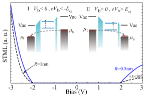
Another important feature is the asymmetry of the larger photon counting at negative bias than that at positive bias, as illustrated in Fig. 2. This intensity asymmetry stems from the eigenfunction asymmetry of tip and substrate. The tip’s wave function decays spherically with factor , and substrate’s wave function decays along the direction with factor . The relation between the elements of the transition matrix at positive bias and that at negative bias reads
| (13) |
The ratio between the transition matrix element at positive bias and that at negative bias is . Inserting Eq. (13) into Eq. (9), we obtain the ratio of the emission intensity as (see Supplementary Material for details)
| (14) |
The current equation shows the characteristic asymmetry with larger current at negative bias induced by inelastic electron tunneling. Such asymmetry for inelastic scattering is caused by geometry shape of the tip and the substrate, and persists with different materials.
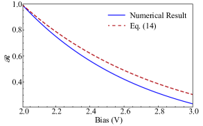
In Fig. 3, we show the dependence of the asymmetrical ratio as a function of the bias voltage with both the analytical formula (red dashed line) in Eq. (14) and the numerical result (blue solid line) calculated with the exact tunneling rate from Eqs. (9-10). The analytical formula shows an agreement on the trend that the asymmetry of the photon counting increases with increasing bias voltage. The exponential decay of the ratio as function of bias voltage is predicted in Eq. (14) and shall be tested with the experimental data.
With the theoretical predictions above, we revisit the important features observed in recent experiments (Zhang et al., 2016; Doppagne et al., 2018; Kröger et al., 2018). In the single-hydrocarbon fluorescence induced by STM (Kröger et al., 2018), the phenomenon that the emission intensity at positive bias was lower than that at negative bias is in line with our prediction. Though such the asymmetric intensity feature (the intensity at positive bias was much lower than that at negative bias) of a single ZnPc molecule was attributed to the carrier-injection mechanism (Zhang et al., 2016), we emphasis that the inelastic electron scattering mechanism may also play an important role in this feature. By changing the tip and substrate material from Ag to Au, Doppagne el al. (Doppagne et al., 2018) observed a phenomenon which was opposite to the feature in (Zhang et al., 2016). The emission of a single neutral ZnPc molecule at positive bias was 30 times more intense than that at negative bias. Our theory definitely excludes the inelastic electron scattering mechanism as the origin of such asymmetric luminescence in (Doppagne et al., 2018).
In conclusion, we have derived the microscopic origin of the molecular excitation via the inelastic electron scattering mechanism in single-molecule STML. By the model, we obtain the emission intensity in the inelastic electron scattering mechanism. We find that inelastic electron scattering mechanism requires a symmetric bias voltage for nonzero inelastic current which equals the optical gap of this two-level molecule exactly. It implies that the energy window between the Fermi levels of two electrodes should at least equal the optical gap of the molecule (Chong, 2016). Importantly, we reveal an asymmetric emission intensity at negative and positive bias which is due to the asymmetric forms of wave functions at two electrodes and show that the ratio of such asymmetry decays with tip’s radius of curvature and bias voltage. Our model offers us a theoretical insight into the molecular excitation in the inelastic electron scattering process which has never been explored before.
Before closing, it is worthy to mention that the inelastic scattering mechanism is one of the three mechanisms proposed now and the photon counting obtained here is one part of the total emission intensity. Further research is needed for elucidating the competition of these three mechanisms and finding the dominant one under certain conditions.
Acknowledgements.
H. D. thanks Yang Zhang for the helpful discussion. This work is supported by the NSFC (Grants No. 11534002 and No. 11875049), the NSAF (Grant No. U1730449 and No. U1530401), and the National Basic Research Program of China (Grants No. 2016YFA0301201 and No. 2014CB921403). H.D. also thanks The Recruitment Program of Global Youth Experts of China.References
- Aradhya and Venkataraman (2013) S. V. Aradhya and L. Venkataraman, Nat. Nanotechnol. 8, 399 (2013).
- Xin et al. (2019) N. Xin, J. Guan, C. Zhou, X. Chen, C. Gu, Y. Li, M. A. Ratner, A. Nitzan, J. F. Stoddart, and X. Guo, Nat. Rev. Phys. 1, 211 (2019).
- Sun et al. (2014) L. L. Sun, Y. A. Diaz-Fernandez, T. A. Gschneidtner, F. Westerlund, S. Lara-Avila, and K. Moth-Poulsen, Chem. Soc. Rev. 43, 7378 (2014).
- Flaxer et al. (1993) E. Flaxer, O. Sneh, and O. Cheshnovsky, Science 262, 2012 (1993).
- Berndt et al. (1993) R. Berndt, R. Gaisch, J. K. Gimzewski, B. Reihi, R. R. Schlittler, W. D. Schneider, and M. Tschudy, Science 262, 1425 (1993).
- Zhang et al. (2016) Y. Zhang, Y. Luo, Y. Zhang, Y. J. Yu, Y. M. Kuang, L. Zhang, Q. S. Meng, Y. Luo, J. L. Yang, Z. C. Dong, and J. G. Hou, Nature (London) 531, 623 (2016).
- Doppagne et al. (2017) B. Doppagne, M. C. Chong, E. Lorchat, S. Berciaud, M. Romeo, H. Bulou, A. Boeglin, F. Scheurer, and G. Schull, Phys. Rev. Lett. 118, 127401 (2017).
- Luo et al. (2019) Y. Luo, G. Chen, Y. Zhang, L. Zhang, Y. J. Yu, F. F. Kong, X. J. Tian, Y. Zhang, C. X. Shan, Y. Luo, J. L. Yang, V. Sandoghdar, Z. C. Dong, and J. G. Hou, Phys. Rev. Lett. 122, 233901 (2019).
- Imada et al. (2016) H. Imada, K. Miwa, M. Imai-Imada, S. Kawahara, K. Kimura, and Y. Kim, Nature (London) 538, 364 (2016).
- Imada et al. (2017) H. Imada, K. Miwa, M. Imai-Imada, S. Kawahara, K. Kimura, and Y. Kim, Phys. Rev. Lett. 119, 013901 (2017).
- Zhang et al. (2017) Y. Zhang, Q. S. Meng, L. Zhang, Y. Luo, Y. J. Yu, B. Yang, Y. Zhang, R. Esteban, J. Aizpurua, Y. Luo, J. L. Yang, Z. C. Dong, and J. G. Hou, Nat. Commun. 8, 15225 (2017).
- Kröger et al. (2018) J. Kröger, B. Doppagne, F. Scheurer, and G. Schull, Nano Lett. 18, 3407 (2018).
- Doppagne et al. (2018) B. Doppagne, M. C. Chong, H. Bulou, A. Boeglin, F. Scheurer, and G. Schull, Science 361, 251 (2018).
- Wu et al. (2019) X. Y. Wu, R. L. Wang, Y. Zhang, B. W. Song, and C. Y. Yam, J. Phys. Chem. C 123, 15761 (2019).
- Miwa et al. (2019a) K. Miwa, H. Imada, M. Imai-Imada, K. Kimura, M. Galperin, and Y. Kim, Nano Lett. 19, 2803 (2019a).
- Bardeen (1961) J. Bardeen, Phys. Rev. Lett. 6, 57 (1961).
- Gottlieb and Wesoloski (2006) A. D. Gottlieb and L. Wesoloski, Nanotechnology 17, R57 (2006).
- Nian et al. (2018) L. L. Nian, Y. Wang, and J. T. Lü, Nano Lett. 18, 6826 (2018).
- Nian and Lü (2019) L. L. Nian and J. T. Lü, J. Phys. Chem. C 123, 18508 (2019).
- Minkin et al. (1970) V. I. Minkin, O. A. Osipov, and Y. A. Zhdanov, DIPOLE MOMENTS IN ORGANIC CHEMISTRY, 1st ed., edited by W. E. Vaughan (Plenum Press, New York, 1970) pp. 79.
- Chen (1990) C. J. Chen, Phys. Rev. B 42, 8841 (1990).
- Tersoff and Hamann (1983) J. Tersoff and D. R. Hamann, Phys. Rev. Lett. 50, 1998 (1983).
- Tersoff and Hamann (1985) J. Tersoff and D. R. Hamann, Phys. Rev. B 31, 805 (1985).
- Chen et al. (2019) G. Chen, Y. Luo, H. Y. Gao, J. Jiang, Y. J. Yu, L. Zhang, Y. Zhang, X. G. Li, Z. Y. Zhang, and Z. C. Dong, Phys. Rev. Lett. 122, 177401 (2019).
- Miwa et al. (2019b) K. Miwa, H. Imada, M. Imai-Imada, S. Kawahara, J. Takeya, M. Kawai, M. Galperin, and Y. Kim, Nature (London) 570, 210 (2019b).
- Chong (2016) M. C. Chong, Electrically driven fluorescence of single molecule junctions, Ph.D. thesis, Université de Strasbourg, France (2016).
- Papaconstantopoulos (2015) D. A. Papaconstantopoulos, Handbook of the band structure of elemental solids: from Z = 1 to Z = 112, 2nd ed. (Springer, New York, 2015) pp. 243.