Nonlinear optical study of commensurability effects in graphene-hBN heterostructures
Abstract
Second-order nonlinear optical response allows to detect different properties of the system associated with the inversion symmetry breaking. Here, we use a second harmonic generation effect to investigate the alignment of a graphene/hexagonal Boron Nitride heterostructure. To achieve that, we activate a commensurate-incommensurate phase transition by a thermal annealing of the sample. We find that this structural change in the system can be directly observed through a strong modification of a nonlinear optical signal. This result reveals the potential of a second harmonic generation technique for probing structural properties of layered systems.
Two-dimensional (2D) materials attract a lot of attention due to their remarkable characteristics. These systems have a rich variety of structural modifications and chemical compositions, which results in a high tunability of their physical properties. Moreover, collective many-body effects that are essentially strong in two dimensions give rise to nontrivial phases of matter, which appear promising for various electronic and opto-electronic applications. For example, transition metal dichalcogenides (TMDs) reveal competing charge Mulazzi et al. (2010); Sun et al. (2015) and spin-ordered Zhuang and Hennig (2016); Isaacs and Marianetti (2016), as well as Mott insulating Cho et al. (2016); Ma et al. (2016) states in the mono- and multilayered phases. Also, 2D systems show a superconducting behaviour Uchihashi (2016) that was theoretically predicted for black phosphorus Shao et al. (2014); Ge et al. (2015) and antimony Lugovskoi et al. (2019), and experimentally observed in black phosphorus Zhang et al. (2017) and various TMDs Ye et al. (2012); Lu et al. (2015); Xi et al. (2016); Lu et al. (2018).
In a multilayered phase, characteristics of quasi-2D systems depend not only on internal properties of individual layers. Here, the number of layers and, what is even more important, the form of their stacking also plays a significant role. A famous example is a twisted bilayer graphene that at a magic misorientation angle of between two graphene lattices drastically changes electronic properties and becomes superconducting. This remarkable effect has been first theoretically predicted Bistritzer and MacDonald (2011); Suárez Morell et al. (2010) and recently confirmed experimentally Cao et al. (2018a, b); Yankowitz et al. (2019). Also, a strong correlation between the interlayer stacking and optical properties has been reported for MoS2 Hsu et al. (2014); Yin et al. (2014) and hexagonal Boron Nitride (hBN) Kim et al. (2013); Yang et al. (2019).
Recently, it became possible to experimentally produce hybrid systems combining different two-dimensional materials in a layered heterostructure Geim and Grigorieva (2013). This gives even more freedom in designing materials with special characteristics in a controlled way. For heterostructures, the effect of different stacking is much less explored than in the case of multilayered homostructures. However, this issue should also be of a crucial importance as it involves different types of materials. For instance, a change of a misorientation angle between graphene and hBN lattices results in a commensurate-incommensurate phase transition, which strongly affects a crystal symmetry and electronic properties of the system Woods et al. (2014). Therefore, it is very important to have a simple yet sensitive tool that provides the information about the structural properties of a material, because even a small mismatch of different layers dramatically changes characteristics of the system.
Conventional experimental techniques that allow to probe various electronic and symmetry properties of nanostructures are Raman spectroscopy Woods et al. (2014) and transport measurements Gorbachev et al. (2014). Raman technique is by no means a powerful method that, however, requires an accurate interpretation of results, which might not be straightforward even for a simple case of graphene Malard et al. (2009); Ferrari (2007). Also, Raman signals are integrated over rather thick layer of material (500 nm) which may result in additional difficulties during data analysis, as relevant signals might originate from buried layers or interfaces Malard et al. (2009). Transport experiments are much more difficult to perform as they require additional sample preparationtion steps and corresponding facilities. In this regard, an optical second harmonic generation (SHG) is a very promising tool for investigation of different structural properties of 2D materials, being sensitive to the inversion symmetry breaking in the system and, therefore, crucially depends on the number of layers, stacking, alignment and etc. Thus, the SHG has already been used for description of non-centrosymmetric 2D systems, such as MoS2 Li et al. (2013); Hsu et al. (2014); Säynätjoki et al. (2017); Malard et al. (2013); Kumar et al. (2013); Yin et al. (2014) and WS2 Janisch et al. (2014); Seyler et al. (2015); Rosa et al. (2018). Also, the optical SHG response has been observed from graphene, where the inversion symmetry was broken by a presence of an electric field Bykov et al. (2012); Brun and Pedersen (2015).
Experimental SHG studies of quasi-2D homostructures are almost entirely dedicated to mono-, or few-layered systems. An exception is a very recent study where a nonzero SHG response from rather thick hBN (ca. hundred layers) flake has been reported Kim et al. (2019). SHG from layered heterostructures is much less studied, both theoretically Margulis et al. (2013); Vandelli et al. (2019) and experimentally Dean and van Driel (2009, 2010); An et al. (2013), and is mostly focused on graphene/graphite films, where the inversion symmetry is broken by the interface with a substrate.
An effect of the stacking on the nonlinear optical response in layered heterostructures has not been investigated experimentally so far. Here, we address this important question for the cases of mono- and multilayer graphene disposed on an insulating hBN substrate. We show that the change of the SHG response clearly indicates the commensurate-incommensurate phase transition for both considered heterostructures. The change of the alignment in the case of the monolayer graphene has been additionally confirmed by Raman measurements. At the same time, Raman spectroscopy was not able to characterize the structural change in the multilayer graphene/hBN heterostructure. This result suggest that the SHG can be used as a simple and efficient method for probing structural properties and alignment of layered heterostructures.
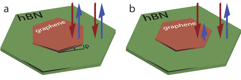
We investigate a nonlinear optical response from graphene flakes placed on top of a hexagonal Boron Nitride (hBN) substrate. In general, a small mismatch between lattice constants of these two materials leads to hexagonal moiré patterns formed in the system Xue et al. (2011); Yankowitz et al. (2012). If a misorientation angle between graphene and hBN lattices is less than , a commensurate stacking is energetically more preferable Woods et al. (2014). In this case, electronic properties of the system can be effectively described by Dirac electrons with a nonzero mass Wallbank et al. (2013); Sachs et al. (2011); Slotman et al. (2015). The latter appears as a result of an inversion symmetry breaking in a graphene/hBN heterostructure. Importantly, the value of the mass varies in space with a period of moiré pattern, but the average value of the mass stays nonzero Bokdam et al. (2014); Sachs et al. (2011); Slotman et al. (2015). Apart from the theoretical prediction, the nonzero average mass in the commensurate phase was also observed in transport experiments Gorbachev et al. (2014). At larger values of the misorientation angle the system undergoes a structural phase transition towards an incommensurate phase Woods et al. (2014). In this phase, the inversion symmetry is still broken locally, but the average value of the mass becomes zero Bokdam et al. (2014). Since a typical focused laser spot is much larger than an interatomic distance, only the average value of the effective mass can be probed in optical experiments. The SHG is known to be very sensitive to the lack of inversion symmetry in the point group of the medium. Therefore, such a nonlinear optical technique a very promising tool for detection of the alignment of such layered heterostructures.
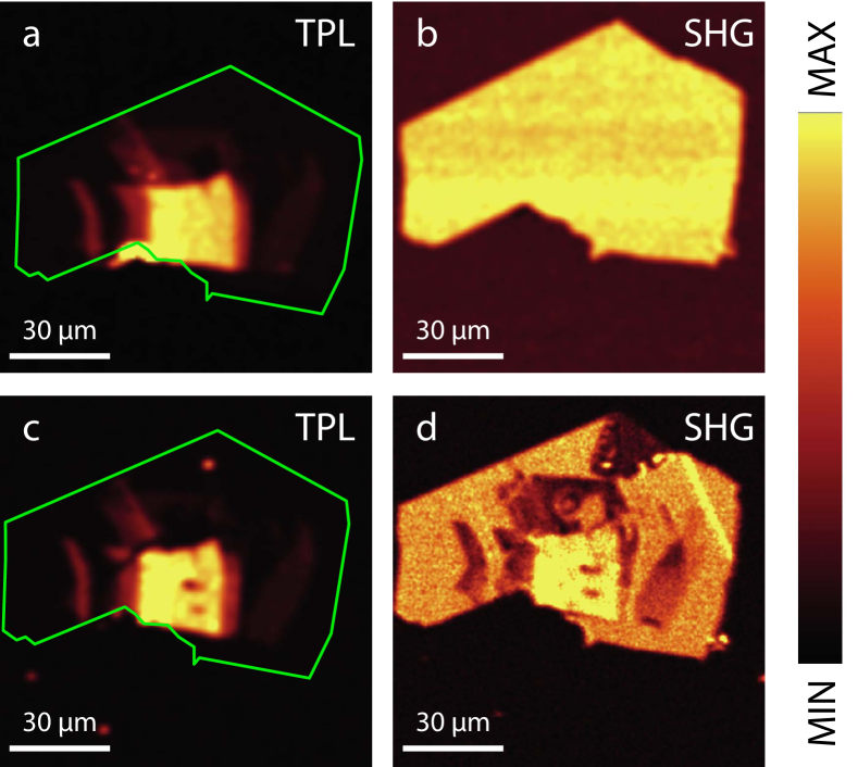
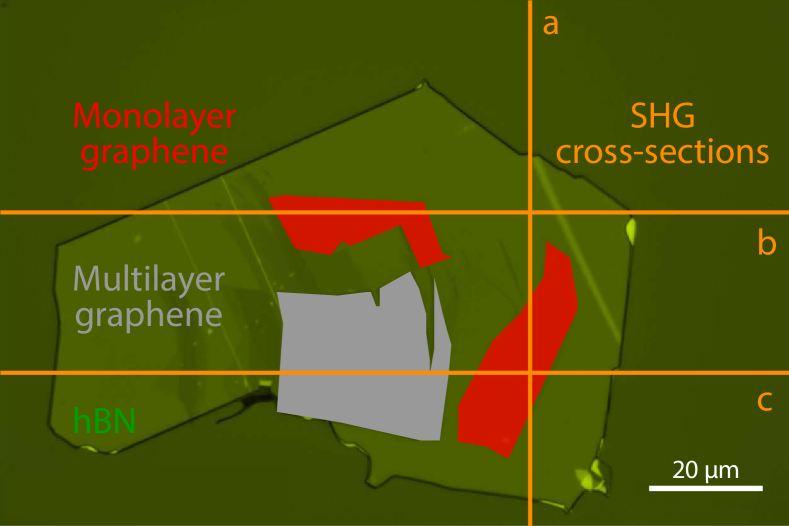
Schematic representation of the experiment is shown in Fig. 1. The optical image of the considered sample obtained from optical microscope through a objective is shown in Fig. 2. Here, red areas highlight single-layer graphene flakes placed on top of the hBN substrate depicted by a light green color. The incommensurate phase for both flakes is confirmed by Raman spectroscopy through the broadening of the 2D-peak in the Raman spectrum Eckmann et al. (2013). A central gray square area corresponds to a multilayer graphene, which alignment with respect to the hBN was not possible to define by Raman measurements. Details of the sample preparation and Raman experiments can be found in the Section “Methods”. A combined optical response has been measured from the sample excited by a 800 nm femtosecond laser. A two-photon luminescence (TPL) signal that was collected at nm is shown in Fig. 3 a. A narrow bandpass filter centered at 400 nm ( 20 nm) was used to detect the SHG signal only (see Fig. 3 b). Description of the experimental set-up can also be found in the Section “Methods”.
Since the TPL is an incoherent process, it is not sensitive to the point group of the medium. Thus, we observe the TPL response only from graphene areas. Here, the strongest signal comes from a multilayer graphene as it has more complex band structure than its single-layer realization. The hBN does not contribute to the TPL, because the corresponding excitation energy eV is lower than the band gap in this material, which is about 6 eV Blase et al. (1995); Cassabois et al. (2016). Thus, a nonzero TPL signal only confirms the presence of graphene flakes on the hBN substrate. As expected, this incoherent optical process is not sensitive to the alignment of the considered heterostructure.
On contrary, the SHG is a coherent process, whose efficiency must obey the symmetry principle Nye et al. (1985). Hence SHG can serve as a probe of symmetries of the point group in the studied medium. For considered materials, the latter is mediated by the value of the average mass (band gap) Vandelli et al. (2019). We observe that the intensity of the SHG response shown in Fig. 3 b is uniform for the entire sample. This fact suggests that there is no inversion symmetry breaking associated with the interaction of graphene with the hBN substrate. Thus, we find that single-layer graphene flakes are not aligned with the hBN, which is consistent with Raman measurements. This result also confirms that the average mass of graphene, which is effectively probed by the SHG, is zero in the incommensurate phase. Importantly, we also do not observe any change of the SHG signal from the multilayer graphene area. This indicates that the multilayer graphene flake is not aligned with hBN substrate as well. As a consequence, the SHG response from the sample is related only to the hBN.
We note that the SHG from a thick hBN is strong. This can be explained by a simple phenomenological model. The SHG arises from the nonlinear polarization induced by an incident laser field . To the leading orders in , this polarization can be written as Heinz (1991):
where the first and second terms describe the electric-dipole and quadrupole contributions to the SHG, respectively. The total SHG response from the system can be divided into the surface and bulk parts. According to Neumann’s principle Nye et al. (1985), the electron-dipole SHG process is allowed only for a non-centrosymmetric medium. This results in a strong second-order optical response from the surface of hBN Vandelli et al. (2019). On contrary, the bulk of hBN obeys the inversion symmetry and contributes to the SHG only through the quadrupole polarization. Although the latter is much smaller than the electric-dipole one, in birefringent materials the total quadrupole contribution from the bulk can be of the same order of magnitude as the surface SHG due to the phase-matching Tom et al. (1983); Heinz (1991). Moreover, in some cases these two processes can hardly be separated from each other Guyot-Sionnest and Shen (1988); Heinz (1991). However, the strength and the relative phase of the quadrupole contribution to the SHG strongly depends on the particular structure of the bulk.
To modify the alignment of the sample, we exploit the finding of the work Woods et al. (2016), where thermal annealing was used to activate the incommensurate-to-commensurate phase transition. For this aim, we induce a local laser heating of the graphene/hBN heterostructure via a long irradiation of the sample. This was done in such a way that the system was under the irradiation for tens of seconds. The estimated energy of the irradiation is 0.06 J/cm2 (the pulse energy is 1.88 nJ, the spot size area is 1 m2). Heated by a laser, the structure relaxed from the incommensurate state to a more favorable commensurate one. After that, a Raman spectroscopy measurement was performed to confirm the phase transition. It has been observed that single-layer graphene flakes became aligned with the underlying hBN forming moiré patterns with the periodicity of 12.5 and 14.0 nm. The alignment of a multilayer graphene has not been determined by Raman spectroscopy. For more details see the SI Stepanov et al. (2020).
Now, we repeat TPL and SHG measurements. Corresponding results are shown in Fig. 3 c and d, respectively. As expected, the TPL signal remains unchanged after the phase transition. This follows from the fact that the electronic band structure of the system at a characteristic energy of nonlinear optical excitations does not change under small rotations Bokdam et al. (2014). On contrary, the SHG response is drastically modified after graphene becomes aligned with the hBN substrate. Indeed, now the SHG intensity picture explicitly shows the position of graphene flakes. According to a theoretical prediction Vandelli et al. (2019), this is a clear signature of the inversion symmetry breaking that occurs due to the interaction of the aligned graphene with the underlying hBN layer. As a consequence, electrons in the commensurate phase of the graphene/hBN heterostructure gain a nonzero average mass Wallbank et al. (2013); Sachs et al. (2011); Slotman et al. (2015); Gorbachev et al. (2014), which is precisely captured by the SHG experiment. Remarkably, we find that the SHG response from the area of the multilayer graphene has also been modified indicating the phase transition towards the commensurate phase.
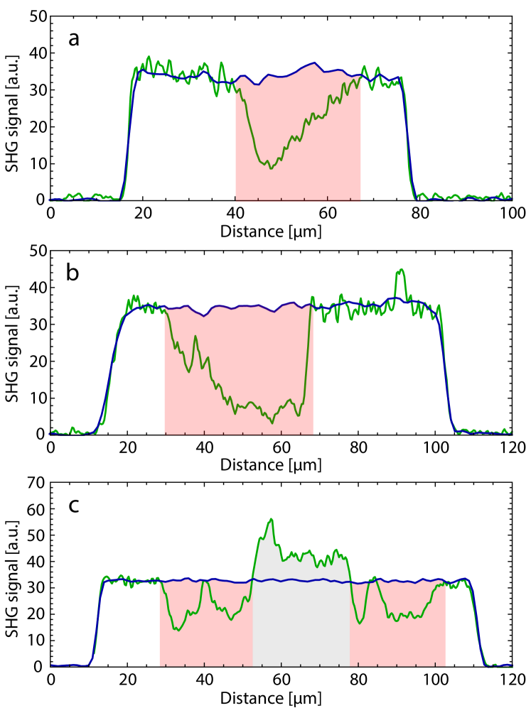
A precise comparison of the normalized intensity of the SHG for different alignments is shown in Fig. 4. Results are obtained for cross-sections along vertical (a) and horizontal (b and c) directions depicted by orange lines in Fig. 2. Blue and green lines in Fig. 4 indicate the SHG signal in the incommensurate and commensurate phases, respectively. Remarkably, we observe a completely different change of the SHG response from single- and multilayer graphene/hBN heterostructures after the phase transition. Indeed, the SHG is suppressed at light red ares that correspond to single-layer graphene flakes. On contrary, the SHG from the aligned multilayer graphene depicted by gray color is enhanced.
It is worth noting that the electric-dipole polarization of the hBN surface has only the imaginary component, because the considered frequency of the light is below the band gap of this material Vandelli et al. (2019). This leads to a phase shift of the corresponding SHG signal with respect to the second-order optical response from the graphene/hBN interface, for which the electric-dipole polarization can have both, real and imaginary components Vandelli et al. (2019). Therefore, the interference between commensurate graphene and underlying hBN can be either destructive or constructive, depending on a particular structure of the system. This fact makes the SHG very appealing for investigation of the inversion symmetry breaking in layered heterostructures, because already the change of the SHG clearly indicates a structural phase transition. In this context, the Raman technique is a less direct method, since it requires additional data processing steps, such as the calculation of the broadening of the 2D peak in the spectrum Eckmann et al. (2013).
For additional confirmation of obtained results, we have performed the TPL and SHG measurements of another aligned single-layer graphene encapsulated between two hBN flakes. In this case, we also observe a strong modification of the SHG signal associated with the presence of the aligned graphene flake between hBN layers. For more details of this experiment please see the SI Stepanov et al. (2020).
In conclusion, we have observed that structural changes in graphene/hBN heterostructures can be explicitly captured using the optical SHG technique. We realized that the incommensurate-to-commensurate phase transition in considered systems can be activated by a local laser heating of the sample. We have found that the SHG method is able to detect the alignment not only of the single-, but also of the multilayer graphene flake disposed on the hBN surface, contrary to Raman spectroscopy. In addition to transport measurements, our nonlinear optical study confirmed that the average mass of electrons in graphene is zero in the incommensurate phase, and is nonzero for the commensurate structure. Our results suggest that the proposed method for detection of the alignment is more direct and, thus, has an advantage over a standard Raman technique.
Methods
Samples for these measurements were fabricated by dry-peel methodology described elsewhere Woods et al. (2014); Kretinin et al. (2014). Control of the alignment is achieved by positioning long, straight edges of the crystals (which tend to be one crystallographic axis, zig-zag or arm-chair) parallel to each other. We use single- and multilayer graphene flakes placed on top of thick hBN ( nm).
Raman spectroscopy measurements were performed using a Horiba Raman spectrometer (grating 1200 GPI) operating with an incident laser at a wavelength of 532 nm and mW power. A confocal microscope was used to focus on the sample through a objective. For more details please see the SI Stepanov et al. (2020).
For nonlinear characterization of the samples WITec alpha300 S confocal microscope was used in reflection geometry. Samples were irradiated by Ti:sapphire oscillator at 800 nm and fs pulse width. Typical laser power was mW before the microscope where about 70% of power reached and were focused on a sample with Zeiss objective. Detected nonlinear response was separated from fundamental wavelength by use of two types of filters. SCHOTT BG39 filter (390-650 nm transmission) was used for experiments when SHG/TPL combined response was detected. Thorlabs FB400-40 filter was used in experiments where only SHG signal was of interest.
Acknowledgements.
Authors thank Chris Berkhout for technical support. Authors also thank Clement Dutreix and Vladimir Kukushkin for fruitful discussions and useful comments. The work of E.A.S. was supported by the Russian Science Foundation, Grant No. 17-72-20041. K.S.N acknowledges support from EU Graphene Flagship Program (contract CNECTICT-604391), European Research Council Synergy Grant Hetero2D, the Royal Society, EPSRC grant EP/N010345/1. The work of M.I.K. was supported by European Research Council via Synergy Grant 854843 - FASTCORR.References
- Mulazzi et al. (2010) M. Mulazzi, A. Chainani, N. Katayama, R. Eguchi, M. Matsunami, H. Ohashi, Y. Senba, M. Nohara, M. Uchida, H. Takagi, and S. Shin, “Absence of nesting in the charge-density-wave system as seen by photoelectron spectroscopy,” Phys. Rev. B 82, 075130 (2010).
- Sun et al. (2015) Xu Sun, Tao Yao, Zhenpeng Hu, Yuqiao Guo, Qinghua Liu, Shiqiang Wei, and Changzheng Wu, “In situ unravelling structural modulation across the charge-density-wave transition in vanadium disulfide,” Phys. Chem. Chem. Phys. 17, 13333–13339 (2015).
- Zhuang and Hennig (2016) Houlong L. Zhuang and Richard G. Hennig, “Stability and magnetism of strongly correlated single-layer ,” Phys. Rev. B 93, 054429 (2016).
- Isaacs and Marianetti (2016) Eric B. Isaacs and Chris A. Marianetti, “Electronic correlations in monolayer ,” Phys. Rev. B 94, 035120 (2016).
- Cho et al. (2016) Doohee Cho, Sangmo Cheon, Ki-Seok Kim, Sung-Hoon Lee, Yong-Heum Cho, Sang-Wook Cheong, and Han Woong Yeom, “Nanoscale manipulation of the Mott insulating state coupled to charge order in 1T-TaS2,” Nature communications 7, 10453 (2016).
- Ma et al. (2016) Liguo Ma, Cun Ye, Yijun Yu, Xiu Fang Lu, Xiaohai Niu, Sejoong Kim, Donglai Feng, David Tománek, Young-Woo Son, Xian Hui Chen, et al., “A metallic mosaic phase and the origin of Mott-insulating state in 1T-TaS2,” Nature communications 7, 10956 (2016).
- Uchihashi (2016) Takashi Uchihashi, “Two-dimensional superconductors with atomic-scale thickness,” Superconductor Science and Technology 30, 013002 (2016).
- Shao et al. (2014) D. F. Shao, W. J. Lu, H. Y. Lv, and Y. P. Sun, “Electron-doped phosphorene: A potential monolayer superconductor,” EPL (Europhysics Letters) 108, 67004 (2014).
- Ge et al. (2015) Yanfeng Ge, Wenhui Wan, Fan Yang, and Yugui Yao, “The strain effect on superconductivity in phosphorene: a first-principles prediction,” New Journal of Physics 17, 035008 (2015).
- Lugovskoi et al. (2019) A. V. Lugovskoi, M. I. Katsnelson, and A. N. Rudenko, “Electron-phonon properties, structural stability, and superconductivity of doped antimonene,” Phys. Rev. B 99, 064513 (2019).
- Zhang et al. (2017) Renyan Zhang, John Waters, Andre K Geim, and Irina V Grigorieva, “Intercalant-independent transition temperature in superconducting black phosphorus,” Nature communications 8, 15036 (2017).
- Ye et al. (2012) J. T. Ye, Y. J. Zhang, R. Akashi, M. S. Bahramy, R. Arita, and Y. Iwasa, “Superconducting dome in a gate-tuned band insulator,” Science 338, 1193–1196 (2012).
- Lu et al. (2015) J. M. Lu, O. Zheliuk, I. Leermakers, N. F. Q. Yuan, U. Zeitler, K. T. Law, and J. T. Ye, “Evidence for two-dimensional Ising superconductivity in gated MoS2,” Science 350, 1353–1357 (2015).
- Xi et al. (2016) Xiaoxiang Xi, Zefang Wang, Weiwei Zhao, Ju-Hyun Park, Kam Tuen Law, Helmuth Berger, László Forró, Jie Shan, and Kin Fai Mak, “Ising pairing in superconducting NbSe2 atomic layers,” Nature Physics 12, 139 (2016).
- Lu et al. (2018) Jianming Lu, Oleksandr Zheliuk, Qihong Chen, Inge Leermakers, Nigel E. Hussey, Uli Zeitler, and Jianting Ye, “Full superconducting dome of strong Ising protection in gated monolayer WS2,” Proceedings of the National Academy of Sciences 115, 3551–3556 (2018).
- Bistritzer and MacDonald (2011) Rafi Bistritzer and Allan H. MacDonald, “Moiré bands in twisted double-layer graphene,” Proceedings of the National Academy of Sciences 108, 12233–12237 (2011).
- Suárez Morell et al. (2010) E. Suárez Morell, J. D. Correa, P. Vargas, M. Pacheco, and Z. Barticevic, “Flat bands in slightly twisted bilayer graphene: Tight-binding calculations,” Phys. Rev. B 82, 121407 (2010).
- Cao et al. (2018a) Yuan Cao, Valla Fatemi, Shiang Fang, Kenji Watanabe, Takashi Taniguchi, Efthimios Kaxiras, and Pablo Jarillo-Herrero, “Unconventional superconductivity in magic-angle graphene superlattices,” Nature 556, 43 (2018a).
- Cao et al. (2018b) Yuan Cao, Valla Fatemi, Ahmet Demir, Shiang Fang, Spencer L Tomarken, Jason Y Luo, Javier D Sanchez-Yamagishi, Kenji Watanabe, Takashi Taniguchi, Efthimios Kaxiras, et al., “Correlated insulator behaviour at half-filling in magic-angle graphene superlattices,” Nature 556, 80 (2018b).
- Yankowitz et al. (2019) Matthew Yankowitz, Shaowen Chen, Hryhoriy Polshyn, Yuxuan Zhang, K. Watanabe, T. Taniguchi, David Graf, Andrea F. Young, and Cory R. Dean, “Tuning superconductivity in twisted bilayer graphene,” Science 363, 1059–1064 (2019).
- Hsu et al. (2014) Wei-Ting Hsu, Zi-Ang Zhao, Lain-Jong Li, Chang-Hsiao Chen, Ming-Hui Chiu, Pi-Shan Chang, Yi-Chia Chou, and Wen-Hao Chang, “Second harmonic generation from artificially stacked transition metal dichalcogenide twisted bilayers,” Acs Nano 8, 2951–2958 (2014).
- Yin et al. (2014) Xiaobo Yin, Ziliang Ye, Daniel A. Chenet, Yu Ye, Kevin O’Brien, James C. Hone, and Xiang Zhang, “Edge Nonlinear Optics on a MoS2 Atomic Monolayer,” Science 344, 488–490 (2014).
- Kim et al. (2013) Cheol-Joo Kim, Lola Brown, Matt W Graham, Robert Hovden, Robin W Havener, Paul L McEuen, David A Muller, and Jiwoong Park, “Stacking order dependent second harmonic generation and topological defects in h-BN bilayers,” Nano letters 13, 5660–5665 (2013).
- Yang et al. (2019) Yaping Yang, Yi-Chao Zou, Colin R Woods, Yanmeng Shi, Jun Yin, Shuigang Xu, Servet Ozdemir, Takashi Taniguchi, Kenji Watanabe, Andre K Geim, et al., “Stacking order in graphite films controlled by van der waals technology,” Nano letters 19, 8526–8532 (2019).
- Geim and Grigorieva (2013) A. K. Geim and I. V. Grigorieva, “Van der Waals heterostructures,” Nature 499, 419–425 (2013).
- Woods et al. (2014) C. R. Woods, L. Britnell, A. Eckmann, R. S. Ma, J. C. Lu, H. M. Guo, X. Lin, G. L. Yu, Y. Cao, R. V. Gorbachev, A. V. Kretinin, J. Park, L. A. Ponomarenko, M. I. Katsnelson, Yu. N. Gornostyrev, K. Watanabe, T. Taniguchi, C. Casiraghi, H-J. Gao, Geim A. K., and K. S. Novoselov, “Commensurate-incommensurate transition in graphene on hexagonal boron nitride,” Nature physics 10, 451 (2014).
- Gorbachev et al. (2014) R. V. Gorbachev, J. C. W. Song, G. L. Yu, A. V. Kretinin, F. Withers, Y. Cao, A. Mishchenko, I. V. Grigorieva, K. S. Novoselov, L. S. Levitov, and A. K. Geim, “Detecting topological currents in graphene superlattices,” Science 346, 448–451 (2014).
- Malard et al. (2009) L. M. Malard, G. Pimenta, M. A.and Dresselhaus, and M. S. Dresselhaus, “Raman spectroscopy in graphene,” Physics Reports 473, 51 – 87 (2009).
- Ferrari (2007) Andrea C. Ferrari, “Raman spectroscopy of graphene and graphite: Disorder, electron–phonon coupling, doping and nonadiabatic effects,” Solid State Communications 143, 47 – 57 (2007), exploring graphene.
- Li et al. (2013) Yilei Li, Yi Rao, Kin Fai Mak, Yumeng You, Shuyuan Wang, Cory R Dean, and Tony F Heinz, “Probing symmetry properties of few-layer MoS2 and h-BN by optical second-harmonic generation,” Nano letters 13, 3329–3333 (2013).
- Säynätjoki et al. (2017) A. Säynätjoki, L. Karvonen, H. Rostami, A. Autere, S. Mehravar, A. Lombardo, R. A. Norwood, T. Hasan, N. Peyghambarian, H. Lipsanen, K. Kieu, A. C. Ferrari, M. Polini, and Sun Z., “Ultra-strong nonlinear optical processes and trigonal warping in MoS2 layers,” Nature Communications 8, 893 (2017).
- Malard et al. (2013) Leandro M. Malard, Thonimar V. Alencar, Ana Paula M. Barboza, Kin Fai Mak, and Ana M. de Paula, “Observation of intense second harmonic generation from MoS2 atomic crystals,” Phys. Rev. B 87, 201401 (2013).
- Kumar et al. (2013) Nardeep Kumar, Sina Najmaei, Qiannan Cui, Frank Ceballos, Pulickel M. Ajayan, Jun Lou, and Hui Zhao, “Second harmonic microscopy of monolayer MoS2,” Phys. Rev. B 87, 161403 (2013).
- Janisch et al. (2014) Corey Janisch, Yuanxi Wang, Ding Ma, Nikhil Mehta, Ana Laura Elías, Néstor Perea-López, Mauricio Terrones, Vincent Crespi, and Zhiwen Liu, “Extraordinary second harmonic generation in tungsten disulfide monolayers,” Scientific reports 4, 5530 (2014).
- Seyler et al. (2015) Kyle L Seyler, John R Schaibley, Pu Gong, Pasqual Rivera, Aaron M Jones, Sanfeng Wu, Jiaqiang Yan, David G Mandrus, Wang Yao, and Xiaodong Xu, “Electrical control of second-harmonic generation in a WSe2 monolayer transistor,” Nature nanotechnology 10, 407 (2015).
- Rosa et al. (2018) H. G. Rosa, Y. Wei Ho, I. Verzhbitskiy, M. J. F. L. Rodrigues, T. Taniguchi, K. Watanabe, G. Eda, V. M. Pereira, and J. C. V. Gomes, “Characterization of the second- and third-harmonic optical susceptibilities of atomically thin tungsten diselenide,” Scientific Reports 8, 10035 (2018).
- Bykov et al. (2012) Anton Y. Bykov, Tatiana V. Murzina, Maxim G. Rybin, and Elena D. Obraztsova, “Second harmonic generation in multilayer graphene induced by direct electric current,” Phys. Rev. B 85, 121413 (2012).
- Brun and Pedersen (2015) Søren J. Brun and Thomas G. Pedersen, “Intense and tunable second-harmonic generation in biased bilayer graphene,” Phys. Rev. B 91, 205405 (2015).
- Kim et al. (2019) Sejeong Kim, Johannes E. Fröch, Augustine Gardner, Chi Li, Igor Aharonovich, and Alexander S. Solntsev, “Second-harmonic generation in multilayer hexagonal boron nitride flakes,” Opt. Lett. 44, 5792–5795 (2019).
- Margulis et al. (2013) V. A. Margulis, E. E. Muryumin, and E. A. Gaiduk, “Optical second-harmonic generation from two-dimensional hexagonal crystals with broken space inversion symmetry,” Journal of Physics: Condensed Matter 25, 195302 (2013).
- Vandelli et al. (2019) M. Vandelli, M. I. Katsnelson, and E. A. Stepanov, “Resonant optical second harmonic generation in graphene-based heterostructures,” Phys. Rev. B 99, 165432 (2019).
- Dean and van Driel (2009) Jesse J. Dean and Henry M. van Driel, “Second harmonic generation from graphene and graphitic films,” Applied Physics Letters 95, 261910 (2009).
- Dean and van Driel (2010) Jesse J. Dean and Henry M. van Driel, “Graphene and few-layer graphite probed by second-harmonic generation: Theory and experiment,” Phys. Rev. B 82, 125411 (2010).
- An et al. (2013) Yong Q An, Florence Nelson, Ji Ung Lee, and Alain C Diebold, “Enhanced optical second-harmonic generation from the current-biased graphene/SiO2/Si(001) structure,” Nano letters 13, 2104–2109 (2013).
- Xue et al. (2011) Jiamin Xue, Javier Sanchez-Yamagishi, Danny Bulmash, Philippe Jacquod, Aparna Deshpande, K Watanabe, T Taniguchi, Pablo Jarillo-Herrero, and Brian J LeRoy, “Scanning tunnelling microscopy and spectroscopy of ultra-flat graphene on hexagonal boron nitride,” Nature materials 10, 282 (2011).
- Yankowitz et al. (2012) Matthew Yankowitz, Jiamin Xue, Daniel Cormode, Javier D Sanchez-Yamagishi, K Watanabe, T Taniguchi, Pablo Jarillo-Herrero, Philippe Jacquod, and Brian J LeRoy, “Emergence of superlattice dirac points in graphene on hexagonal boron nitride,” Nature Physics 8, 382 (2012).
- Wallbank et al. (2013) J. R. Wallbank, A. A. Patel, M. Mucha-Kruczyński, A. K. Geim, and V. I. Fal’ko, “Generic miniband structure of graphene on a hexagonal substrate,” Phys. Rev. B 87, 245408 (2013).
- Sachs et al. (2011) B. Sachs, T. O. Wehling, M. I. Katsnelson, and A. I. Lichtenstein, “Adhesion and electronic structure of graphene on hexagonal boron nitride substrates,” Phys. Rev. B 84, 195414 (2011).
- Slotman et al. (2015) G. J. Slotman, M. M. van Wijk, Pei-Liang Zhao, A. Fasolino, M. I. Katsnelson, and Shengjun Yuan, “Effect of structural relaxation on the electronic structure of graphene on hexagonal boron nitride,” Phys. Rev. Lett. 115, 186801 (2015).
- Bokdam et al. (2014) Menno Bokdam, Taher Amlaki, Geert Brocks, and Paul J. Kelly, “Band gaps in incommensurable graphene on hexagonal boron nitride,” Phys. Rev. B 89, 201404 (2014).
- Eckmann et al. (2013) Axel Eckmann, Jaesung Park, Huafeng Yang, Daniel Elias, Alexander S Mayorov, Geliang Yu, Rashid Jalil, Kostya S Novoselov, Roman V Gorbachev, Michele Lazzeri, et al., “Raman fingerprint of aligned graphene/h-BN superlattices,” Nano Letters 13, 5242–5246 (2013).
- Blase et al. (1995) X. Blase, Angel Rubio, Steven G. Louie, and Marvin L. Cohen, “Quasiparticle band structure of bulk hexagonal boron nitride and related systems,” Phys. Rev. B 51, 6868–6875 (1995).
- Cassabois et al. (2016) Guillaume Cassabois, Pierre Valvin, and Bernard Gil, “Hexagonal boron nitride is an indirect bandgap semiconductor,” Nature Photonics 10, 262 (2016).
- Nye et al. (1985) John Frederick Nye et al., Physical properties of crystals: their representation by tensors and matrices (Oxford university press, 1985).
- Heinz (1991) T. F. Heinz, “Chapter 5 - Second-Order Nonlinear Optical Effects at Surfaces and Interfaces,” in Nonlinear Surface Electromagnetic Phenomena, Modern Problems in Condensed Matter Sciences, Vol. 29, edited by H. E. Ponath and G. I. Stegeman (Elsevier, 1991) pp. 353 – 416.
- Tom et al. (1983) H. W. K. Tom, T. F. Heinz, and Y. R. Shen, “Second-harmonic reflection from silicon surfaces and its relation to structural symmetry,” Phys. Rev. Lett. 51, 1983–1986 (1983).
- Guyot-Sionnest and Shen (1988) P. Guyot-Sionnest and Y. R. Shen, “Bulk contribution in surface second-harmonic generation,” Phys. Rev. B 38, 7985–7989 (1988).
- Woods et al. (2016) C. R. Woods, F. Withers, M. J. Zhu, Y. Cao, G. Yu, A. Kozikov, M. Ben Shalom, S. V. Morozov, M. M. Van Wijk, A. Fasolino, M. I. Katsnelson, K. Watanabe, T. Taniguchi, A. K. Geim, A. Mishchenko, and K. S. Novoselov, “Macroscopic self-reorientation of interacting two-dimensional crystals,” Nature Communications 7, 10800 (2016).
- Stepanov et al. (2020) E. A. Stepanov, S. V. Semin, C. R. Woods, M. Vandelli, A. V. Kimel, K. S. Novoselov, and M. I. Katsnelson, “Nonlinear optical study of commensurability effects in graphene superlattices,” Supporting Information (2020).
- Kretinin et al. (2014) A. V. Kretinin, Y. Cao, J. S. Tu, G. L. Yu, R. Jalil, K. S. Novoselov, S. J. Haigh, A. Gholinia, A. Mishchenko, M. Lozada, T. Georgiou, C. R. Woods, F. Withers, P. Blake, G. Eda, A. Wirsig, C. Hucho, K. Watanabe, T. Taniguchi, A. K. Geim, and R. V. Gorbachev, “Electronic properties of graphene encapsulated with different two-dimensional atomic crystals,” Nano Letters 14, 3270–3276 (2014).
- Ferrari and Basko (2013) A. C. Ferrari and D. M. Basko, “Raman spectroscopy as a versatile tool for studying the properties of graphene,” Nature Nanotech. 8, 235 (2013).
Supplemental Material for
“Nonlinear optical study of commensurability effects in graphene-hBN heterostructures”
Raman characterisation of the sample
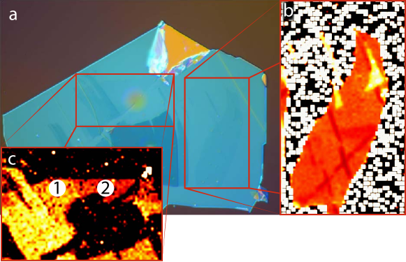
We confirm the presence or absence of a commensurate phase at the interface between the crystals by Raman spectroscopy. This is because the commensurate phase for graphene on hBN is characterised by the appearance of a strain distribution when the crystals near to alignment Woods et al. (2014). The Raman spectrum of graphene is sensitive to slight changes in uniaxial/biaxial strain. In particular, the 2D-peak responds to the commensurate phases’ strain distribution by broadening Eckmann et al. (2013). Here, we observe that the full-width half-maximum of the 2D-peak (FWHM(2D)) before our experiments is 23 cm-1, which is consistent with an unaligned flake ( misalignment) Eckmann et al. (2013), or graphene on a rough substrate (SiO2, polymers etc.) Ferrari and Basko (2013). This indicates that the graphene and hBN crystals cannot be in the commensurate phase.
After the phase transition, the FWHM(2D) shows significant change. The width of the peak has broadened to cm-1, which is consistent with the most aligned case of graphene on hBN ( alignment, moiré period is nm). Corresponding results are shown in Fig. 5. Here, insets b and c depict two single-layer graphene flakes. The moiré period obtained for the flake b is nm (FWHM(2D) is 33 cm-1). Moiré periods for areas (1) and (2) of the flake c are nm (FWHM(2D) is 40 cm-1) and nm (FWHM(2D) is 33 cm-1), respectively. This result demonstrates unambiguously that the graphene is now in a commensurate phase with the hBN crystal.
Encapsulated graphene
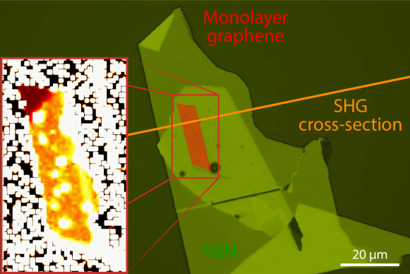
For additional confirmation of our findings, we repeat the nonlinear optical study on another sample. The optical picture of the sample is shown in Fig. 6. Here, a red area highlights an aligned monolayer graphene encapsulated between two hBN layers depicted by a light green color. The alignment of the graphene is confirmed by Raman spectroscopy. The moiré period is found to be nm (FWHM(2D) is 37 cm-1).
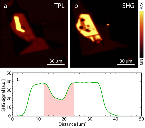
The TPL and SHG intensity pictures are shown in Fig. 7 a and b, respectively. Here, both, the TPL and SHG responses clearly shows the presence of a graphene flake. The change of the SHG signal from graphene with respect to the hBN environment confirms that the monolayer graphene flake is in the commensurate phase. The strong suppression of the SHG can be explicitly seen in Fig. 7 c that shows the cross-section of the SHG signal depicted by the orange line in Fig. 6. Here, the light red area corresponds to the position of the aligned single-layer graphene flake.