First-principles study of two-dimensional electron and hole gases at the head-to-head and tail-to-tail 180∘ domain walls in PbTiO3 ferroelectric thin films
Abstract
We study from first-principles the structural and electronic properties of head-to-head (HH) and tail-to-tail (TT) 180∘ domain walls in isolated free-standing PbTiO3 slabs. For sufficiently thick domains ( = 16 unit cells of PbTiO3), a transfer of charge from the free surfaces to the domain walls to form localized electron (in the HH) and hole (in the TT) gases in order to screen the bound polarization charges is observed. The electrostatic driving force behind this electronic reconstruction is clearly visible from the perfect match between the smoothed free charge densities and the bound charge distribution, computed from a finite difference of the polarization profile obtained after the relaxation of the lattice degrees of freedom. The domain wall widths, of around six unit cells, are larger than in the conventional 180∘ neutral configurations. Since no oxygen vacancies, defects or dopant atoms are introduced in our simulations, all the previous physical quantities are the intrinsic limits of the system. Our results support the existence of an extra source of charge at the domains walls to explain the enhancement of the conductivity observed in some domains walls of prototypical, insulating in bulk, perovskite oxides.
I INTRODUCTION
Domain walls (DWs) in oxide ferroelectric materials, defined as nanometer-scale interfaces that separate regions with different orientations of the spontaneous electric polarization, have attracted a lot of attention during the last few years due to the novel functional properties they might display, radically departing from those observed in the parent materials Catalan et al. (2012). One of these surprises comes from the observation of a room-temperature electronic conductivity at ferroelectric DWs in a thin-film insulating multiferroic BiFeO3 Seidel et al. (2009). Following this work, Guyonnet and co-workers Guyonnet et al. (2011) demostrated that 180∘ DWs in much simpler, purely ferroelectric tetragonal perovskite Pb(Zr0.2Ti0.8)O3 thin films were also conducting, suggesting that this phenomenon is more general than initially envisaged. Indeed, the presence of a conductive domain wall is not restricted to thin films, but equally applies to millimeter‐thick wide‐bandgap single crystals, such as LiNbO3 Schröder et al. (2012) or WO3 Kim et al. (2010). The microscopic origin of the conduction is controversial. It was first ascribed to structural changes at the DW that produced a polarization discontinuity, leading to steps in the electrostatic potential, and a concomitant lowering of the band gaps Seidel et al. (2009). More recently, it has been suggested that the conductivity could be linked with extrinsic factors, such as oxygen vacancies Farokhipoor and Noheda (2011); Guyonnet et al. (2011).
But other sources for a metallic type-conductivity at DWs have been proposed Bednyakov et al. (2018). Sluka et al. Sluka et al. (2013); Bednyakov et al. (2015) observed an enhancement of conductivity up to 109 times that of the parent matrix in charged DWs of the prototypical ferroelectric BaTiO3. This was attributed to the presence of a stable degenerate electron gas that would be formed to screen polarization divergences in head-to-head (HH) and tail-to-tail (TT) DWs Gureev et al. (2011). In conventional 180∘ domains in tetragonal ferroelectrics, the walls run parallel to the tetragonal polarization axis Pöykkö and Chadi (1999); Meyer and Vanderbilt (2002). In such a configuration, the polarization charge (defined as the dot product of the polarization times the unitary vector normal to the DW) vanishes, yielding to a neutral configuration. However, tilting of the DWs would lead to polarization-induced bound charges that would result in a large and unfavorable electrostatic energy Zhang et al. (2020). The extreme case, where the polarization points in the same direction as the normal vector to the wall, leads to the formation of head-to-head DWs (if the polarization is directed towards the DW; positive bound charges), or tail-to-tail DWs (if the polarization is directed outwards from the DW; negative bound charges). The properties of charged DWs might be very different from those of the neutral configurations. Different mechanisms have already been postulated in the literature to explain the screening of the polarization bound charges and stabilization of HH and TT 180∘ DWs in ferroelectrics. The theoretical background for the formation of charged domain walls in proper ferroelectrics based on a phenomenological model was established in Ref. Bednyakov et al., 2015, where an analysis of the different factors controlling the energy and the size of charged DWs was carried out. A mixed electron/ion screening scenario, with a combination of free equilibrium carriers coming from an electronic reconstruction (transfer of charge between the top of the valence band and the bottom of the conduction band due to a Zener-like breakdown) and a redistribution of the ionised impurities during the formation of the walls, seems the most favorable scenario. Phase field simulations support the existence of a degenerate quasi-two-dimensional electron gas, localized due to the potential well formed by the polarization charges Sluka et al. (2013). The application of a Landau model to address the problem of charged DWs in an isolated ferroelectric, including the polarization profile, width and formation energy of the domains was undertaken in Ref. Gureev et al., 2011. From a first-principles perspective, Wu and Vanderbilt Wu and Vanderbilt (2006) proposed a periodically repeated chemical “delta” doping in PbTiO3 superlattices, where the Ti atoms at certain layers are replaced by donor (Nb) or acceptor (Sc) atoms drawn from neighboring columns of the Periodic Table. Rahmanizadeh et al. Rahmanizadeh et al. (2014) suggested for the same material (i) the formation of a conducting layer at the domain wall in a superlattice geometry; (ii) the appearance of polarons due to the localization of one electron on a Ti ion (requiring for this the addition of an on-site Coulomb repulsion term) also in a superlattice geometry; and (iii) the presence of defects with various amounts of concentrations in thin film geometries. But in all the former first-principles simulations, the presence of substitutional atoms at one or the two HH and TT domain walls in the superlattices, or a varying defect concentration at the tails in the thin film geometry were assumed, and this fully determines the electric displacement, and therefore the polarization, within the domain as was shown in Ref. Stengel, 2011. Questions like what is the intrinsic critical thickness for the stabilization of the two-dimensional conducting layers for the screening of the polarization charges, the spatial extension of the hole and electron gases, or how large the polarization would be, if the HH and TT domain walls are induced in an ideal slab are not accessible from the previous computations. Similar issues regarding the screening of polarization discontinuities with electronic reconstructions have been the subject of intense studies in the celebrated LaAlO3/SrTiO3 interfaces (Ref. Stengel, 2011 and references therein), and theoretically in KNbO3/ATiO3 (A=Sr,Ba,Pb) superlattices Niranjan et al. (2009); García-Fernández et al. (2013). They have been also faced by Aguado-Puente et al. Aguado-Puente et al. (2015); Yin et al. (2015a) in a similar system to ours: an interface between a ferroelectric material like PbTiO3 and a dielectric like SrTiO3. Above a critical thickness of 16 unit cells, the ferroelectric layers could be stabilized in the out-of-plane monodomain configuration due to the electrostatic screening provided by the free carriers. We wonder whether the same results hold when the dielectric is replaced by an opposite domain, doubling the amount of polarization charge at the DW.
The rest of the paper is organized as follows: In Sec. II we describe the method on which the simulations are based. In Sec. III we present the results on the polarization profiles (Sec. III.1), the electronic properties including the layer-by-layer projected density of states (Sec. III.2), and the transfer of charge that yields to the formation of the two-dimensional hole and electron gases (Sec. III.3), together with the coupling between the electronic properties (density of free charge) and the structural properties (divergence of the polarization). Future perspectives are summarized in Sec. IV.
II Methods
We carried out simulations of HH and TT domain walls in a free standing slab of PbTiO3, within a numerical atomic orbital method as implemented in the Siesta code Soler et al. (2002). Exchange and correlation were treated within the local density approximation (LDA) Ceperley and Alder (1980) to the density functional theory (DFT) Hohenberg and Kohn (1964); Kohn and Sham (1965). While the use of an on-site Hubbard term for Ti would allow for a more realistic estimation of the band gap, we decided against taking this approach. The reason is that such a term would reduce the Ti -O hybridization, at the origin of the ferroelectric behaviour of PbTiO3 and, therefore, also behind the appearance of conductive domains in our simulations. In our tests in bulk PbTiO3 we could not find a U that reproduced the band gap and gave, at the same time, a reasonable value for the material’s polarization (indeed, the total polarization falls dramatically for values of U 2 eV, and vanishes for a U 3 eV). Nevertheless, we have to keep in mind that within the bare LDA approach, the band gap is severely understimated, with a concomitant reduction of the critical thickness for the stabilization of the conducting layers (in simple models it is proportional to the band gap width).
Core electrons were replaced by ab initio norm conserving pseudopotentials, generated using the Troullier-Martins scheme Troullier and Martins (1991) in the Kleinman-Bylander fully non-local separable representation Kleinman and Bylander (1982). Due to the large overlap between the semicore and valence states, the semicore and electrons of Ti, and the electrons of Pb were considered as valence electrons and explicitly included in the simulations. Ti and Pb pseudopotentials were generated scalar relativistically. The reference configuration and cutoff radii for each angular momentum shell for the pseudopotentials used in this work can be found in Ref. Junquera et al., 2003 for Ti and O, and in Table 1 for Pb.
| Reference | ||
|---|---|---|
| Core radius | 2.00 | |
| 2.30 | ||
| 2.00 | ||
| 1.50 | ||
| Scalar relativistic? | yes |
The one-electron Kohn-Sham eigenstates were expanded in a basis of strictly localized numerical atomic orbitals Sankey and Niklewski (1989); Artacho et al. (1999). We used a single- basis set for the semicore states of Ti and Pb, and double- plus polarization for the valence states of all the atoms. For Pb, an extra shell of 5 orbitals was added. All the parameters that define the shape and range of the basis functions were obtained by a variational optimization of the energy Junquera et al. (2001) in bulk cubic BaTiO3 (for Ti, and O). For Pb, another optimization was performed in bulk PbTiO3, frozen in the atomic orbitals of Ti and O to those previously optimized in BaTiO3 bas .
The electronic density, Hartree, and exchange-correlation potentials, as well as the corresponding matrix elements between orbitals, were calculated in a uniform real-space grid, with an equivalent plane-wave cutoff of 1200 Ry in the representation of charge density. For the Brillouin zone integrations we use a Monkhorst-Pack sampling Monkhorst and Pack (1976) equivalent to in a five atom perovskite unit cell. A Fermi-Dirac distribution was chosen for the occupation of the one-particle Kohn-Sham electronic eigenstates, with a smearing temperature of 250 K for the HH and 500 K for the TT domain structures.
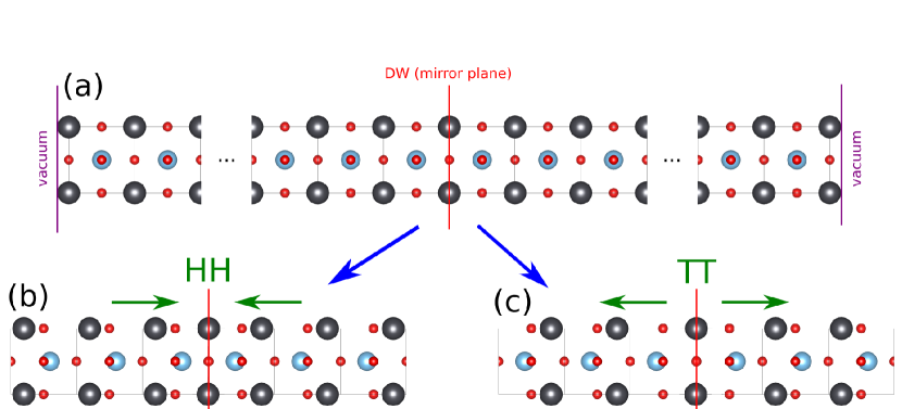
To simulate both domain structures we used a tetragonal supercell, periodically repeated in space, of the type vacuum/(PbO-TiO2)2n-PbO/vacuum with , as shown in Fig. 1 (simulations with =12 showed that the system went back to the paraelectric structure without stabilizing the metallic gases). Both surfaces were terminated with a PbO layer, since this is the only stable surface termination found by first-principles Meyer et al. (1999). The vacuum thickness was equivalent to roughly eight unit cells of the perovskite. A dipole correction was introduced to avoid spurious interaction between periodic images of the slab in the out-of-plane direction. In this way, we also enforce that the electric displacement field in vacuum vanishes, and due to the continuity of its normal component at the free-surface, after the electronic reconstruction it exactly amounts within the PbTiO3 domain to the surface charge density. In order to simulate the effect of the mechanical boundary conditions due to the strain imposed by an hypothetical substrate, the in-plane lattice constant was fixed to the theoretical equilibrium lattice constant of bulk SrTiO3 ( Å), one of the most common substrates used to grow oxide heterostructures. In constrained bulk PbTiO3 under this compressive strain, the spontaneous polarization amounts to C/cm2. As the initial point, an ideal structure was defined stacking along the [001] direction unit cells of PbTiO3 in a tetragonal paraelectric configuration (i. e. zero rampling in all the atomic layers) with a tetragonality of . Then, on top of this paraelectric structure, the PbTiO3 atoms were moved in opposite directions in the two halves of the slab geometry following the displacement pattern of the bulk tetragonal soft mode scaled to 62%. That is the value of the polarization of a meta-stable structure of a monodomain PbTiO3 slab where the polarization charge can be screened by an electronic reconstruction and the formation of two-dimensional metallic gases at the surfaces Aguado-Puente et al. (2015). By construction, the central PbO layer is a mirror symmetry plane. As it was discussed in Ref. Meyer and Vanderbilt, 2002 there is no indication from first-principles simulations that the energy of the Pb-centered domain wall can be lowered by breaking the inversion symmetry. Starting from this geometry, a conjugate gradient minimization was performed till the maximum component of the force on any atom was smaller than 0.04 eV/Å.
Once the atomic structure is relaxed and the one-particle density matrix converged, in order to compute the density of states, a non-self-consistent calculation was carried out with a much denser sampling of Monkhorst-Pack mesh.
To establish the notation, we shall call the plane parallel to the interface the plane, whereas the perpendicular direction will be referred to as the axis.
III Results
III.1 Polarization profiles
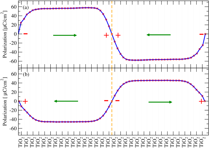
After relaxation of the slabs with unit cells in each domain, we observe how the two polar configurations are meta-stable, while the most stable phase is the centrosymmetric unpolarized structure. A similar result was found in the PbTiO3/SrTiO3 interfaces Yin et al. (2015a). The TT configuration is more stable than the HH, as can be seen from the differences in energy with respect the centrosymmetric paraelectric phase shown in Table 2.
In Fig. 2 we plot the layer-by-layer effective polarization profile in the HH [Fig. 2(a)] and TT [Fig. 2(b)] domain structures for PbTiO3. The layer polarizations have been calculated using the approximate expression based on the effective Born charge method, where the bulk dynamical charges have been re-normalized, following the recipe given in Ref. Stengel et al., 2011. The polarization profile is remarkably flat within the interior of the domains, characterized by a constant value that amounts to 57.26 C/cm2 (0.74 ) and 45.72 C/cm2 (0.59 ) for the HH and TT structures, respectively. At the domain walls and at the free surfaces we observe a spatial variation of , result of localized strong non-homogeneous atomic distortions. The extension of these regions with non-uniform polarizations, of approximately six unit cells, allow us to quantify the width of the domain walls. A more qualitative information can be extracted from a fit of the polarization profile to the functional form derived by Gureev et al. Gureev et al. (2011),
| (1) |
where is the typical half-width of the domain wall (i.e. to make the transition from to we need a space of four times this length . The results of the fitting of the profiles shown in Fig. 2 to the model summarized in Eq. (1) can be found in Table 2.
| (C/cm2) | (Å) | (eV) | |
|---|---|---|---|
| HH | 57.26 | 5.80 | 1.374 |
| TT | 45.72 | 6.87 | 1.160 |
Clearly, the domain wall widths are larger than in the neutral configuration, where they were found to be very narrow, of the order of the lattice constant Meyer and Vanderbilt (2002), also supporting the conclusions of Ref. Gureev et al., 2011.
These 180∘ domain walls, where the wall is perpendicular to the polarization, give rise to polarization-induced bound charges, that lead to the local concentration of a large electrostatic energy that destabilizes this configuration. The stabilization of the domains observed in Fig. 2 implies that the positive (for the HH) and negative (for the TT) polarization charges at the domain wall have been screened. Since in our calculations we do not consider the presence of defects or dopants Wu and Vanderbilt (2006), the most plausible scenario is the metallization of the domain wall and the free surfaces due to the neutralization by free carriers, yielding to the formation of thin quasi-two-dimensional metallic layers. The fingerprint to characterize such scenario would be the presence of a substantial amount of free charge populating the band edges (top of the valence band and bottom of the conduction band) both at the domain wall and at the free surfaces of the slab.
III.2 Layer by layer PDOS
Fig. 3 shows the layer (spatially) resolved PDOS on all the atomic orbitals of the Ti and O atoms at the TiO2 layers of the different PbTiO3 unit cells. The bottom layer plotted in Fig. 3 is adjacent to the free surface and the top one lies close to the domain wall. Only the PDOS for one of the domains are shown, since there is a mirror symmetry plane at the domain wall. (As shown in Ref. Stengel, 2011 the equilibrium distribution and spreading of the electron gas is uniquely determined by the boundary values of the electric displacement field, that can be indeed set in an asymmetric way. Those asymmetric configurations are beyond the scope of the present work). All the PDOS curves were calculated following the recipe given in Sec. III.A.1 of Ref. Stengel et al., 2011 with the Dirac delta functions for the eigenvalues in the PDOS computations replaced by smearing normalized Gaussians with a finite width that is twice as large, as suggested in Appendix B of Ref. Stengel et al., 2011. On top of the heterostructure PDOS we superimpose the bulk PDOS (dashed red lines), calculated with an equivalent -point sampling. The bulk reference calculation was computed from a periodic bulk calculation with a five atom per unit cell PbTiO3 structure, with the atomic distortions and out-of-plane strain extracted from a region of the HH or TT domains where the relaxed atomic structure (Fig. 2) has converged into a regular pattern. Then we extract the PDOS for the same TiO2 atomic layer. Finally,we note that the superposition of the bulk PDOS and supercell PDOS at each layer was done by matching the sharp peaks of the Ti(3) semicore band.
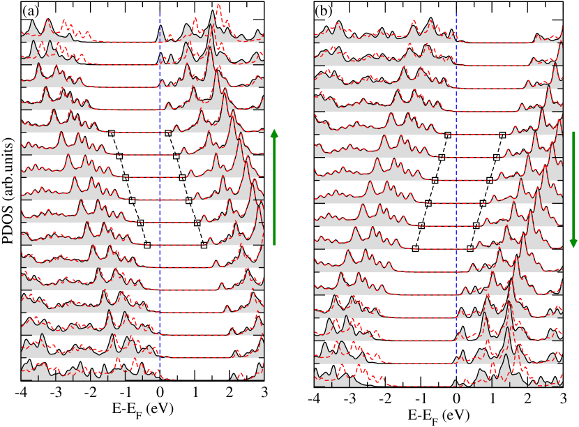
First of all, it is remarkable to check how for the perovskite material studied in this work, PbTiO3, and even upon the electronic reconstruction and metallization, a well-defined energy gap persists in all layers between the bands that are mostly O- in character (top of the valence band at the bulk level), and the bands that are mostly Ti- in character (bottom of the conduction band at the bulk level).
The local metallization of the free-surface layers and the domain wall is evident from the location of the valence-band top and the conduction-band bottom of these layers with respect to the Fermi level of the whole structure, taken as zero in Fig. 3. For the HH domain configuration [Fig. 3(a)], the non-vanishing PDOS at the Fermi level for the three topmost TiO2 layers points to the electronic population of the conduction-band bottom of the PbTiO3 unit cells close to the domain wall. This free electronic charge has been transferred from the free surface, as can be clearly seen from the generation of holes at the bottom-most layers (see the crossing of the Fermi level with the PDOS at the valence-band top for the three bottom-most TiO2 layers). For the TT domain configuration [Fig. 3(b)], the same behaviour is found, but with the role of the electrons and holes interchanged (i.e. generation of holes at the top of the valence band in the layers adjacent to the domain wall, and the population of the bottom of the conduction band with electrons close to the free surfaces).
The PDOS of the conduction and valence bands converges fairly quickly to the bulk curve when moving away from the interface, and the PDOS vanish at the Fermi level, which implies that the system is locally insulating. Furthermore, the PDOS in each layer appears rigidly shifted with respect to the neighboring two layers, consistent with the presence of an internal remnant depolarization field that keep the free charges electrostatically confined to the metallic region within the domains Stengel et al. (2011) (see black dashed lines in Fig. 3). Since the bulk calculations were performed at zero external electric field, while in the slab calculations there is a residual depolarizing field, the coincidence of the two curves far enough from the free surfaces and the domain wall means that the main effect on the layer by layer PDOS comes from the lattice distortions, and not from macroscopic depolarizing fields. This residual depolarizing field will play a major role in the determination of the atomic orbitals involved in the electronic reconstruction, as will be discussed below.
III.3 Coupling between density of free carriers and the polarization profiles
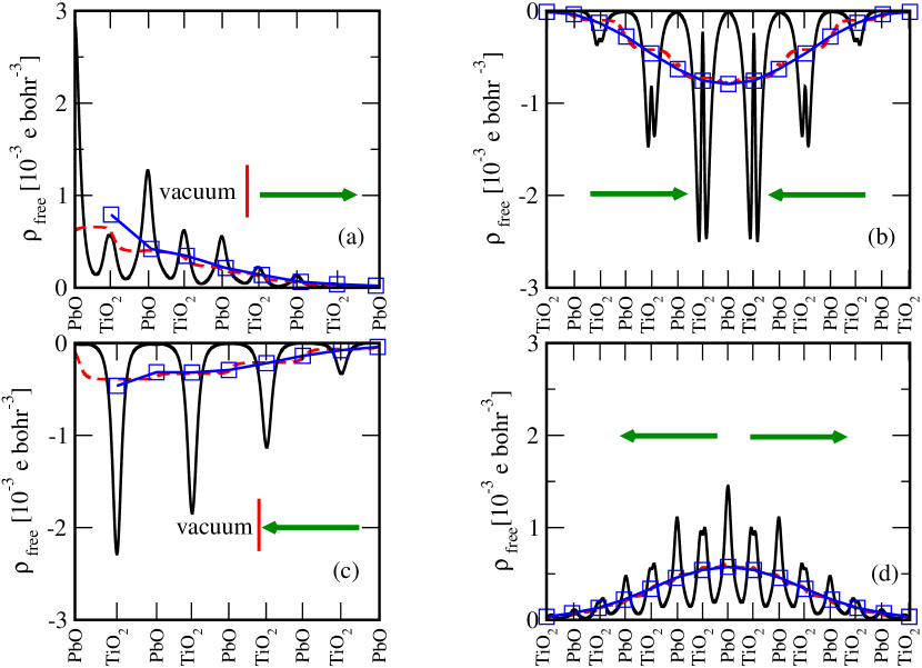
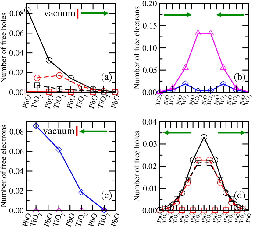
To estimate the amount of charge that has been transferred from the free-surfaces to the domain wall in order to screen the depolarizing fields, we plot in Fig. 4 the planar average of the free charge, , defined as
| (2) |
where is the area of the interface unit cell, and the corresponding nanosmoothed version Junquera et al. (2007), . For the electronic charge density populating the bottom of the conduction band has been computed as
| (3) |
while for the hole charge density populating the top of the valence band, it amounts to
| (4) |
where is the weight of a special point in the discrete Monkhorst-Pack mesh, are the occupation numbers of the eigenstate and the sum is restricted to the states with eigenvalue higher than , a value of the energy corresponding to the center of the gap between valence and conduction band. The results are shown in Fig. 4.
Again, we clearly see that the system is not locally charge neutral at the domain wall and at the free-surfaces. If the profiles of the nanosmoothed average free charge densities are integrated along , we can extract the free-carrier per unit area, labeled as (for the electrons) and (for the holes). For the HH domains, there is an additional electron density at the domain wall populating the bottom of the conduction bands that amounts to = 1.033 electrons [Fig. 4(a)]. Those electrons are transferred from the free-surfaces, where the integration of the free hole charge in Fig. 4(b) yields a value of = 0.517 holes per surface unit cell. As required by the global charge neutrality (we have two free surfaces populated with holes and just one HH domain wall charged with electrons).
For the TT domains, the extra holes at the domain wall [Fig. 4(c)] equals = 0.827, that again just double the number of extra electrons populating the bottom of the conduction bands at the free-surfaces, = 0.413 [Fig. 4(d)].
A further insight on the origin of these electron and hole free charges can be drawn after its decomposition into different orbital components, as it is done in Fig. 5. The current wisdom is that the orbitals are the first to be populated in the related LaAlO3/SrTiO3 Popović et al. (2008) or PbTiO3/SrTiO3 Yin et al. (2015a) interfaces, where two-dimensional electron gases are formed to screen the polar catastrophe. This situation is similar to that found in bulk polarized PbTiO3 and also observed in the free surface of our system [Fig. 5(c)]. However, when discussing the metallic states formed around the domain walls we can observe, on the one hand, that the HH electron gas (Fig. 5b) is, for the most part, formed by and orbitals, while ones host very little charge. This can also be observed in the doubled-peaks of Fig. 4b. On the other hand, the TT hole gas has a primary contribution from the -orbitals in the PbO plane (i.e. and orbitals in the oxygen at the PbO layer) and a smaller, but also significant, contribution from both (i.e. the , respectively , orbital of the equatorial O located along , respectively , with respect the Ti) and -bonded orbitals (i.e. the and , respectively and , orbitals of the equatorial O located along , respectively , with respect the Ti) in TiO2 planes. Both facts are consistent with the effects of localization due to the remnant electric potential energy within the domains, whose shape resembles a for the HH and for the TT, with the peak located right at the domain wall in both cases. Those are confinement potentials for the respective carriers. For the bands with majority weights on orbitals directed parallel to the domain wall, there is no effect on the dispersion; only the center of the subbands might be displaced following exactly the shape of the potential. This is the case of the bands of Ti, and on the O- orbitals. However, the bands with majority weights on orbitals directed perpendicular to the domain wall, both the dispersion and the local center of mass of the bands are strongly modified due to the confinement potential: the range of the possible interactions is strongly reduced. As a consequence the hybridization is decreased, and the corresponding bonding orbitals (O- orbitals in PbO layers) increase the energy and the antibonding orbitals (,) suffer a concomitant reduction. Those are the first orbitals to be filled with electrons [Fig. 5(b)] or emptied to create holes [Fig. 5(d)] around the domain wall.
In order to elucidate how this electronic reconstruction is a result of the screening of the polarization-induced charges at the 180∘ domain walls, we also plot in Fig. 4 a numerical differentiation of the polarization profile shown in Fig. 2. There is an essentially perfect matching between the nanosmoothed free charge densities and the bound charge profile, (blue lines in Fig. 4), defined as . Therefore, the polarization discontinuity at the domain wall is the driving force for the electronic reconstruction, and this transfer of charge between the domain wall and the free surface provides an effective screening mechanism that stabilizes the monodomain configurations in both domains.
IV Conclusions
Our density-functional simulations have shown how 180∘ HH and TT charged domains can be stabilized in the out-of-plane monodomain configuration in an ideal PbTiO3 slab (no dopants nor vacancies), thanks to the electrostatic screening provided by free carriers. Above a critical size of the domains, in our case = 16 unit cells, an electronic reconstruction takes place, where charge is transferred from the free-surface of the slab to the domain wall, and generates quasi-two-dimensional electron and hole gases. The width of the domain wall of around 6 (for the HH) and 7 (for the TT) unit cells, is much larger than the typical width of neutral domains (of the order of one lattice constant). A clear electrostatic coupling between the density of free-charge and the polarization profile, whose negative gradient equals the bound charge, is found.
Our results support previous phenomenological models based on Landau and semiconductor theory, regarding the existence of quasi-two-dimensional charge densities at the 180∘ HH-TT domain walls in isolated ferroelectric Gureev et al. (2011), and postulated them to be the driving force for the metallic like conductivity found at the walls between insulating polar materials Sluka et al. (2013).
The driving force for the accumulation of free charges at the domain wall is the mismatch of the formal polarization between the constituent materials Aguado-Puente et al. (2015); Yin et al. (2015b). (This formal polarization corresponds to the raw result of a Berry phase calculation Stengel and Vanderbilt (2009).) Therefore, in the quest of searching for potential domain walls where this scenario can occur, the larger the polarization mismatch, the better. In a ferroelectric material, the formal polarization can be tuned with electric fields, strain, or temperature, offering more degrees of freedom than the celebrated two-dimensional electron gas at the SrTiO3/LaAlO3 interface Ohtomo and Hwang (2004), where the formal polarization in LaAlO3 is due to the fact that the individual LaO and AlO2 layers have formal charges of Stengel and Vanderbilt (2009). Also, it is important to note that the smaller the band gap of the material, the shorter the critical thickness required by the electrostatic potential to close the gap, and the sooner the charged domain walls would appear.
These first-principles simulations might serve as benchmarks to perform second-principles computations that include all the relevant electronic and lattice degrees of freedom García-Fernández et al. (2016) in very large systems under operating conditions of field and temperature. Once the atomistic and electronic models for the second-principles calculations will be validated, then more challenging calculations including tilting domains like the ones that appear during domain switching, or the conductivity at domain walls can be tackled.
ACKNOWLEDGMENT
We acknowledge Pablo Aguado-Puente for the useful discussions we had during the course of this work. J.S. thanks the University of Cantabria for the scholarship funded by the Vice-rectorate for Internationalisation and the Theoretical Condensed Matter Group. We gratefully acknowledge the African school for Electronic Structure Methods and Applications (ASESMA), especially Richard Martin, for assisting in bringing us together to form our collaboration. J.J. and P.G.-F. acknowledge financial support from the Spanish Ministry of Economy and Competitiveness through the MINECO Grant No. FIS2015-64886-394-C5-2-P, and the Spanish Ministry of Science, Innovation and Universities through the grant No. PGC2018-096955-B-C41. P.G.-F. acknowledges support from Ramón y Cajal Grant No. RyC-2013-12515. G.S.M acknowledges support from the Kenya Education Network through CMMS mini-grant 2019/2020. The authors also gratefully acknowledge the computer resources, technical expertise, and assistance provided by the Centre for High Performance Computing (CHPC), Cape Town, South Africa.
References
- Catalan et al. (2012) G. Catalan, J. Seidel, R. Ramesh, and J. F. Scott, Rev. Mod. Phys. 84, 119 (2012).
- Seidel et al. (2009) J. Seidel, L. W. Martin, Q. He, Q. Zhan, Y.-H. Chu, A. Rother, M. E. Hawkridge, P. Maksymovych, P. Yu, M. Gajek, N. Balke, S. V. Kalinin, S. Gemming, F. Wang, G. Catalan, J. F. Scott, N. A. Spaldin, J. Orenstein, and R. Ramesh, Nat. Mater. 8, 229 (2009).
- Guyonnet et al. (2011) J. Guyonnet, I. Gaponenko, S. Gariglio, and P. Paruch, Adv. Mater. 23, 5377 (2011).
- Schröder et al. (2012) M. Schröder, A. Haußmann, A. Thiessen, E. Soergel, T. Woike, and L. M. Eng, Adv. Funct. Mater. 22, 3936 (2012).
- Kim et al. (2010) Y. Kim, M. Alexe, and E. K. H. Salje, Appl. Phys. Lett. 96, 032904 (2010).
- Farokhipoor and Noheda (2011) S. Farokhipoor and B. Noheda, Phys. Rev. Lett. 107, 127601 (2011).
- Bednyakov et al. (2018) P. S. Bednyakov, B. I. Sturman, T. Sluka, A. K. Tagantsev, and P. V. Yudin, npj Computational Materials 4, 1 (2018).
- Sluka et al. (2013) T. Sluka, A. K. Tagantsev, P. Bednyakov, and N. Setter, Nat. Commun. 4, 1808 (2013).
- Bednyakov et al. (2015) P. S. Bednyakov, T. Sluka, A. K. Tagantsev, D. Damjanovic, and N. Setter, Sci. Rep. 5, 15819 (2015).
- Gureev et al. (2011) M. Y. Gureev, A. K. Tagantsev, and N. Setter, Phys. Rev. B 83, 184104 (2011).
- Pöykkö and Chadi (1999) S. Pöykkö and D. J. Chadi, Appl. Phys. Lett. 75, 2830 (1999).
- Meyer and Vanderbilt (2002) B. Meyer and D. Vanderbilt, Phys. Rev. B 65, 104111 (2002).
- Zhang et al. (2020) J. Zhang, Y.-J. Wang, J. Liu, J. Xu, D. Wang, L. Wang, X.-L. Ma, C.-L. Jia, and L. Bellaiche, Phys. Rev. B 101, 060103 (2020).
- Wu and Vanderbilt (2006) X. Wu and D. Vanderbilt, Phys. Rev. B 73, 020103 (2006).
- Rahmanizadeh et al. (2014) K. Rahmanizadeh, D. Wortmann, G. Bihlmayer, and S. Blügel, Phys. Rev. B 90, 115104 (2014).
- Stengel (2011) M. Stengel, Phys. Rev. Lett. 106, 136803 (2011).
- Niranjan et al. (2009) M. K. Niranjan, Y. Wang, S. S. Jaswal, and E. Y. Tsymbal, Phys. Rev. Lett. 103, 016804 (2009).
- García-Fernández et al. (2013) P. García-Fernández, P. Aguado-Puente, and J. Junquera, Phys. Rev. B 87, 085305 (2013).
- Aguado-Puente et al. (2015) P. Aguado-Puente, N. C. Bristowe, B. Yin, R. Shirasawa, P. Ghosez, P. B. Littlewood, and E. Artacho, Phys. Rev. B 92, 035438 (2015).
- Yin et al. (2015a) B. Yin, P. Aguado-Puente, S. Qu, and E. Artacho, Phys. Rev. B 92, 115406 (2015a).
- Soler et al. (2002) J. M. Soler, E. Artacho, J. D. Gale, A. García, J. Junquera, P. Ordejón, and D. Sánchez-Portal, J. Phys.: Condens. Matter 14, 2745 (2002).
- Ceperley and Alder (1980) D. M. Ceperley and B. J. Alder, Phys. Rev. Lett. 45, 566 (1980).
- Hohenberg and Kohn (1964) P. Hohenberg and W. Kohn, Phys. Rev. 136, B864 (1964).
- Kohn and Sham (1965) W. Kohn and L. J. Sham, Phys. Rev. 140, A1133 (1965).
- Troullier and Martins (1991) N. Troullier and J. L. Martins, Phys. Rev. B 43, 1993 (1991).
- Kleinman and Bylander (1982) L. Kleinman and D. M. Bylander, Phys. Rev. Lett. 48, 1425 (1982).
- Junquera et al. (2003) J. Junquera, M. Zimmer, P. Ordejón, and P. Ghosez, Phys. Rev. B 67, 155327 (2003).
- Sankey and Niklewski (1989) O. F. Sankey and D. J. Niklewski, Phys. Rev. B 40, 3979 (1989).
- Artacho et al. (1999) E. Artacho, D. Sánchez-Portal, P. Ordejón, A. García, and J. M. Soler, Phys. Status Solidi (b) 215, 809 (1999).
- Junquera et al. (2001) J. Junquera, O. Paz, D. Sánchez-Portal, and E. Artacho, Phys. Rev. B 64, 235111 (2001).
- (31) Values for the parameters can be obtained upon request.
- Monkhorst and Pack (1976) H. J. Monkhorst and J. D. Pack, Phys. Rev. B 13, 5188 (1976).
- Meyer et al. (1999) B. Meyer, J. Padilla, and D. Vanderbilt, Faraday Discuss. 114, 395 (1999).
- Stengel et al. (2011) M. Stengel, P. Aguado-Puente, N. A. Spaldin, and J. Junquera, Phys. Rev. B 83, 235112 (2011).
- Junquera et al. (2007) J. Junquera, M. H. Cohen, and K. M. Rabe, J. Phys.: Condens. Matter 19, 213203 (2007).
- Popović et al. (2008) Z. S. Popović, S. Satpathy, and R. M. Martin, Phys. Rev. Lett. 101, 256801 (2008).
- Yin et al. (2015b) B. Yin, P. Aguado-Puente, S. Qu, and E. Artacho, Phys. Rev. B 92, 115406 (2015b).
- Stengel and Vanderbilt (2009) M. Stengel and D. Vanderbilt, Phys. Rev. B 80, 241103 (2009).
- Ohtomo and Hwang (2004) A. Ohtomo and H. Y. Hwang, Nature 427, 423 (2004).
- García-Fernández et al. (2016) P. García-Fernández, J. C. Wojdeł, J. Íñiguez, and J. Junquera, Phys. Rev. B 93, 195137 (2016).